TH72032
868/915MHz
ASK Transmitter
3901072032
Page 1 of 14
Data Sheet
Rev. 004
Feb./03
PR
ELI
MIN
AR
Y
Features
!
Fully integrated PLL-stabilized VCO
!
Frequency range from 850 MHz to 930 MHz
!
Single-ended
RF
output
!
ASK achieved by on/off keying of internal
power amplifier up to 40 kbit/s
!
Wide power supply range from 1.9 V to 5.5 V
!
Very low standby current
!
Low
voltage
detector
!
High over-all frequency accuracy
!
Adjustable output power range from
-12 dBm to +8.5 dBm
!
Adjustable current consumption from
4.0 mA to 14.0 mA
!
Conforms to EN 300 220 and similar standards
Ordering Information
Part No.
Temperature Code
Package Code
TH72032
K (-40 C° to 125 °C)
DC (SOIC8)
Application Examples
Pin Description
!
General digital data transmission
!
Tire Pressure Monitoring System (TPMS)
!
Remote Keyless Entry (RKE)
!
Low-power
telemetry
!
Alarm and security systems
!
Garage door openers
!
Home
automation
General Description
The TH72032 ASK transmitter IC is designed for applications in the European 868 MHz industrial-scientific-
medical (ISM) band, according to the EN 300 220 telecommunications standard. It can also be used for any
other system with carrier frequencies ranging from 850 MHz to 930 MHz (e.g. for applications in the US 915
MHz ISM band).
The transmitter's carrier frequency f
c
is determined by the frequency of the reference crystal f
ref
. The
integrated PLL synthesizer ensures that each RF value, ranging from 850 MHz to 930 MHz, can be achieved
by using a crystal with a reference frequency according to: f
ref
= f
c
/N, where N = 32 is the PLL feedback
divider ratio.
n. c.
ASKDTA
VEE
ENTX
ROI
VCC
PSEL
OUT
TH72032
1
3
4
2
8
6
5
7

TH72032
868/915MHz
ASK Transmitter
3901072032
Page 2 of 14
Data Sheet
Rev. 004
Feb./03
PR
ELI
MIN
AR
Y
Document Content
1
Theory of Operation...................................................................................................3
1.1 General .............................................................................................................................. 3
1.2 Block Diagram.................................................................................................................... 3
2
Functional Description ..............................................................................................4
2.1 Crystal Oscillator................................................................................................................ 4
2.2 ASK Modulation ................................................................................................................. 4
2.3 Crystal Pulling .................................................................................................................... 4
2.4 Output Power Selection ..................................................................................................... 5
2.5 Lock Detection ................................................................................................................... 5
2.6 Low Voltage Detection ....................................................................................................... 5
2.7 Mode Control Logic ............................................................................................................ 6
2.8 Timing Diagrams................................................................................................................ 6
3
Pin Definition and Description ..................................................................................7
4
Electrical Characteristics ..........................................................................................8
4.1 Absolute Maximum Ratings................................................................................................ 8
4.2 Normal Operating Conditions ............................................................................................. 8
4.3 Crystal Parameter .............................................................................................................. 8
4.4 DC Characteristics ............................................................................................................. 9
4.5 AC Characteristics ........................................................................................................... 10
4.6 Output Power Steps ......................................................................................................... 10
5
Test Circuit ...............................................................................................................11
5.1 Test circuit component list to Fig. 5 .................................................................................. 11
6
Package Information................................................................................................12
7
Reliability Information..............................................................................................13
8
ESD Precautions ......................................................................................................13
9
Disclaimer .................................................................................................................14
TH72032
868/915MHz
ASK Transmitter
3901072032
Page 3 of 14
Data Sheet
Rev. 004
Feb./03
PR
ELI
MIN
AR
Y
1
Theory of Operation
1.1 General
As depicted in Fig.1, the TH72032 transmitter consists of a fully integrated voltage-controlled oscillator
(VCO), a divide-by-32 divider (div32), a phase-frequency detector (PFD) and a charge pump (CP). An
internal loop filter determines the dynamic behavior of the PLL and suppresses reference spurious signals. A
Colpitts crystal oscillator (XOSC) is used as the reference oscillator of a phase-locked loop (PLL)
synthesizer. The VCO's output signal feeds the power amplifier (PA). The RF signal power P
out
can be
adjusted in four steps from P
out
= 12 dBm to +8.5 dBm, either by changing the value of resistor RPS
or by
varying the voltage V
PS
at pin PSEL. The open-collector output (OUT) can be used either to directly drive a
loop antenna or to be matched to a 50Ohm load. Bandgap biasing ensures stable operation of the IC at a
power supply range of 1.9 V to 5.5 V.
1.2 Block
Diagram
Fig. 1: Block diagram with external components
VEE
XOSC
PA
XBUF
VCO
PLL
CP
PFD
32
PSEL
RPS
ROI
XTAL
8
5
3
2
antenna
matching
network
OUT
7
CX1
1
ASKDTA
6
VCC
mode
control
ENTX
4
low
voltage
detector

TH72032
868/915MHz
ASK Transmitter
3901072032
Page 4 of 14
Data Sheet
Rev. 004
Feb./03
PR
ELI
MIN
AR
Y
2
Functional Description
2.1 Crystal
Oscillator
A Colpitts crystal oscillator with integrated functional capacitors is used as the reference oscillator for the PLL
synthesizer. The equivalent input capacitance CRO offered by the crystal oscillator input pin ROI is about
18pF. The crystal oscillator is provided with an amplitude control loop in order to have a very stable
frequency over the specified supply voltage and temperature range in combination with a short start-up time.
2.2 ASK
Modulation
The PLL transmitter can be ASK-modulated by
applying a data stream directly at the pin
ASKDTA. This turns the internal current
sources of the power amplifier on and off and
therefore leads to an ASK signal at the output.
ASKDTA
Description
0
Power amplifier is turned off
1
Power amplifier is turned on (according
to the selected output power step)
2.3 Crystal
Pulling
A crystal is tuned by the manufacturer to the
required oscillation frequency f
0
at a given load
capacitance CL and within the specified
calibration tolerance. The only way to pull the
oscillation frequency is to vary the effective load
capacitance CL
eff
seen by the crystal.
Figure 2 shows the oscillation frequency of a
crystal as a function of the effective load
capacitance. This figure also illustrates the
relationship between the external pulling
capacitor and the center frequency.
It can be seen that the pulling sensitivity
increases with the reduction of CL. For high-
accuracy ASK applications, a higher load
capacitance should be chosen in order to
reduce the frequency drift caused by the
tolerances of the chip and the external pulling
capacitor.
Fig. 2: Crystal pulling characteristic
f
o
f
eff
CL
eff
CL
R1
C1
C0
L1
XTAL
CL=
CX1 CRO
CX1+CRO

TH72032
868/915MHz
ASK Transmitter
3901072032
Page 5 of 14
Data Sheet
Rev. 004
Feb./03
PR
ELI
MIN
AR
Y
2.4 Output Power Selection
The transmitter is provided with an output power selection feature. There are four predefined output power
steps and one off-step accessible via the power selection pin PSEL. A digital power step adjustment was
chosen because of its high accuracy and stability. The number of steps and the step sizes as well as the
corresponding power levels are selected to cover a wide spectrum of different applications.
The implementation of the output power control
logic is shown in figure 3. There are two
matched current sources with an amount of
about 8 µA. One current source is directly
applied to the PSEL pin. The other current
source is used for the generation of reference
voltages with a resistor ladder. These reference
voltages are defining the thresholds between
the power steps. The four comparators deliver
thermometer-coded control signals depending
on the voltage level at the pin PSEL. In order to
have a certain amount of ripple tolerance in a
noisy environment the comparators are
provided with a little hysteresis of about 20 mV.
With these control signals, weighted current
sources of the power amplifier are switched on
or off to set the desired output power level
(Digitally Controlled Current Source). The
LOCK, ASK signal and the output of the low
voltage detector are gating this current source.
Fig. 3: Block diagram of output power control circuitry
There are two ways to select the desired output power step. First by applying a DC voltage at the pin PSEL,
then this voltage directly selects the desired output power step. This kind of power selection can be used if
the transmission power must be changed during operation. For a fixed-power application a resistor can be
used which is connected from the PSEL pin to ground. The voltage drop across this resistor selects the
desired output power level. For fixed-power applications at the highest power step this resistor can be
omitted. The pin PSEL is in a high impedance state during the "TX standby" mode.
2.5 Lock
Detection
The lock detection circuitry turns on the power amplifier only after PLL lock. This prevents from unwanted
emission of the transmitter if the PLL is unlocked.
2.6 Low Voltage Detection
The supply voltage is sensed by a low voltage detect circuitry. The power amplifier is turned off if the supply
voltage drops below a value of about 1.85 V. This is done in order to prevent unwanted emission of the
transmitter if the supply voltage is too low.
ASKDTA
&
&
&
PSEL
&
&
RPS
OUT

TH72032
868/915MHz
ASK Transmitter
3901072032
Page 6 of 14
Data Sheet
Rev. 004
Feb./03
PR
ELI
MIN
AR
Y
2.7 Mode Control Logic
The mode control logic allows two different
modes of operation as listed in the following
table. The mode control pin ENTX is pulled-
down internally. This guarantees that the whole
circuit is shut down if this pin is left floating.
ENTX
Mode
Description
0
TX standby
TX disabled
1
TX active
TX enable
2.8 Timing
Diagrams
After enabling the transmitter by the ENTX signal, the power amplifier remains inactive for the time t
on
, the
transmitter start-up time. The crystal oscillator starts oscillation and the PLL locks to the desired output
frequency within the time duration t
on
. After successful PLL lock, the LOCK signal turns on the power
amplifier, and then the RF carrier can be ASK modulated.
Fig. 4: Timing diagram for ASK modulation
low
low
high
high
LOCK
ASKDTA
RF carrier
t
low
high
ENTX
t
on

TH72032
868/915MHz
ASK Transmitter
3901072032
Page 7 of 14
Data Sheet
Rev. 004
Feb./03
PR
ELI
MIN
AR
Y
3
Pin Definition and Description
Pin No.
Name
I/O Type
Functional Schematic
Description
1
ASKDTA
input
1.5k
1
0: ENTX=1
1: ENTX=0
ASKDTA
ASK data input,
CMOS compatible with
operation mode dependent
pull-up circuit
TX standby: no pull-up
TX active: pull-up
2
n. c.
no connection
3
ROI
analog I/O
ROI
3
36p
36p
25k
XOSC connection to XTAL,
Colpitts type crystal
oscillator
4
ENTX
input
ENTX
4
1.5k
mode control input,
CMOS-compatible with
internal pull-down circuit
5
PSEL
analog I/O
PSEL
5
1.5k
PSEL
I
power select input, high-
impedance comparator logic
TX standby: I
PSEL
= 0
TX active: I
PSEL
= 8µA
6
VCC
supply
positive power supply
7
OUT
output
OUT
7
VEE
VEE
VCC
power amplifier output,
open collector
8
VEE
ground
negative power supply

TH72032
868/915MHz
ASK Transmitter
3901072032
Page 8 of 14
Data Sheet
Rev. 004
Feb./03
PR
ELI
MIN
AR
Y
4
Electrical Characteristics
4.1 Absolute Maximum Ratings
Parameter
Symbol
Condition
Min
Max
Unit
Supply voltage
V
CC
0
7.0
V
Input voltage
V
IN
-0.3
V
CC
+0.3
V
Storage temperature
T
STG
-65
150
°C
Junction temperature
T
J
150
°C
Thermal Resistance
R
thJA
163
K/W
Power dissipation
P
diss
0.12
W
V
ESD1
human body model, 1)
-2.0
+2.0
Electrostatic discharge
V
ESD2
human body model, 2)
-2.0
+0.75
kV
1) all pins except OUT
2) pin OUT versus VCC
4.2 Normal Operating Conditions
Parameter
Symbol
Condition
Min
Max
Unit
Supply voltage
V
CC
1.9
5.5
V
Operating temperature
T
A
-40
125
°C
Input low voltage CMOS
V
IL
ENTX, ASKDTA pins
0.3*V
CC
V
Input high voltage CMOS
V
IH
ENTX, ASKDTA pins
0.7*V
CC
V
XOSC frequency
f
ref
set by the crystal
26.6
29
MHz
VCO frequency
f
c
f
c
= 32
·
f
ref
850
930
MHz
Data rate
R
NRZ
40
kbit/s
4.3 Crystal
Parameters
Parameter
Symbol
Condition
Min
Max
Unit
Crystal frequency
f
0
fundamental mode, AT
26.6
29
MHz
Load capacitance
C
L
10
15
pF
Static capacitance
C
0
7
pF
Series resistance
R
1
50
TH72032
868/915MHz
ASK Transmitter
3901072032
Page 9 of 14
Data Sheet
Rev. 004
Feb./03
PR
ELI
MIN
AR
Y
4.4 DC
Characteristics
all parameters under normal operating conditions, unless otherwise stated;
typical values at T
A
= 23 °C and V
CC
= 3 V
Parameter
Symbol
Condition
Min
Typ
Max
Unit
Operating Currents
Standby current
I
SBY
ENTX=0
0.05
0.1
µA
Supply current in power step 0
I
CC0
ENTX=1
2.6
4.0
6.5
mA
Supply current in power step 1
I
CC1
ENTX=1
3.5
5.3
8.5
mA
Supply current in power step 2
I
CC2
ENTX=1
4.5
6.7
11
mA
Supply current in power step 3
I
CC3
ENTX=1
6.0
9.0
14
mA
Supply current in power step 4
I
CC4
ENTX=1
9.0
14.0
20
mA
Digital Pin Characteristics
Input low voltage CMOS
V
IL
ENTX, ASKDTA pins
-0.3
0.3*V
cc
V
Input high voltage CMOS
V
IH
ENTX, ASKDTA pins
0.7*V
CC
V
CC
+0.3
V
Pull down current
ENTX pin
I
PDEN
ENTX=1
0.2
2.0
20
µA
Low level input current
ENTX pin
I
INLEN
ENTX=0
0.02
µA
High level input current
ASKDTA pin
I
INHDTA
ASKDTA=1
0.02
µA
Pull up current
ASKDTA pin active
I
PUDTAa
ASKDTA=0
ENTX=1
0.1
1.5
12
µA
Pull up current
ASKDTA pin standby
I
PUDTAs
ASKDTA=0
ENTX=0
0.02
µA
Power Select Characteristics
Power select current
I
PSEL
ENTX=1
6
8
11
µA
Power select voltage step 0
V
PS0
ENTX=1
0.1
V
Power select voltage step 1
V
PS1
ENTX=1
0.14
0.24
V
Power select voltage step 2
V
PS2
ENTX=1
0.28
0.51
V
Power select voltage step 3
V
PS3
ENTX=1
0.57
1.18
V
Power select voltage step 4
V
PS4
ENTX=1
1.23
V
Low Voltage Detection Characteristic
Low voltage detect threshold
V
LVD
ENTX=1
1.8
1.85
1.9
V
TH72032
868/915MHz
ASK Transmitter
3901072032
Page 10 of 14
Data Sheet
Rev. 004
Feb./03
PR
ELI
MIN
AR
Y
4.5 AC
Characteristics
all parameters under normal operating conditions, unless otherwise stated;
typical values at T
A
= 23 °C and V
CC
= 3 V; test circuit shown in Fig. 5, f
c
= 868.3 MHz
Parameter
Symbol
Condition
Min
Typ
Max
Unit
CW Spectrum Characteristics
Output power in step 0
(Isolation in off-state)
P
off
ENTX=1
-70
dBm
Output power in step 1
P
1
ENTX=1
-12
dBm
Output power in step 2
P
2
ENTX=1
-4
dBm
Output power in step 3
P
3
ENTX=1, V
CC
@ 2.0V
2
dBm
ENTX=1, V
CC
@ 2.0V
4
ENTX=1, V
CC
@ 3.0V
7.5
ENTX=1, V
CC
@ 4.0V
8.5
9.0
Output power in step 4
P
4
ENTX=1, V
CC
@ 5.0V
9.0
9.5
dBm
Phase noise
L(f
m
)
@ 200kHz offset
-82
dBc/Hz
47MHz< f <74MHz
87.5MHz< f <118MHz
174MHz< f <230MHz
470MHz< f <862MHz
B=100kHz
-54
dBm
f < 1GHz, B=100kHz
-36
dBm
Spurious emissions according
to EN 300 220-1 (2000.09)
table 13
P
spur
f > 1GHz, B=1MHz
-30
dBm
Start-up Parameters
Start-up time
t
on
from standby to
transmit mode
0.6
1
ms
Frequency Stability
Frequency stability vs. supply
voltage
df
VCC
±
3
ppm
Frequency stability vs.
temperature
df
TA
crystal at constant
temperature
±
10
ppm
4.6 Output Power Steps
typical values at T
A
= 23 °C and V
CC
@ 4 V
ENTX = 1, f
c
= 868.3 MHz, test circuit shown in Fig. 5
Power step
0
1
2
3
4
P
out
/ dBm
< -70
-12
-4
2
8.5
RPS / k
< 10
22
47
100
> 220
TH72032
868/915MHz
ASK Transmitter
3901072032
Page 11 of 14
Data Sheet
Rev. 004
Feb./03
PR
ELI
MIN
AR
Y
5
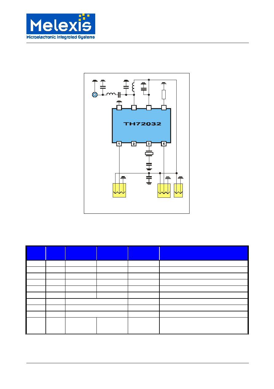
Test Circuit
Fig. 5: Test circuit for ASK with 50
matching network
5.1 Test circuit component list to Fig. 5
Part
Size
Value @
868.3 MHz
Value @
915 MHz
Tolerance
Description
CX1
0805
22 pF
22 pF
±
5%
XOSC capacitor, note 1
CM1
0805
2.2 pF
2.2 pF
±
5%
impedance matching capacitor
CM2
0805
4.7 pF
5.6 pF
±
5%
impedance matching capacitor
CM3
0805
68 pF
68 pF
±
5%
impedance matching capacitor
LT
0805
12 nH
10 nH
±
5%
output tank inductor, note 2
LM
0805
12 nH
10 nH
±
5%
impedance matching inductor, note 2
RPS
0805
see para. 4.6
±
10%
power-select resistor
CB0
0805
220 nF
±
10%
blocking capacitor
CB1
0603
330 pF
±
10%
blocking capacitor
XTAL
HC49/S
27.13438 MHz
fundamental
wave
28.59375 MHz
fundamental
wave
±
30ppm
calibration
±
30ppm temp.
crystal, C
L
= 12 pF, C
0, max
= 7 pF, R
1
= 40
Note 1: value depends on crystal parameters
Note 2: for high-power applications high-Q wire-wound inductors should be used
AS
KDT
A
RPS
OU
T
VEE
VC
C
PS
EL
EN
T
X
XTAL
RO
I
6
7
8
VC
C
GN
D
1 2
EN
T
X
GN
D
VC
C
1 2 3
DA
T
A
GN
D
VC
C
1 2 3
5
CX1
CM2
OUT
CM1
LT
n.
c
.
CM3
LM
CB1
CB0
TH72032
868/915MHz
ASK Transmitter
3901072032
Page 12 of 14
Data Sheet
Rev. 004
Feb./03
PR
ELI
MIN
AR
Y
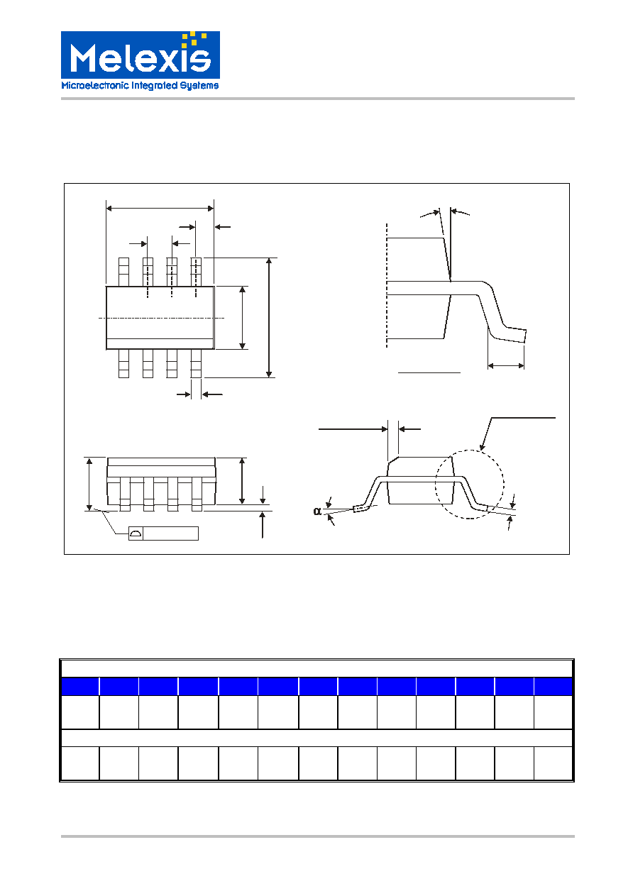
6
Package Information
Fig. 6: SOIC8 (Small Outline Integrated Circuit)
all Dimension in mm, coplanarity < 0.1mm
D
E
H
A
A1
A2
e
B
ZD
C
L
min
4.80
3.81
5.80
1.52
0.10
1.37
0.36
0.19
0.41
0°
max
4.98
3.99
6.20
1.72
0.25
1.57
1.27
0.46
0.53
0.25
1.27
8°
all Dimension in inch, coplanarity < 0.004"
min
0.189
0.150 0.2284 0.060 0.0040 0.054
0.014
0.075
0.016
0°
max
0.196
0.157 0.2440 0.068 0.0098 0.062
0.050
0.018
0.021
0.098
0.050
8°
e
D
8
1
ZD
H
E
B
A1
A2
A
7°
L
DETAIL - A
DETAIL - A
0.38 x 45°
(0.015x45°)
BSC
C
.10 (.004)

TH72032
868/915MHz
ASK Transmitter
3901072032
Page 13 of 14
Data Sheet
Rev. 004
Feb./03
PR
ELI
MIN
AR
Y
7
Reliability Information
Melexis devices are classified and qualified regarding suitability for infrared, vapor phase and wave soldering
with usual (63/37 SnPb-) solder (melting point at 183degC).
The following test methods are applied:
·
IPC/JEDEC J-STD-020A (issue April 1999)
Moisture/Reflow Sensitivity Classification For Nonhermetic Solid State Surface Mount Devices
·
CECC00802 (issue 1994)
Standard Method For The Specification of Surface Mounting Components (SMDs) of Assessed Quality
·
MIL 883 Method 2003 / JEDEC-STD-22 Test Method B102
Solderability
For all soldering technologies deviating from above mentioned standard conditions (regarding peak
temperature, temperature gradient, temperature profile etc) additional classification and qualification tests
have to be agreed upon with Melexis.
The application of Wave Soldering for SMD's is allowed only after consulting Melexis regarding assurance of
adhesive strength between device and board.
For more information on manufacturability/solderability see quality page at our website:
http://www.melexis.com/
8
ESD Precautions
Electronic semiconductor products are sensitive to Electro Static Discharge (ESD).
Always observe Electro Static Discharge control procedures whenever handling semiconductor products.
Your Notes

TH72032
868/915MHz
ASK Transmitter
3901072032
Page 14 of 14
Data Sheet
Rev. 004
Feb./03
PR
ELI
MIN
AR
Y
9
Disclaimer
Devices sold by Melexis are covered by the warranty and patent indemnification provisions appearing in its
Term of Sale. Melexis makes no warranty, express, statutory, implied, or by description regarding the
information set forth herein or regarding the freedom of the described devices from patent infringement.
Melexis reserves the right to change specifications and prices at any time and without notice. Therefore, prior
to designing this product into a system, it is necessary to check with Melexis for current information. This
product is intended for use in normal commercial applications. Applications requiring extended temperature
range, unusual environmental requirements, or high reliability applications, such as military, medical life-
support or life-sustaining equipment are specifically not recommended without additional processing by
Melexis for each application.
The information furnished by Melexis is believed to be correct and accurate. However, Melexis shall not be
liable to recipient or any third party for any damages, including but not limited to personal injury, property
damage, loss of profits, loss of use, interrupt of business or indirect, special incidental or consequential
damages, of any kind, in connection with or arising out of the furnishing, performance or use of the technical
data herein. No obligation or liability to recipient or any third party shall arise or flow out of Melexis' rendering
of technical or other services.
© 2002 Melexis NV. All rights reserved.
For the latest version of this document. Go to our website at
www.melexis.com
Or for additional information contact Melexis Direct:
Europe and Japan:
All other locations:
Phone: +32 1367 0495
Phone: +1 603 223 2362
E-mail: sales_europe@melexis.com
E-mail: sales_usa@melexis.com
QS9000, VDA6.1 and ISO14001 Certified