
MDT19C01
This specification are subject to be changed without notice. Any latest information please preview
http;//www.mdtic.com.tw
P.1 VER1.1
MDT19C01
1. General Description
This chip is the evaluation chip for MDT MPU
2. Features
u
ROM size can be set : 0.5K ,1K , 2K or 4 K words
u
RAM size can be set : 24, 40, 72, 136 bytes
u
37 single word instructions
u
Two operating voltage :
Vdd for MPU with range from 2.3 V ~ 6.3 V
Vcc
for memory and control interface circuit from 4.5V to 5.5V
u
Operating frequency : 0 ~ 20 MHz
u
Function compatible MDT MPU
u
I/O port can be set : 5, 12, 16, 20, 24 pins
u
Pull-up or pull-down resistors can be set by configuration registers
u
/HALT pin to control MPU operating at single step mode
u
Use 100 pin QFP package
3. Applications
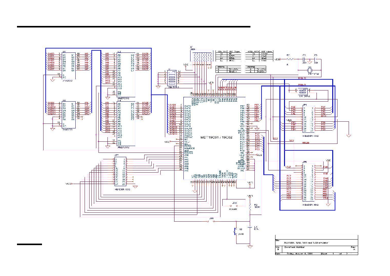
ICE for MDT1005/2005, MDT1010/2010, MDT1015/2015, MDT1020/2020
MDT1030, MDT80C01, MDT10C21, MDT10C22 MPU

MDT19C01
This specification are subject to be changed without notice. Any latest information please preview
http;//www.mdtic.com.tw
P.2 VER1.1
4. Pin Assignment

MDT19C01
This specification are subject to be changed without notice. Any latest information please preview
http;//www.mdtic.com.tw
P.3 VER1.1
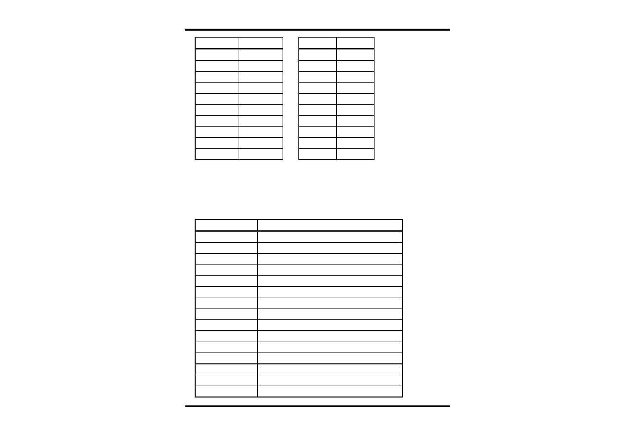
5. Pin Function Description
Pin Name
I/O
Function Description
PA0~PA7
I/O
Port A, TTL input level
PB0~PB7
I/O
Port B, TTL input level
PC0~PC7
I/O
Port C, TTL input level
AA0~AA7
O
RAM address bus
AD0~AD7
I/O
Data bus
/CE1
O
RAM chip enable
/CE2
O
External RAM chip enable
/RAMWR
O
RAM write enable
OAD0~OAD13
I/O
ROM address bus/Instruction bus
BGMODE
O
("1" = Background mode) ("0" = normal mode)
ALE
O
ROM address latch enable
/ROMOE
O
ROM output enable
RTCC
I
Real Time Clock/Counter, Schmitt Trigger input levels
/MCLR
I
Master Clear, Schmitt Trigger input levels
FNOP
O
Active at second cycle of two-cycle instructions
/HALT
I
Halt MPU function (with internal pull high)
HACK
O
Halt acknowledge
/RTSTP
I
Stop RTCC timer
/CONF
I
Select configuration registers
CLKOUT
O
T34 cycle clock
CLKT1
O
T1 cycle clock
CLKT3
O
T3 cycle clock
WDTCK
I
Watchdog clock input. To meet the basic time out
Period equals to 20ms (WDTCK x 512), the input
Frequency should be around 25.6KHZ
WDTCKO
O
Built-in watchdog clock output
OST1, OST0
I
Set oscillator setup time (V
dd
= 5V )
00 : WDTCK x 4 (150
s)
01 : WDTCK x 512 ( 20 ms)
10 : WDTCK x 1024 ( 40 ms)
11 : WDTCK x 2048 ( 80 ms)

MDT19C01
This specification are subject to be changed without notice. Any latest information please preview
http;//www.mdtic.com.tw
P.4 VER1.1
Pin Name
I/O
Function Description
OSC1
I
Oscillator input
OSC2
O
Oscillator output
/SLPO
O
Sleep function
OS1, OS0
I
Set oscillator type
00 : RC Oscillator
01 : LFXT Oscillator
10 : XTAL Oscillator
11 : HFXT Oscillator
/EPOR
I
External Power on reset
/PORO
O
Built-in power-on-reset output
WDTEN
I
Watchdog Timer control (`0' = Disable) (`1' = Enable)
/DISRAM
I
Internal RAM control (`0' = Disable) (`1' = Enable)
PEDEN
I
Power-edge detect control (`0' = Disable) (`1' =
Enable)
Vdd
I
Power supply for MPU
Vcc
I
+5V power for memory & control interface pins
Vss
I
Ground
6. Configuration Register
Address
Description
10
Set pull- down resister for PA
11
Set pull- up resister for PA
12
Set pull- down resister for PB
13
Set pull- up resister for PB
14
Set pull- down resister for PC
15
Set pull- up resister for PC
16
Set MPU PA PB PC I/O
17
Set MPU RAM, ROM size
18
Chip ID code (Read only)
19
General purpose register
1A
General purpose register
1B
General purpose register

MDT19C01
This specification are subject to be changed without notice. Any latest information please preview
http;//www.mdtic.com.tw
P.5 VER1.1
7. Power on reset
The power-on reset will be occurred while the power is applied to VDD or a low pulse is
detected form /EPOR pin. After power-on reset, this chip is in the background mode and
configuration registers are in the default states.
(A) Configuration registers
The /CONF = 0 or operating in background mode, the R10~R15 will change to configuration
Registers and a low pulse on /MCLR pin will not change this setting.
Register
Power-On Reset
10H : set pull-down resister for PA
0000 0000
11H : set pull-up resister for PA
0000 0000
12H : set pull-down resister for PB
0000 0000
13H : set pull-up resister for PB
0000 0000
14H : set pull-down resister for PC
0000 0000
15H : set pull-up resister for PC
0000 0000
16H : set MPU PA PB PC I/O
set pull-up resister for RTCC, /MCLR
set pull-down resister for RTCC,/MCLR
0000 0000
17H : set MPU RAM, ROM size
0000 0001
18H : Chip ID code (Read only)
0000 0001
19H : General purpose register
0000 0000
1AH : General purpose register
0000 0000
1BH : General purpose register
0000 0000
Note : Disable
"0" ; Enable
"1"

MDT19C01
This specification are subject to be changed without notice. Any latest information please preview
http;//www.mdtic.com.tw
P.6 VER1.1
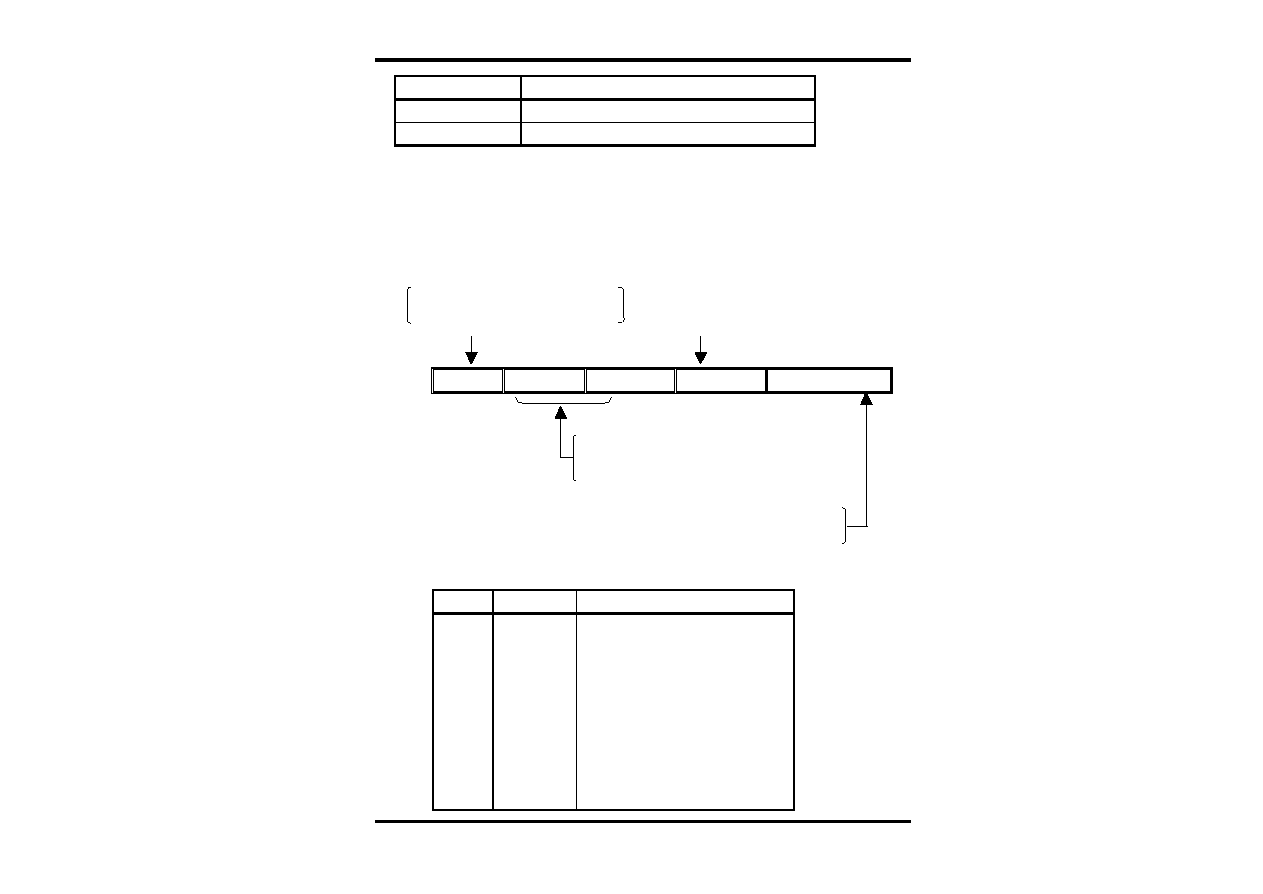
(B) Register 16H
Select port A I/O
00 : 4 I/O
01 : 8 I/O
Select port C I/O 1X : 0 I/O
RTCC pull-up 0 : 8 I/O
/MCLR pull-up 1 : 0 I/O
b7
b6
b5
b4
b3
b2
b1
b0
/MCLR pull-down
RTCC pull-down Select port B I/O
0 : 8 I/O
1 : 5 I/O
(C) Register 17H
Set RAM Select operating mode
Read only "0" 0 : All internal RAM 0 : normal mode
1 : 90~FF external RAM 1 : background mode
b7
b6
b5
b4
b3
b2
b1
b0
Select ROM size Select RAM size
00 : 0.5K 00 : 24 byte
01 : 1K 01 : 40 byte
10 : 2K 10 : 72 byte
11 : 4K 11 : 128 byte
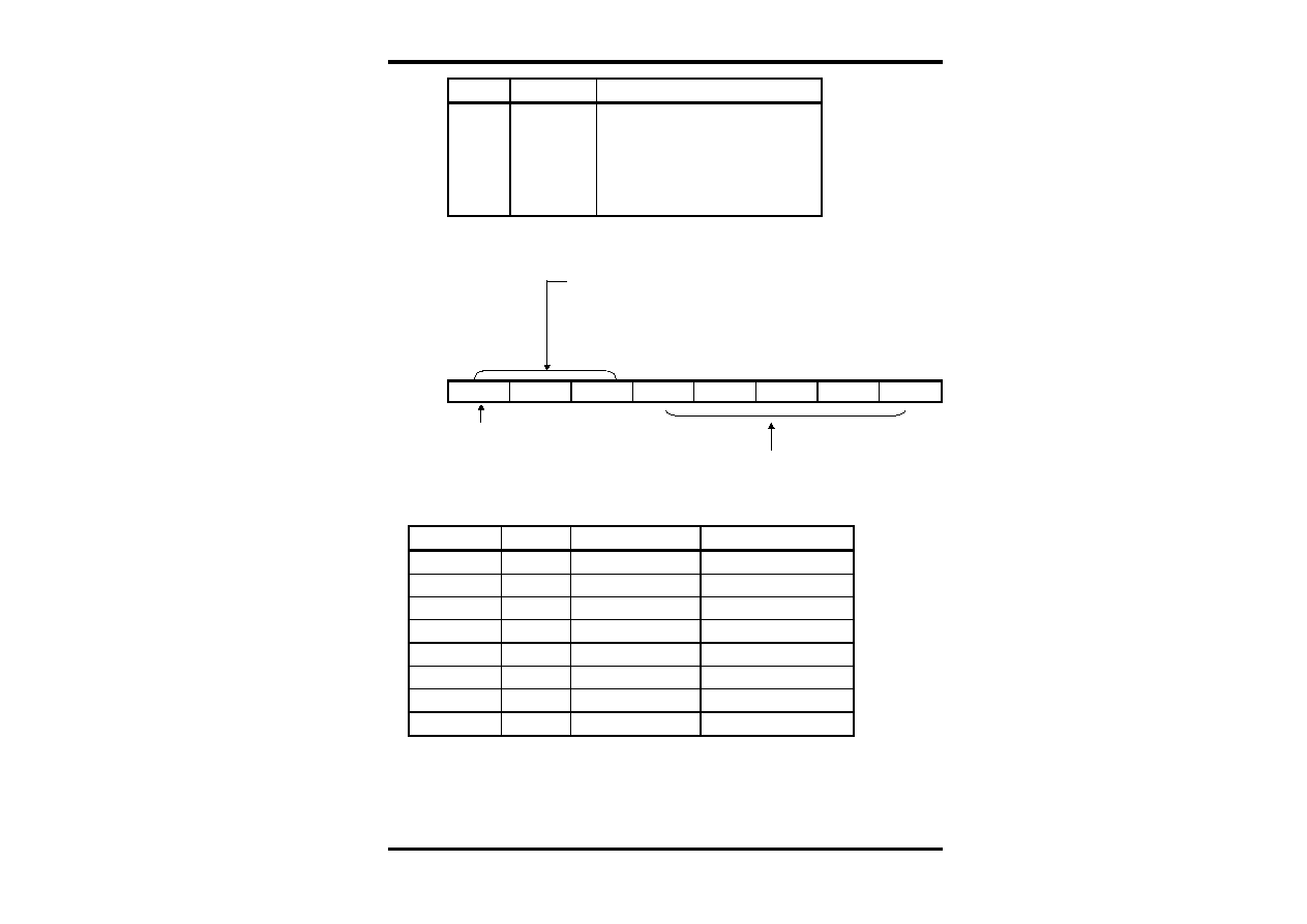
8. Set MPU
Set SPECIAL RAM, ROM & I/O
17H set
ROM, RAM
16H set PC, PB, PA
xx00 x000
0.5K, 24B
---- 0000 8 8 4
xx00 x010
0.5K, 40B
---- 0001 8 8 8
xx00 x100
0.5K, 72B
---- 0010 8 8 0
xx00 #110
0.5K, 136B
---- 0011 8 8 0
xx01 x000
1K, 24B
---- 0100 8 5 4
xx01 x010
1K, 40B
---- 0101 8 5 8
MDT19C01
This specification are subject to be changed without notice. Any latest information please preview
http;//www.mdtic.com.tw
P.7 VER1.1
17H set
ROM, RAM
16H set PC, PB, PA
xx01 x100
1K, 72B
---- 0110 8 5 0
xx01 #110
1K, 136B
---- 0111 8 5 0
xx10 x000
2K, 24B
---- 1000 0 8 4
xx10 x010
2K, 40B
---- 1001 0 8 8
xx10 x100
2K, 72B
---- 1010 0 8 0
xx10 #110
2K, 136B
---- 1011 0 8 0
xx11 x000
4K, 24B
---- 1100 0 5 4
xx11 x010
4K, 40B
---- 1101 0 5 8
xx11 x100
4K, 72B
---- 1110 0 5 0
xx11 #110
4K, 136B
---- 1111 0 5 0
Note : ` x '
unused, ` - ` is set RTCC, /MCLR pull-up or down
` # '
` 0 ' RAM all internal , ` # '
` 1 ' 90 ~ FF external RAM
9. Normal mode Memory Map
Register Map
Address
Description
00
Indirect Addressing Register
01
RTCC
02
PC
03
STATUS
04
MSR
05
Port A
06
Port B
07
Port C
08~0F
Internal RAM, General Purpose Register
10~1F
Internal Memory Select Register (24 bytes)
30~3F
Internal Memory Select Register (40 bytes)
50~5F
Internal Memory Select Register
70~7F
Internal Memory Select Register (72 bytes)
90~9F
Internal Memory Select Register
B0~BF
Internal Memory Select Register
MDT19C01
This specification are subject to be changed without notice. Any latest information please preview
http;//www.mdtic.com.tw
P.8 VER1.1
Address
Description
D0~DF
Internal Memory Select Register
F0~FF
Internal Memory Select Register (136 bytes)
(1) IAR ( Indirect Address Register) : R0
(2) RTCC (Real Time Counter/Counter Register) : R1
(3) PC (Program Counter) : R2
Write PC, JUMP, CALL --- from SATUS b7
LJUMP, LCALL --- from SATUS b7 Write PC, CALL --- always 0
RTIW, RET --- from STACK LJUMP, JUMP, LCALL --- from instruction word
RTIW, RET --- from STACK
A11
A10
A9
A8
A7~A0
Write PC, JUMP, CALL --- from SATUS b6 b5
LJUMP, LCALL --- from instruction word
RTIW, RET --- from STACK
Write PC --- from ALU
LJUMP, JUMP, LCALL, CALL --- from instruction word
RTIW, RET --- from STACK
(4) STATUS (Status register) : R3
Bit
Symbol
Function
0
1
2
3
4
7
--
5
C
HC
Z
PF
TF
page
Carry bit
Half Carry bit
Zero bit
Power loss Flag bit
Time overflow Flag bit
Page select bit :(ROM : 4.0 K)
000 : 000H --- 1FFH
001 : 200H --- 3FFH
010 : 400H --- 5FFH
MDT19C01
This specification are subject to be changed without notice. Any latest information please preview
http;//www.mdtic.com.tw
P.9 VER1.1
Bit
Symbol
Function
011 : 600H --- 7FFH
100 : 800H --- 9FFH
101 : A00H --- BFFH
110 : C00H --- DFFH
111 : E00H --- FFFH
(5) MSR (Memory Select Register) : R4
Memory Select Register :
000 : 10~1F 100 : 90~9F
001 : 30~3F 101 : B0~BF
010 : 50~5F 110 : D0~DF
011 : 70~7F 111 : F0~FF
b7
b6
b5
b4
b3
b2
b1
b0
Always Read "1"
If RAM not set 136 Bytes
Indirect Addressing Mode
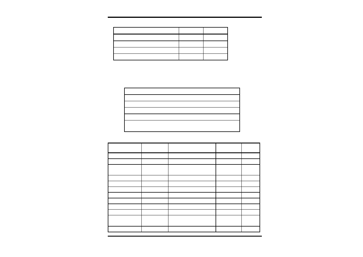
10. Reset Condition for all Registers
Register
Address
Power-On Reset
/MCLR or WDT Reset
IAR
00h
RTCC
01h
xxxx xxxx
uuuu uuuu
PC
02h
1111 1111
1111 1111
STATUS
03h
0001 1xxx
000# #uuu
MSR
04h
100x xxxx
100u uuuu
PORT A
05h
xxxx xxxx
uuuu uuuu
PORT B
06h
xxxx xxxx
uuuu uuuu
PORT C
07h
xxxx xxxx
uuuu uuuu
Note
u
unchanged
x
unknown
-
unimplemented
read as "0"
#
value depends on the condition of the following table
MDT19C01
This specification are subject to be changed without notice. Any latest information please preview
http;//www.mdtic.com.tw
P.10 VER1.1
Condition
Status
bit 4 Status
bit 3
/MCLR reset (not during SLEEP)
u
u
/MCLR reset during SLEEP
1
0
WDT reset (not during SLEEP)
0
1
WDT reset during SLEEP
0
0
11. Halt state
The MPU can be halt by HALT instruction or pull /HALT pin to low. The halt state are
listed below
1. Stop program counter
2. Stop watchdog clock
3. Stop RTCC if clock source is internal clock
4. Set HACK to high
5. Force the next operation to be NOP
6. Software Halt can only be released by applying a negative pulse
(at least one instruction cycle long) to /HALT
12. Instruction Set
Instruction Code
Mnemonic
Operands
Function
Operating
Status
010000 00000000 NOP
No operation
None
010000 00000001 CLRWT
Clear Watchdog timer
0
WT TF
PF
010000 00000010 SLEEP
Sleep mode
0
WT
stop OSC
TF
PF
010000 00000011 TMODE
Load W to TMODE register
W
TMODE
None
010000 00000100 RET
Return Stack
PC
None
010000 00001000 HALT
Halt MPU
None
010000 00000rrr CPIO R
Control I/O port register
W
CPIO r
None
010001 1rrrrrrr
STWR R
Store W to register
W
R
None
011000 trrrrrrr
LDR R
t
Load register R
t
Z
111010 iiiiiiii
LDWI I
Load immediate to W I
W
None
010111 trrrrrrr
SWAPR R
t Swap halves register [R(0~3)
R(4~7)]
t
None
011001 trrrrrrr
INCR R
t
Increment register
R + 1
t
Z

MDT19C01
This specification are subject to be changed without notice. Any latest information please preview
http;//www.mdtic.com.tw
P.11 VER1.1
Instruction Code
Mnemonic
Operands
Function
Operating
Status
011010 trrrrrrr
INCRSZ R
t Increment register
skip if
zero
R + 1
t
None
011011 trrrrrrr
ADDWR R
t Add W and register
W + R
t
C
HC
Z
011100 trrrrrrr
SUBWR R, t Subtract W from register
R
W
t
(R+/W+1
t)
C, HC, Z
011101 trrrrrrr
DECR R, t
Decrement register
R
1
t
Z
011110 trrrrrrr
DECRSZ R, t Decrement register, skip if
zero
R
1
t
None
010010 trrrrrrr
ANDWR R, t AND W and register
R
W
t
Z
110100 iiiiiiii
ANDWI i
AND W and immediate
i
W
W
Z
010011 trrrrrrr
IORWR R, t
Inclu. OR W and register
R
W
t
Z
110101 iiiiiiii
IORWI i
Inclu. OR W and immediate
i
W
W
Z
010100 trrrrrrr
XORWR R, t Exclu. OR W and register
R
W
t
Z
110110 iiiiiiii
XORWI i
Exclu. OR W and immediate i
W
W
Z
011111 trrrrrrr
COMR R, t Complement register /R
t
Z
010110 trrrrrrr
RRR R, t
Rotate right register
R(n)
R(n-1),
C
R(7),
R(0)
C
C
010101 trrrrrrr
RLR R, t
Rotate left register
R(n)
r(n+1),
C
R(0),
R(7)
C
C
010000 1xxxxxxx CLRW
Clear working register
0
W
Z
010001 0rrrrrrr
CLRR R
Clear register 0
R
Z
0000bb brrrrrrr
BCR R, b
Bit clear 0
R(b)
None
0010bb brrrrrrr
BSR R, b
Bit set 1
R(b)
None
0001bb brrrrrrr
BTSC R, b
Bit Test, skip if clear
Skip if R(b)=0 None
0011bb brrrrrrr
BTSS R, b
Bit Test, skip if set
Skip if R(b)=1 None
100nnn nnnnnnnn LCALL n
Long CALL subroutine
n
PC,
PC+1
Stack
None
101nnn nnnnnnnn LJUMP n
Long JUMP to address
n
PC
None
110000 nnnnnnnn CALL n
Call subroutine n
PC,
PC+1
Stack
None
110001 iiiiiiii
RTIW i
Return, place immediate to W Stack
PC,
i
W
None
11001n nnnnnnnn JUMP n
JUMP to address n
PC
None
Note :

MDT19C01
This specification are subject to be changed without notice. Any latest information please preview
http;//www.mdtic.com.tw
P.12 VER1.1
HALT is only available for MDT19C01 only.
W
: Working register b :
Bit position
WT
: Watchdog timer
t :
Target
TMODE : TMODE mode register
0
:
Working register
CPIO
: Control I/O port register
1 :
General register
TF
: Timer overflow flag
R :
General register address
PF
: Power loss flag
C :
Carry flag
PC
: Program Counter
HC :
Half carry
OSC
: Oscillator
Z
:
Zero flag
Inclu.
: Inclusive `
'
/
:
Complement
Exclu.
: Exclusive `
'
x
:
Don't care
AND
: Logic AND `
'
i
:
Immediate data ( 8 bits )
n
:
Immediate address

MDT19C01
This specification are subject to be changed without notice. Any latest information please preview
http;//www.mdtic.com.tw
P.13 VER1.1
13. Timing diagram
T 1
T 2
T 3
T 4
AA0-AA7
10ns
20ns
AD0-AD7
(READ)
AD0-AD7
(WRITE)
/CE1,/CE 2
/RAMWR
20ns
OAD0-OAD13
ADDRESS
DATA
20ns
ALE
10ns
/ROMOE
20ns
/HALT
20ns
HACK
CLKOUT
CLKT1
CLKT3
FNOP
MDT19C01
This specification are subject to be changed without notice. Any latest information please preview http;//www.mdtic.com.tw
P.1
VER1.1
14. Application circuit