Features
l
Low Reverse Recovery Time
l
Low Reverse Capacitance
l
Low Forward Voltage Drop
l
Guard Ring Construction for Transient Protection
Mechanical Data
l
Case: DO-35, Glass
l
Terminals: Solderable per MIL-STD-202, Method 208
l
Polarity: Indicated by Cathode Band
Maximum Ratings @ 25
o
C Unless Otherwise Specified
Characteristic
Symbol
SD103A
SD103B
SD103C
Peak Repetitive Reverse Voltage
V
RRM
Working Peak Reverse Voltage
V
RWM
40V
30V
20V
DC Blocking Voltage
V
R
RMS Reverse Voltage
V
R(RMS)
28V
21V
14V
Maximum sigle cycle surge 60Hz
sine wave
I
FSM
Power Dissipation(Note 1)
P
d
Thermal Resistance, Junction to
Ambient
R
Junction Tmperature
T
j
Operation/Storage Temp. Range
T
STG
-55 to +150
o
C
300K/W
400mW
15A
125
o
C
Electrical Characteristics @ 25
o
C Unless Otherwise Specified
Charateristic Symbol Type Max Test Condition
SD103A
5.0uA
V
R
=30V
Leakage SD103B
I
R
-----
5.0uA
V
R
=20V
Current SD103C
5.0uA
V
R
=10V
Maximum Forward
V
F M
-----
0.37V
I
F
=20mA
Voltage Drop
0.60V
I
F
=200mA
Junction Capacitance
Cj
50pF
-----
V
R
=0V, f=1.0MHz
Reverse Recovery Time
t
rr
10ns
-----
I
F
=I
R
=50mA, recover to
200mA/0.1I
R
Note
: 1. Valid provided that electrodes are kept at ambient temperature
SD103A
THRU
SD103C
Small Signal
Schottky Diodes
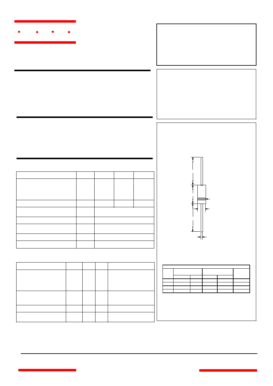
DO-35
DIMENSIONS
INCHES
MM
DIM
MIN
MAX
MIN
MAX
NOTE
A
---
.166
---
4.2
B
---
.079
---
2.00
C
---
.020
---
.52
D
1.000
---
25.40
---
A
B
C
D
D
Cathode
Mark
www.
mccsemi
.com
omponents
21201 Itasca Street Chatsworth
!"#
$
% !"#
M C C
I (mA)
F
T = 25 C
j
A
A
mA
ms
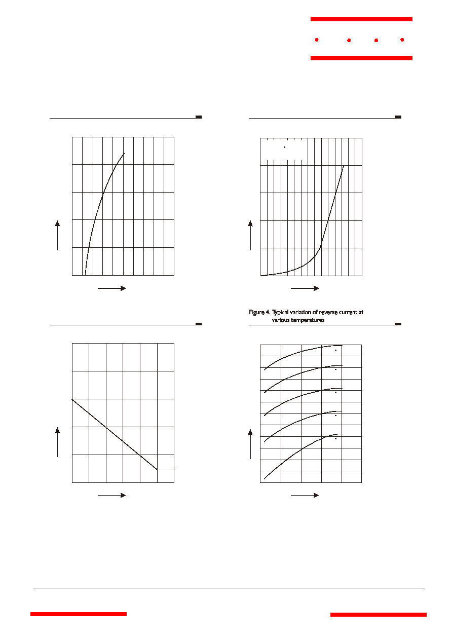
Figure 1. Typical variation of forward current vs. Forward.
Voltage for primary conduction through the
schottky barrier
Figure 2. Typical high current forward
conduction curve t =300ms,duty cycle=2%
p
V
F
V
F
V
R
I
F
I
F
I
F
Figure 3. Typical non repetitive forward surge
current versus pulse width
t
p
I
F
SD103A thru SD103C
M C C
www.
mccsemi
.com
V
pF
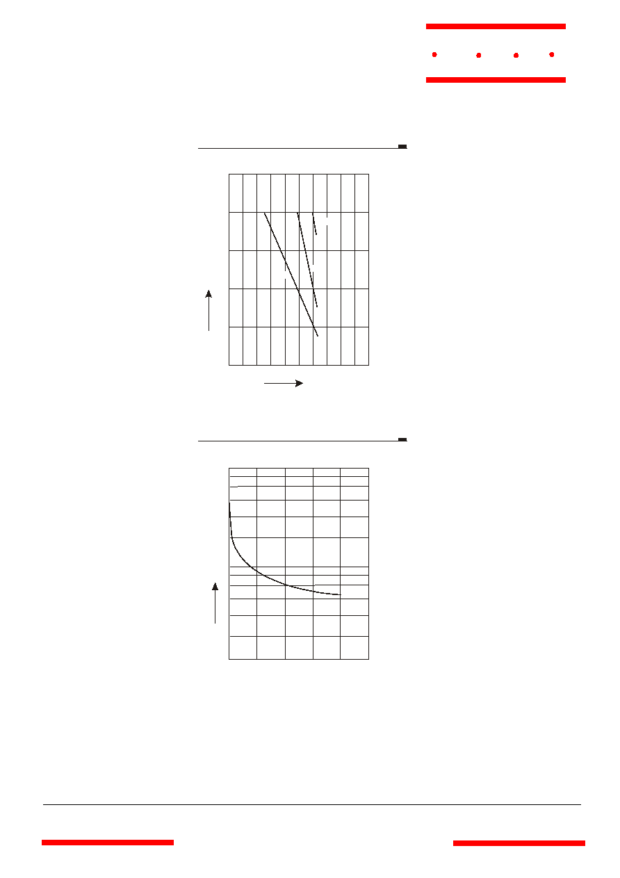
Figure 5. Blocking deration versus
at various average forward currents
temperature
T
A
V
R
Figure 6. Typical capacitance versus
reverse voltage
C
tot
SD103A thru SD103C
M C C
www.
mccsemi
.com