1
Memory
All data sheets are subject to change without notice
(858) 503-3300 - Fax: (858) 503-3301 - www.maxwell.com
CMOS Logic Hex
54HC4049
©2001 Maxwell Technologies.
All rights reserved.
Inverting Buffers
12.20.01 Rev1
1000589
54HC4049
F
EATURES
:
· High speed CMOS logic hex inverting Buffers
· R
AD
-P
AK
® radiation hardened against natural space radia-
tion
· Single Event Effects:
- SEL: > 120 MeV/mg/cm2
· Total dose hardness:
· - > 100 Krad (Si), depending upon space mission
· Package:
-16 Pin R
AD
-P
AK
® Flat Pack
· Typical propagation delay:
- 6ns at V
CC
= 5V, C
L
= 15pF, TA = 25°C
· High-to-Low voltage level converter for up to V
I
= 16V
· Fanout (over temperature range)
-10 LSTTL loads (Standard Outputs)
-15 LSTTL loads (Bus Driver Outputs)
· Balanced propagation delay and transition times
· Significant power reduction compared to LSTTL logic ICs
· 2V to 6V operation
· High noise immunity
· -N
IL
= 30%, N
IH
= 30% of V
CC
at V
CC
= 5V
D
ESCRIPTION
:
Maxwell Technologies' 54HC4049 high speed CMOS Logic
Hex Inverting Buffers features a greater than 100 krad(Si) total
dose tolerance, depending upon space misssion. These parts
have a modified input protection structure that enables them
to be used as logic level translators which will convert high-
level logic to a low-level logic while operating off the low-level
logic supply. For example, 15V input pulse levels can be
down-converted to 0V to 5V logic levels. The modified input
protection structure protects the input from negative electro-
static discharge. The 54HC4049 can be used as simple buff-
ers or inverters without level translation.
Maxwell Technologies' patented R
AD
-P
AK
® packaging technol-
ogy incorporates radiation shielding in the microcircuit pack-
age. It eliminates the need for box shielding while providing
the required radiation shielding for a lifetime in orbit or space
mission. In a GEO orbit, R
AD
-P
AK
provides greater than 100
krad (Si) radiation dose tolerance. This product is available
with screening up to Class S.
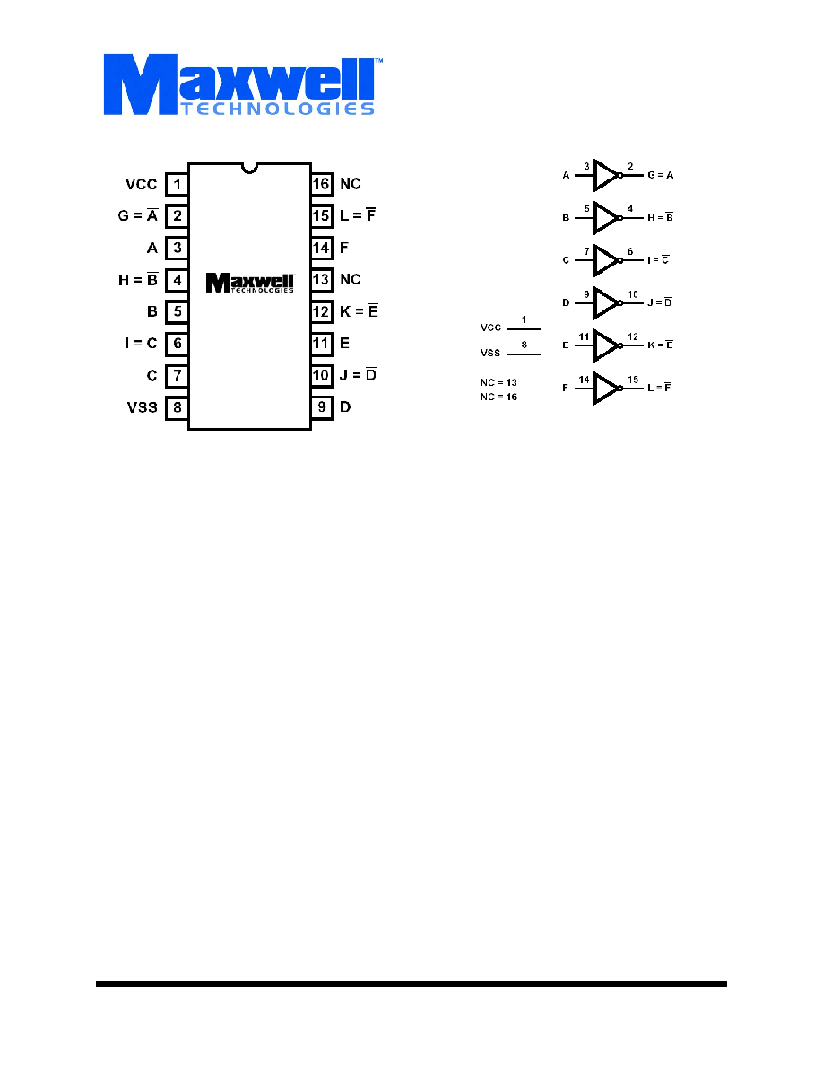
Logic Diagram

Memory
2
All data sheets are subject to change without notice
©2001 Maxwell Technologies.
All rights reserved.
CMOS Logic Hex Inverting Buffers
54HC4049
12.20.01 Rev1
1000589
T
ABLE
1. 54HC4049 P
INOUT
D
ESCRIPTIONS
P
IN
S
YMBOL
D
ESCRIPTION
1
V
CC
Power supply
8
V
SS
Ground
13, 16
NC
Not Connected
3, 5, 7, 9, 11, 14
A - F
Inputs
2
G = A
Inverted Output
4
H = B
Inverted Output
6
I = C
Inverted Output
10
J = D
Inverted Output
12
K = E
Inverted Output
15
L = F
Inverted Output
T
ABLE
2. 54HC4049 A
BSOLUTE
M
AXIMUM
R
ATINGS
P
ARAMETER
S
YMBOL
M
IN
M
AX
U
NIT
Storage Temperature
T
S
-65
150
°C
Operating Temperature Range
T
A
-55
125
°C
DC Supply Voltage
V
CC
-0.5
7.0
V
DC Input Diode Current
For V
I
< -0.5V or V
I
> V
CC
+0.5V
I
IK
-20
+20
mA
DC Output Diode Current
For V
O
< -0.5V or V
O
> V
CC
+0.5V
I
OK
-20
+20
mA
DC Output Source or Sink Current per Output Pin
For V
O
> -0.5V or V
O
< V
CC
+0.5V
I
O
-25
+25
mA
DC V
CC
or Ground Current
I
CC
or I
GND
-50
+50
mA
T
ABLE
3. D
ELTA
L
IMITS
P
ARAMETER
V
ARIATION
I
CC
±10% of specified value in Table 5

Memory
3
All data sheets are subject to change without notice
©2001 Maxwell Technologies.
All rights reserved.
CMOS Logic Hex Inverting Buffers
54HC4049
12.20.01 Rev1
1000589
T
ABLE
4. 54HC4049 R
ECOMMENDED
O
PERATING
C
ONDITIONS
P
ARAMETER
S
YMBOL
M
IN
M
AX
U
NIT
Supply Voltage
V
CC
2
6
V
DC Input or output Voltage
V
I
, V
O
0
V
CC
V
Input Rise and Fall Time
2V
4.5V
6V
--
1000
500
400
ns
Temperature Range
T
A
-55
125
°C
T
ABLE
5. 54HC4049 DC E
LECTRICAL
C
HARACTERISTICS
(V
CC
= 5V ±10%, T
A
= -55
TO
125°C,
UNLESS
OTHERWISE
SPECIFIED
)
P
ARAMETER
S
YMBOL
T
EST
C
ONDITIONS
M
IN
M
AX
U
NIT
High Level Output Voltage
CMOS Loads
V
OH
V
I
= V
IH
or V
IL
, I
O
= -0.02mA
V
CC
= 2V
V
CC
= 4.5V
V
CC
= 6V
1.9
4.4
5.9
--
--
--
V
High Level Output Voltage
TTL Loads
V
I
= V
IH
or V
IL
, I
O
= -4mA
V
CC
= 4.5V
+25°C
3.98
--
-55 to 125°C
3.7
--
V
I
= V
IH
or V
IL
, I
O
= -5.2mA
V
CC
= 6V
+25°C
5.48
--
-55 to 125°C
5.2
--
Low Level Output Voltage
CMOS Loads
V
OL
V
I
= V
IH
or V
IL
, I
O
= -0.02mA
V
CC
= 2V
V
CC
= 4.5V
V
CC
= 6V
0.1
0.1
0.1
V
Low Level Output Voltage
TTL Loads
V
I
= V
IH
or V
IL
, I
O
= 4mA
V
CC
= 4.5V
+25°C
0.26
--
-55 to 125°C
0.4
V
I
= V
IH
or V
IL
, I
O
= 5.2mA
V
CC
= 6V
+25°C
0.26
--
-55 to 125°C
0.4
High Level Input Voltage
V
IH
V
CC
= 2V
V
CC
= 4.5V
V
CC
= 6V
1.5
3.15
4.2
--
--
--
V
Low Level Input Voltage
V
IL
V
CC
= 2V
V
CC
= 4.5V
V
CC
= 6V
--
--
--
0.5
1.35
1.8
V
Input Leakage Current
I
I
V
CC
= 6V, V
I
= V
CC
or GND
+25°C
--
±0.1
µA
-55 to 125°C
--
±1
V
CC
= 6V, V
I
= 15V
+25°C
--
±0.5
-55 to 125°C
--
±5

Memory
4
All data sheets are subject to change without notice
©2001 Maxwell Technologies.
All rights reserved.
CMOS Logic Hex Inverting Buffers
54HC4049
12.20.01 Rev1
1000589
Quiescent Device Current
I
CC
V
I
= V
CC
or GND, I
O
= 0mA
V
CC
= 6V
+25°C
--
2
µA
-55 to 125°C
--
40
T
ABLE
6. 54HC4049 AC E
LECTRICAL
C
HARACTERISTICS
(V
CC
= 5V ±10%, T
A
= -55
TO
125°C,
UNLESS
OTHERWISE
SPECIFIED
)
P
ARAMETER
S
YMBOL
T
EST
C
ONDITION
M
IN
M
AX
U
NIT
Propogation Delay
nA to nY
t
PLH,
t
PHL
C
L
= 50pF
V
CC
= 2V
+25°C
--
85
ns
-55 to 125°C
--
130
V
CC
= 4.5V
+25°C
--
17
-55 to 125°C
--
26
V
CC
= 6V
+25°C
--
14
-55 to 125°C
--
22
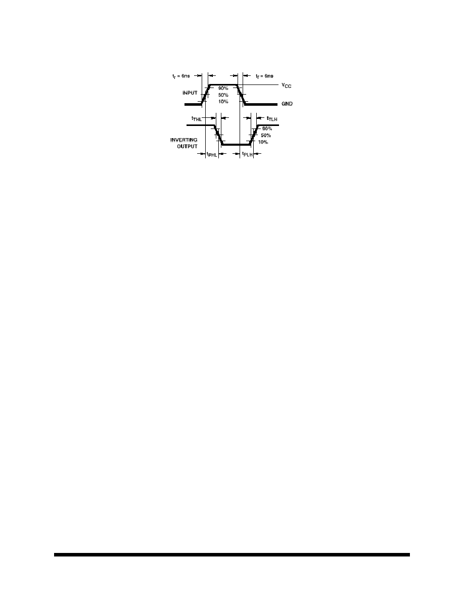
Transition Times
(Figure 1)
t
TLH,
t
THL
C
L
= 50pF
V
CC
= 2V
+25°C
--
75
ns
-55 to 125°C
--
110
V
CC
= 4.5V
+25°C
--
15
-55 to 125°C
--
22
V
CC
= 6V
+25°C
--
13
-55 to 125°C
--
19
T
ABLE
7. 54HC4049 C
APACITANCE1
1. Guaranteed by design.
P
ARAMETER
S
YMBOL
T
EST
C
ONDITIONS
T
YP
U
NIT
Input Capacitance
C
I
10
pF
Power Dissipation Capacitance
2, 3
2. C
PD
is used to determine the dynamic power consumption, per gate.
3. P
D
= V
CC
2
fi (C
PD
+ C
L
) where fi = Input Frequency, C
L
= Output Load Capacitance, V
CC
= Supply Voltage.
C
PD
V
CC
= 5V
35
pF
T
ABLE
5. 54HC4049 DC E
LECTRICAL
C
HARACTERISTICS
(V
CC
= 5V ±10%, T
A
= -55
TO
125°C,
UNLESS
OTHERWISE
SPECIFIED
)
P
ARAMETER
S
YMBOL
T
EST
C
ONDITIONS
M
IN
M
AX
U
NIT
Memory
5
All data sheets are subject to change without notice
©2001 Maxwell Technologies.
All rights reserved.
CMOS Logic Hex Inverting Buffers
54HC4049
12.20.01 Rev1
1000589
F
IGURE
1. T
RANSITION
T
IMES
AND
P
ROPOGATION
D
ELAY
T
IMES
, C
OMBINATION
L
OGIC
Memory
6
All data sheets are subject to change without notice
©2001 Maxwell Technologies.
All rights reserved.
CMOS Logic Hex Inverting Buffers
54HC4049
12.20.01 Rev1
1000589
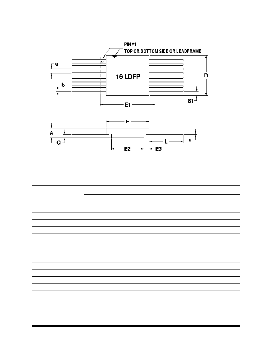
F16-01
Note: All dimensions in inches
16-P
IN
R
AD
-P
AK
® F
LAT
P
ACKAGE
S
YMBOL
D
IMENSION
M
IN
N
OM
M
AX
A
0.115
0.135
0.150
b
0.015
0.017
0.019
c
0.004
0.005
0.007
D
0.407
0.415
0.423
E
0.275
0.280
0.285
E1
--
--
0.500
E2
0.150
0.156
0.162
E3
0.030
0.062
--
e
0.050 BSC
L
0.325
0.335
0.345
Q
0.020
0.033
0.045
S1
0.005
0.024
0.045
N
16

Memory
7
All data sheets are subject to change without notice
©2001 Maxwell Technologies.
All rights reserved.
CMOS Logic Hex Inverting Buffers
54HC4049
12.20.01 Rev1
1000589
Important Notice:
These data sheets are created using the chip manufacturer's published specifications. Maxwell Technologies verifies
functionality by testing key parameters either by 100% testing, sample testing or characterization.
The specifications presented within these data sheets represent the latest and most accurate information available to
date. However, these specifications are subject to change without notice and Maxwell Technologies assumes no
responsibility for the use of this information.
Maxwell Technologies' products are not authorized for use as critical components in life support devices or systems
without express written approval from Maxwell Technologies.
Any claim against Maxwell Technologies must be made within 90 days from the date of shipment from Maxwell Tech-
nologies. Maxwell Technologies' liability shall be limited to replacement of defective parts.
Memory
8
All data sheets are subject to change without notice
©2001 Maxwell Technologies.
All rights reserved.
CMOS Logic Hex Inverting Buffers
54HC4049
12.20.01 Rev1
1000589
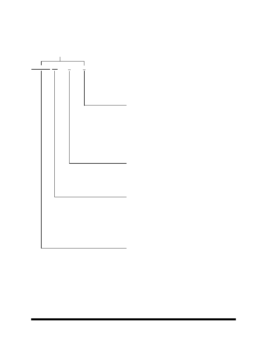
Product Ordering Options
Model Number
Feature
Option Details
54HC4049 RP
F
X
Screening Flow
Package
Radiation Feature
Base Product
Nomenclature
Monolithic
S = Maxwell Class S
B = Maxwell Class B
E = Engineering (testing @ +25°C)
I = Industrial (testing @ -55°C,
+25°C, +125°C)
F = Flat Pack
RP = R
AD
-P
AK
® package
CMOS Logic Hex Inverting Buffers