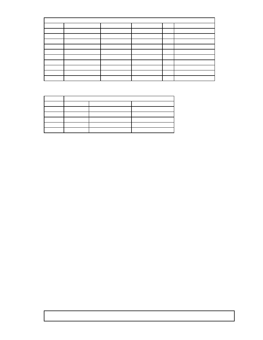
SCOPE: PRECISION REFERENCE +5 VOLT ADJUSTABLE OUTPUT
Device Type Generic Number
03
REF02A(x)/883B
04
REF02(x)/883B
Case Outline(s). The case outlines shall be designated in Mil-Std-1835 and as follows:
Outline Letter Mil-Std-1835 Case Outline Package Code
MAXIM SMD
Z P GDIP1-T8 or CDIP2-T8 8 LEAD CERDIP J8
J G MACY1-X8 8 LEAD CAN G99
RC 2 CQCC1-N20
20 PIN LCC
L20
Absolute Maximum Ratings
Supply Voltage V
DD
to GND .................................................................................. 40V
Output Short Circuit Duration (to GND or V
IN
) .............................................. Indefinite
Lead Temperature (soldering, 10 seconds) .............................................................. +300
°
C
Storage Temperature ................................................................................. -65
°
C to +150
°
C
Continuous Power Dissipation .............................................................................T
A
=
+
70
°
C
8 lead CERDIP(derate 8.0mW/
°
C above +70
°
C) .................................................... 640mW
8 pin CAN (derate 6.67mW/
°
C above +70
°
C)......................................................... 533mW
20 Pin LCC (derate 9.09mW/
°
C above +70
°
C)........................................................ 727mW
Junction Temperature T
J
....................................................................................... +150
°
C
Thermal Resistance, Junction to Case,
JC:
Case Outline 8 lead CERDIP................................................................... 55
°
C/W
Case Outline 8 lead CAN ........................................................................ 45
°
C/W
Case Outline 20 Pin LCC ........................................................................ 20
°
C/W
Thermal Resistance, Junction to Ambient,
JA:
Case Outline 8 lead CERDIP................................................................. 125
°
C/W
Case Outline 8 lead CAN ...................................................................... 150
°
C/W
Case Outline 20 Pin LCC ...................................................................... 110
°
C/W
Recommended Operating Conditions.
V
OUT
@ 25
°
C for device 03 ............................................................................ 5V
±
15mV
V
OUT
@ 25
°
C for device 04 ............................................................................ 5V
±
25mV
Ambient Operating Range (T
A
) ........................................................... -55
°
C to
+
125
°
C
Stresses beyond those listed under "Absolute Maximum Ratings" may cause permanent damage to the device.
These are stress ratings only, and functional operation of the device at these or any other conditions beyond
those indicated in the operational sections of the specifications is not implied. Exposure to absolute maximum
rating conditions for extended periods may affect device reliability.
----------------------------
Electrical Characteristics of REF02 & 02A/883B
19-0346
Rev. C
for SMD 85514
Page 2 of
6
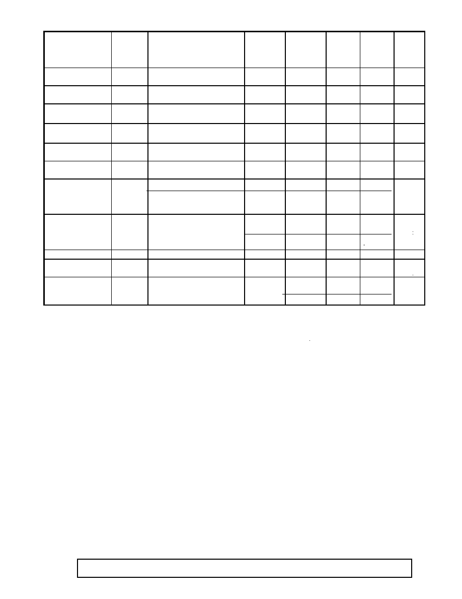
TABLE 1 ELECTRICAL TESTS
TEST
Symbol
CONDITIONS
-55
°
C
T
A
+125
°
C
V
DD
=+15V, V
IN
=+15V
Unless otherwise specified
Group A
Subgroup
Device
type
Limits
Min
Limits
Max
Units
Quiescent Supply
Current
I
IN
No load
1
2,3
All
1.4
2.0
mA
Output Adjustment
Range
V
TRIM
R
P
=10k
1
All
-3.0
+3.0 %
Output Voltage
V
O
I
L
=0mA
1
2,3
03
4.985
4.978
5.015
5.022
V
Output Voltage
V
O
I
L
=0mA
1
2,3
04
4.975
4.953
5.025
5.047
V
Short Circuit
Current
I
SC
V
O
=0
1
All
+15
+60 mA
Sink Current
I
S
1
All
-0.3
mA
Load Regulation
NOTE 1
LD reg
I
L
=0 to 10mA
I
L
=0 to 8mA
1
2,3
All
03
04
0.010
0.012
0.015
%/mA
Line Regulation
NOTE 1
LN reg
V
IN
=8V to 33V
1
2,3
03
04
All
0.010
0.012
0.015
%/V
Load Current
I
L
NOTE 2
1
All
10
mA
Output Voltage
Noise
e
np-p
0.1Hz to 10Hz
4
All
100
µ
Vp-p
Output Voltage
Temperature
Coefficient
TCVo
NOTE 3
7,,8
03
04
±
8.5
±
25
ppm/
°
C
NOTE 1: Line and Load Regulation specifications include the effect of self-heating.
NOTE 2: Minimum of 10mA load current guaranteed by load regulation test.
NOTE 3: V
MAX
-V
MIN
(-55
°
C to +125
°
C)1x10
6
TCV
O
= ----------------- x ----------------------------------
5V +180
°
C
----------------------------
Electrical Characteristics of REF02 & 02A/883B
19-0346
Rev. C
for SMD 85514
Page 3 of
6
QUALITY ASSURANCE
Sampling and inspection procedures shall be in accordance with MIL-Prf-38535, Appendix A as specified in Mil-Std-
883.
Screening shall be in accordance with Method 5004 of Mil-Std-883. Burn-in test Method 1015:
1. Test Condition, A, B, C, or D.
2. TA = +125
°
C minimum.
3. Interim and final electrical test requirements shall be specified in Table 2.
Quality conformance inspection shall be in accordance with Method 5005 of Mil-Std-883, including Groups A, B, C,
and D inspection.
Group A inspection:
1. Tests as specified in Table 2.
2. Selected subgroups in Table 1, Method 5005 of Mil-Std-883 shall be omitted.
Group C and D inspections:
a. End-point electrical parameters shall be specified in Table 1.
b. Steady-state life test, Method 1005 of Mil-Std-883:
1. Test condition A, B, C, D.
2. TA = +125
°
C, minimum.
3. Test duration, 1000 hours, except as permitted by Method 1005 of Mil-Std-883.
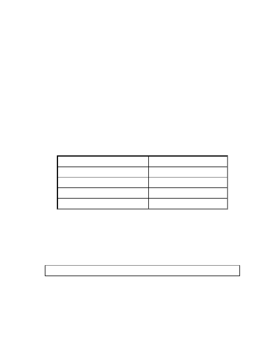
TABLE 2. ELECTRICAL TEST REQUIREMENTS
Mil-Std-883 Test Requirements
Subgroups
per Method 5005, Table 1
Interim Electric Parameters
Method 5004
1
Final Electrical Parameters
Method 5005
1*, 2, 3, 4
Group A Test Requirements
Method 5005
1, 2, 3, 4, 7, 8
Group C and D End-Point Electrical Parameters
Method 5005
1, 2*, 3*
* PDA applies to Subgroup 1 only.
** Guaranteed if not tested.
----------------------------
Electrical Characteristics of REF02 & 02A/883B
19-0346
Rev. C
for SMD 85514
Page 5 of
6