General Description
The MAXQ2000 microcontroller is a low-power, 16-bit
device that incorporates a liquid-crystal display (LCD)
interface that can drive up to 100 (-RBX) or 132 (-RAX)
segments. The MAXQ2000 is uniquely suited for the
blood-glucose monitoring market, but can be used in
any application that requires high performance and low-
power operation. The device can operate at a maximum
of either 14MHz (V
DD
> 1.8V) or 20MHz (V
DD
> 2.25V).
The MAXQ2000 has 32kWords of flash memory, 1kWord
of RAM, three 16-bit timers, and one or two universal
synchronous/asynchronous receiver/transmitters
(UARTs). Flash memory aids prototyping and low-vol-
ume production. The microcontroller core is powered by
a 1.8V supply, with a separate I/O supply for optimum
flexibility. An ultra-low-power sleep mode makes these
parts ideal for battery-powered, portable equipment.
Applications
Medical Instrumentation
Battery-Powered and Portable Devices
Electrochemical and Optical Sensors
Industrial Control
Data-Acquisition Systems and Data Loggers
Home Appliances
Consumer Electronics
Thermostats/Humidity Sensors
Security Sensors
Gas and Chemical Sensors
HVAC
Smart Transmitters
Features
High-Performance, Low-Power, 16-Bit RISC Core
DC to 20MHz Operation, Approaching 1MIPS per MHz
Dual 1.8V Core/3V I/O Enables Low Power/Flexible
Interfacing
33 Instructions, Most Single Cycle
Three Independent Data Pointers Accelerate Data
Movement with Automatic Increment/Decrement
16-Level Hardware Stack
16-Bit Instruction Word, 16-Bit Data Bus
16 x 16-Bit, General-Purpose Working Registers
Optimized for C-Complier (High-Speed/Density Code)
Program and Data Memory
32kWords Flash Memory, Mask ROM for High-
Volume Applications
10,000 Flash Write/Erase Cycles
1kWord of Internal Data RAM
JTAG/Serial Boot Loader for Programming
Peripheral Features
Up to 50 General-Purpose I/O Pins
100/132 Segment LCD Driver
Up to 4 COM and 36 Segments
Static, 1/2, and 1/3 LCD Bias Supported
No External Resistors Required
SPI
TM
and 1-Wire
�
(-RAX Only) Hardware I/O Ports
One or Two Serial UARTs
One-Cycle, 16 x 16 Hardware Multiply/Accumulate
with 48-Bit Accumulator
Three 16-Bit Programmable Timers/Counters
8-Bit, Subsecond, System Timer/Alarm
32-Bit, Binary Real-Time Clock with Time-of-Day Alarm
Programmable Watchdog Timer
Flexible Programming Interface
Bootloader Simplifies Programming
In-System Programming Through JTAG
Supports In-Application Programming of Flash Memory
Ultra-Low Power Consumption
190�A typ at 8MHz Flash Operation, PMM1 at 2.2V
700nA typ in Lowest Power Stop Mode
Low-Power 32kHz Mode and Divide-by-256 Mode
MAXQ2000
Low-Power LCD Microcontroller
______________________________________________ Maxim Integrated Products
1
Rev 2; 12/04
For pricing, delivery, and ordering information, please contact Maxim/Dallas Direct! at
1-888-629-4642, or visit Maxim's website at www.maxim-ic.com.
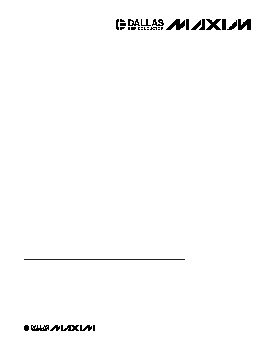
Ordering Information
Typical Operating Circuit and Pin Configurations appear at
end of data sheet.
PART
TEMP RANGE
PROGRAM
MEMORY
DATA
MEMORY
LCD
SEGMENTS
EXTERNAL
INTERRUPTS
UARTS
PIN-
PACKAGE
MAXQ2000-RAX
-40�C to +85�C
32kWord Flash
1kWord SRAM
132
16
2
68 QFN
MAXQ2000-RBX
-40�C to +85�C
32kWord Flash
1kWord SRAM
100
14
1
56 TQFN
Note: Some revisions of this device may incorporate deviations from published specifications known as errata. Multiple revisions of
any device may be simultaneously available through various sales channels. For information about device errata, go to:
www.maxim-ic.com/errata
.
MAXQ is a trademark of Maxim Integrated Products, Inc.
SPI is a trademark of Motorola, Inc.
1-Wire is a registered trademark of Dallas Semiconductor Corp.

MAXQ2000
Low-Power LCD Microcontroller
2
_____________________________________________________________________
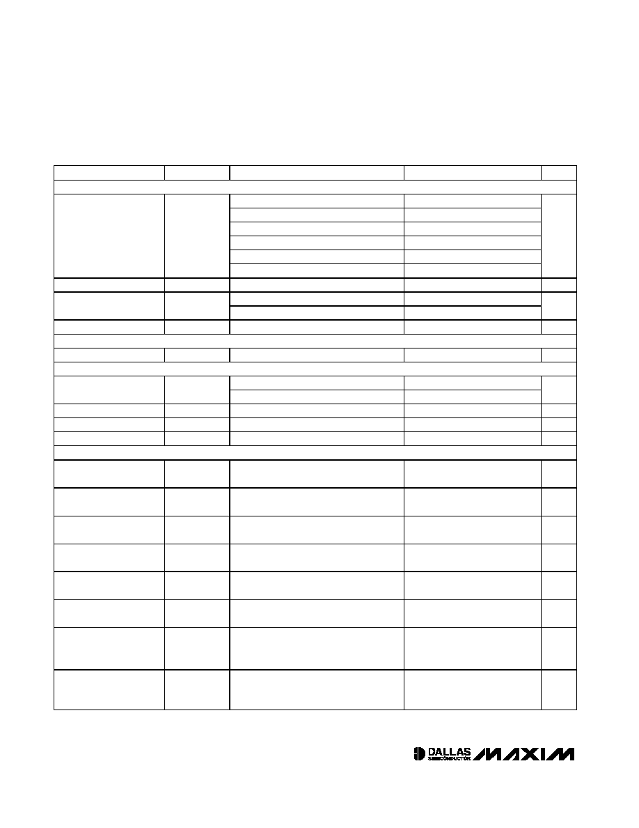
ABSOLUTE MAXIMUM RATINGS
ELECTRICAL CHARACTERISTICS
(V
DD
= V
DD(MIN)
to V
DD(MAX)
, V
DDIO
= 2.7V to 3.6V, T
A
= -40�C to +85�C.) (Note 1)
Stresses beyond those listed under "Absolute Maximum Ratings" may cause permanent damage to the device. These are stress ratings only, and functional
operation of the device at these or any other conditions beyond those indicated in the operational sections of the specifications is not implied. Exposure to
absolute maximum rating conditions for extended periods may affect device reliability.
Voltage Range on Any Pin Relative to
Ground Except V
DD .................................
-0.5V to (V
DDIO
+ 0.5)V
Voltage Range on V
DD
Relative to Ground .........-0.5V to +2.75V
Voltage Range on V
DDIO
Relative to Ground ........-0.5V to +3.6V
Operating Temperature Range ...........................-40�C to +85�C
Storage Temperature Range .............................-65�C to +150�C
Soldering Temperature ....................See IPC/JEDEC J-STD-020
.................................................................................
Specification
PARAMETER
SYMBOL
CONDITIONS
MIN
TYP
MAX
UNITS
32k x 16 flash
1.8
2.5
2.75
Core Supply Voltage
V
DD
Flash programming
2.25
2.5
2.75
V
I/O Supply Voltage
V
DDIO
V
DD
3.6
V
I
DD1
/1 mode
6.0
9.2
I
DD2
/2 mode
5.6
8.6
I
DD3
/4 mode
3.4
5.1
I
DD4
/8 mode
1.9
2.9
I
DD5
PMM1 mode
0.5
0.7
Active Current,
f
HFIN
= 14MHz
(Note 2)
I
DD6
PMM2 mode; 32KIN = 32.768kHz
4.8
7.6
mA
I
DD1
/1 mode
6.5
10.4
I
DD2
/2 mode
5.9
9.6
I
DD3
/4 mode
3.8
6.2
I
DD4
/8 mode
2.2
3.8
I
DD5
PMM1 mode
0.6
1.4
Active Current,
f
HFIN
= 20MHz
(Note 2)
I
DD6
PMM2 mode; 32KIN = 32.768kHz
4.8
8.1
mA
Execution from flash memory, 20MHz,
V
DD
= 2.2V, T
A
= +25�C
5.1
Execution from flash memory, 8MHz,
/8 mode, V
DD
= 2.2V, T
A
= +25�C
0.85
Execution from flash memory, 8MHz,
PMM1 mode, V
DD
= 2.2V, T
A
= +25�C
0.19
Execution from RAM, 8MHz,
/8 mode, V
DD
= 2.2V, T
A
= +25�C
0.30
Active Current
Execution from RAM, 1MHz,
/1 mode, V
DD
= 2.2V, T
A
= +25�C
0.14
mA
-40�C < T
A
< +25�C
0.7
55
Stop-Mode Current
I
STOP(VDD)
T
A
= +85�C
20
550
�A
Digital I/O Supply Current
I
DDIO
RTC enabled; HFIN 14MHz;
all I/O disconnected
1
50
�A
Input High Voltage:
HFIN and 32KIN
V
IH1
0.75 x
V
DDIO
V
DDIO
V

MAXQ2000
Low-Power LCD Microcontroller
_____________________________________________________________________
3
ELECTRICAL CHARACTERISTICS (continued)
(V
DD
= V
DD(MIN)
to V
DD(MAX)
, V
DDIO
= 2.7V to 3.6V, T
A
= -40�C to +85�C.) (Note 1)
PARAMETER
SYMBOL
CONDITIONS
MIN
TYP
MAX
UNITS
Input High Voltage:
P6.4�P6.5 and P7.0�P7.1
V
IH2
SVS on, V
LCD
= 3.3V
0.75 x
V
DDIO
V
LCD
V
Input High Voltage:
All Other Pins
V
IH3
0.75 x
V
DDIO
V
DDIO
V
Input Low Voltage:
HFIN and 32KIN
V
IL1
0
0.2 x
V
DDIO
V
Input Low Voltage:
All Other Pins
V
IL2
0
0.25 x
V
DDIO
V
Output High Voltage:
P6.4�P6.5 and P7.0�P7.1
V
OH1
SVS on; I
OH(MAX)
= 0.75mA; V
LCD
= 2.7V
V
LCD
-
0.2
V
Output High Voltage:
All Other Pins
V
OH2
I
OH(MAX)
= 0.75mA; V
DDIO
=1.8V
V
DDIO
-
0.2
V
Output Low Voltage for
All Other Pins
V
OL1
I
OL
= 1.0mA; V
DDIO
= 1.8V
GND
0.2
V
Output Low Voltage for
P6.4�P6.5 and P7.0�P7.1
V
OL2
I
OL
= 1.4mA; V
DDIO
= 2.7V
GND
0.2
V
Input Leakage Current
I
L
Internal pullup disabled
-100
+100
nA
Input Pullup Current
I
IP
Internal pullup enabled
-20
-5
�A
LCD INTERFACE
LCD Reference Voltage
V
LCD
2.7
3.3
3.6
V
LCD Bias Voltage 1
V
LCD1
1/3 bias
V
ADJ
+ 2/3 (V
LCD
- V
ADJ
)
V
LCD Bias Voltage 2
V
LCD2
1/3 bias
V
ADJ
+ 1/3 (V
LCD
- V
ADJ
)
V
LCD Adjustment Voltage
V
ADJ
Guaranteed by design
0
0.4 x
V
LCD Bias Resistor
R
LCD
100
k
LCD Adjustment Resistor
R
LADJ
LRA4:LRA0 = 0
200
k
When segment is driven at V
LCD
level;
V
LCD
= 3V; I
SEGxx
= -3�A;
guaranteed by design
V
LCD
-
0.02
V
LCD
When segment is driven at V
LCD1
level;
V
LCD1
= 2V; I
SEGxx
= -3�A;
guaranteed by design
V
LCD1
-
0.02
V
LCD1
When segment is driven at V
LCD2
level;
V
LCD2
= 1V; I
SEGxx
= -3�A;
guaranteed by design
V
LCD2
-
0.02
V
LCD2
LCD Segment Voltage
V
SEGxx
When segment is driven at V
ADJ
level;
V
ADJ
= 0V; I
SEGxx
= -3�A;
guaranteed by design
-0.1
V
ADJ
V
MAXQ2000
Low-Power LCD Microcontroller
4
_____________________________________________________________________
ELECTRICAL CHARACTERISTICS (continued)
(V
DD
= V
DD(MIN)
to V
DD(MAX)
, V
DDIO
= 2.7V to 3.6V, T
A
= -40�C to +85�C.) (Note 1)
PARAMETER
SYMBOL
CONDITIONS
MIN
TYP
MAX
UNITS
EXTERNAL CLOCK SOURCE
External oscillator, V
DD
2.25V
0
20
External oscillator, V
DD
< 2.25V
0
14
External crystal, V
DD
2.25V
3
20
External crystal, V
DD
< 2.25V
3
14
Flash programming, V
DD
2.25V
2
20
External-Clock Frequency
f
HFIN
Flash programming, V
DD
< 2.25V
2
14
MHz
External-Clock Period
t
CLCL
48% minimum duty cycle
50
ns
2.25V
V
DD
2.75V
0
20
System-Clock Frequency
f
CK
1.8V
V
DD
2.75V
0
14
MHz
System-Clock Period
t
CK
50
ns
REAL-TIME CLOCK
RTC Input Frequency
f
32KIN
32kHz watch crystal
32.768
kHz
JTAG/FLASH PROGRAMMING
Mass erase
200
Flash Erase Time
Page erase
20
ms
Flash Programming Time
2.5
5.0
ms
Write/Erase Cycles
10,000
cycles
Data Retention
100
years
SPI TIMING
SPI Master Operating
Frequency
1/t
MCK
f
CK
/ 2
MHz
SPI Slave Operating
Frequency
1/t
SCK
f
CK
/ 8
MHz
SCLK Output Pulse-Width
High/Low
t
MCH
, t
MCL
t
MCK
/ 2
- 25
ns
SCLK Input Pulse-Width
High/Low
t
SCH
, t
SCL
t
SCK
/ 2
ns
MOSI Output Hold Time
after SCLK Sample Edge
t
MOH
C
L
= 50pF
t
MCK
/ 2
- 25
ns
MOSI Output Valid to
Sample Edge
t
MOV
t
MCK
/ 2
- 25
ns
MISO Input Valid to SCLK
Sample Edge Rise/Fall
Setup
t
MIS
30
ns
MISO Input to SCLK
Sample Edge Rise/Fall
Hold
t
MIH
0
ns

MAXQ2000
Low-Power LCD Microcontroller
_____________________________________________________________________
5
Note 1: Specifications to -40�C are guaranteed by design and not production tested.
Note 2: Measured on the V
DD
pin with V
DD
= 2.75V and not in reset.
ELECTRICAL CHARACTERISTICS (continued)
(V
DD
= V
DD(MIN)
to V
DD(MAX)
, V
DDIO
= 2.7V to 3.6V, T
A
= -40�C to +85�C.) (Note 1)
PARAMETER
SYMBOL
CONDITIONS
MIN
TYP
MAX
UNITS
SCLK Inactive to MOSI
Inactive
t
MLH
t
MCK
/ 2
- 25
ns
MOSI Input to SCLK
Sample Edge Rise/Fall
Setup
t
SIS
30
ns
MOSI Input from SCLK
Sample Edge Transition
Hold
t
SIH
t
CK
+ 25
ns
MISO Output Valid after
SCLK Shift Edge
Transition
t
SOV
3t
CK
+ 25
ns
SSEL Inactive
t
SSH
t
CK
+ 25
ns
SCLK Inactive to
SSEL
Rising
t
SD
t
CK
+ 25
ns
MISO Output Disabled
after
CS Edge Rise
t
SLH
2t
CK
+ 50
ns