General Description
The MAX9205/MAX9207 serializers transform 10-bit-
wide parallel LVCMOS/LVTTL data into a serial high-
speed bus low-voltage differential signaling (LVDS)
data stream. The serializers typically pair with deserial-
izers like the MAX9206*/MAX9208*, which receive the
serial output and transform it back to 10-bit-wide paral-
lel data.
The MAX9205/MAX9207 transmit serial data at speeds
up to 400Mbps and 660Mbps, respectively, over PC
board traces or twisted-pair cables. Since the clock is
recovered from the serial data stream, clock-to-data
and data-to-data skew that would be present with a
parallel bus are eliminated.
The serializers require no external components and few
control signals. The input data strobe edge is selected
by TCLK_R/F. PWRDN is used to save power when the
devices are not in use. Upon power-up, a synchroniza-
tion mode is activated, which is controlled by two SYNC
inputs, SYNC1 and SYNC2.
The MAX9205 can lock to a 16MHz to 40MHz system
clock, while the MAX9207 can lock to a 40MHz to
66MHz system clock. The serializer output is held in
high impedance until the device is fully locked to the
local system clock, or when the device is in power-
down mode.
Both the devices operate from a single +3.3V supply,
are specified for operation from -40░C to +85░C, and
are available in 28-pin SSOP packages.
Applications
Features
o Standalone Serializer (vs. SERDES) Ideal for
Unidirectional Links
o Framing Bits for Deserializer Resync Allow Hot
Insertion Without System Interruption
o LVDS Serial Output Rated for Point-to-Point and
Bus Applications
o Wide Reference Clock Input Range
16MHz to 40MHz (MAX9205)
40MHz to 66MHz (MAX9207)
o Low 140ps (pk-pk) Deterministic Jitter (MAX9207)
o Low 34mA Supply Current (MAX9205)
o 10-Bit Parallel LVCMOS/LVTTL Interface
o Up to 660Mbps Payload Data Rate (MAX9207)
o Programmable Active Edge on Input Latch
o Pin-Compatible Upgrades to DS92LV1021 and
DS92LV1023
MAX9205/MAX9207
10-Bit Bus LVDS Serializers
________________________________________________________________ Maxim Integrated Products
1
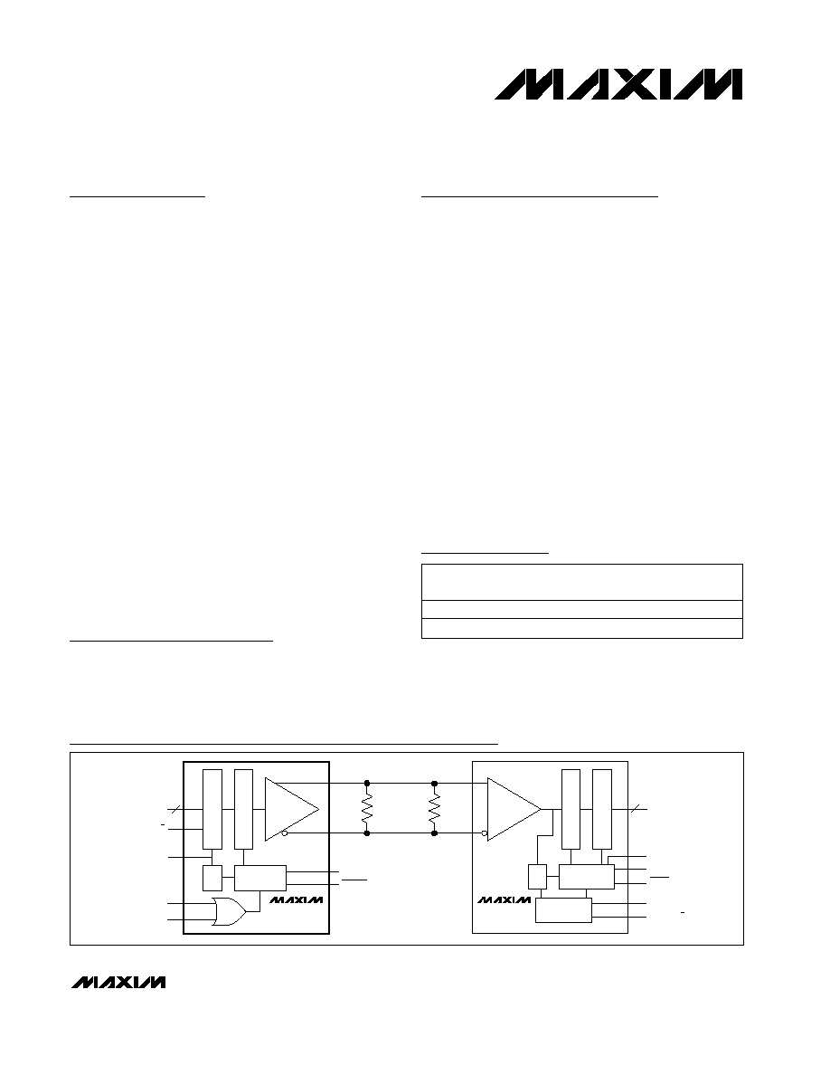
PC BOARD OR
TWISTED PAIR
TCLK
PLL
PLL
EN
EN
PWRDN
INPUT LATCH
PARALLEL-TO-SERIAL
OUTPUT LATCH
SERIAL-TO-PARALLEL
TIMING AND
CONTROL
TIMING AND
CONTROL
CLOCK
RECOVERY
RCLK
*FUTURE PRODUCT
LOCK
SYNC 1
SYNC 2
OUT+
OUT-
IN+
IN-
100
100
TCLK_R/F
RCLK_R/F
REFCLK
OUT_
IN_
10
10
BUS
LVDS
MAX9205
MAX9207
MAX9206*
MAX9208*
Ordering Information
19-2029; Rev 0; 5/01
For pricing, delivery, and ordering information, please contact Maxim/Dallas Direct! at
1-888-629-4642, or visit Maxim's website at www.maxim-ic.com.
PART
TEMP.
RANGE
PIN-
PACKAGE
REF CLOCK
RANGE (MHz)
M A X9 2 0 5 E AI
-40
░C to +85░C
28 SSOP
16 to 40
M A X9 2 0 7 E AI
-40
░C to +85░C
28 SSOP
40 to 66
Pin Configuration and Functional Diagram appear at end of
data sheet.
Typical Application Circuit
Cellular Phone Base
Stations
Add Drop Muxes
Digital Cross-Connects
DSLAMs
Network Switches and
Routers
Backplane Interconnect
*Future product¡contact factory for availability.

MAX9205/MAX9207
10-Bit Bus LVDS Serializers
2
_______________________________________________________________________________________
ABSOLUTE MAXIMUM RATINGS
DC ELECTRICAL CHARACTERISTICS
(V
CC
= +3.0V to +3.6V, R
L
= 27
▒1% or 50 ▒1%, C
L
= 10pF, T
A
= -40░C to +85░C. Typical values are at V
CC
= +3.3V and T
A
=
+25░C, unless otherwise noted.) (Notes 1, 2, 3)
Stresses beyond those listed under "Absolute Maximum Ratings" may cause permanent damage to the device. These are stress ratings only, and functional
operation of the device at these or any other conditions beyond those indicated in the operational sections of the specifications is not implied. Exposure to
absolute maximum rating conditions for extended periods may affect device reliability.
V
CC
to GND ........................................................-0.3V to +4.0V
IN_, SYNC1, SYNC2, EN, TCLK_R/F, TCLK,
PWRDN to GND......................................-0.3V to (V
CC
+ 0.3V)
OUT+, OUT- to GND .............................................-0.3V to +4.0V
Output Short-Circuit Duration.....................................Continuous
Continuous Power Dissipation (T
A
= +70░C)
28-Pin SSOP (derate 9.5mW/░C above +70░C) ..........762mW
Storage Temperature Range .............................-65░C to +150░C
Junction Temperature ......................................................+150░C
Operating Temperature Range ...........................-40░C to +85░C
Lead Temperature (soldering, 10s) .................................+300░C
ESD Protection (Human Body Model, OUT+, OUT-) ...........▒8kV
PARAMETER
SYMBOL
CONDITIONS
MIN
TYP
MAX
UNITS
LVCMOS/LVTLL LOGIC INPUTS (IN0 TO IN9, EN, SYNC1, SYNC2, TCLK, TCLK_R/F, PWRDN)
High-Level Input Voltage
V
IH
2.0
V
CC
V
Low-Level Input Voltage
V
IL
GND
0.8
V
Input Current
I
IN
V
IN_
= 0 or V
CC
-20
+20
ÁA
BUS LVDS OUTPUTS (OUT+, OUT-)
R
L
= 27
200
286
400
mV
Differential Output Voltage
V
OD
Figure 1
R
L
= 50
250
460
600
mV
Change in V
OD
Between
Complementary Output States
V
OD
Figure 1
1
35
mV
Output Offset Voltage
V
OS
Figure 1
0.9
1.15
1.3
V
Change in V
OS
Between
Complementary Output States
V
OS
Figure 1
3
35
mV
Output Short-Circuit Current
I
OS
OUT+ or OUT- = 0,
IN0 to IN9 = PWRDN = EN = high
-13
-15
mA
Output High-Impedance Current
I
OZ
PWRDN or EN = 0.8V,
OUT+ or OUT- = 0 or V
CC
-10
+10
ÁA
Power-Off Output Current
I
OX
V
CC
= 0, OUT+ or OUT- = 0 or 3.6V
-10
+10
ÁA
POWER SUPPLY
16MHz
23
35
MAX9205
40MHz
34
45
40MHz
32
50
Supply Current
I
CC
R
L
= 27
or 50
worst-case pattern
(Figures 2, 4)
MAX9207
66MHz
45
60
mA
Power-Down Supply Current
I
CCX
PWRDN = low
8
mA

MAX9205/MAX9207
10-Bit Bus LVDS Serializers
_______________________________________________________________________________________
3
AC ELECTRICAL CHARACTERISTICS
(V
CC
= +3.0V to +3.6V, R
L
= 27
▒1% or 50 ▒1%, C
L
= 10pF, T
A
= -40░C to +85░C. Typical values are at V
CC
= +3.3V and T
A
=
+25░C, unless otherwise noted.) (Notes 2, 4)
PARAMETER
SYMBOL
CONDITIONS
MIN
TYP
MAX
UNITS
TRANSMIT CLOCK (TCLK) TIMING REQUIREMENTS
MAX9205
16
40
MHz
TCLK Center Frequency
f
TCCF
MAX9207
40
66
MHz
TCLK Frequency Variation
TCFV
-200
200
ppm
MAX9205
25
62.5
TCLK Period
t
TCP
MAX9207
15.15
25
ns
TCLK Duty Cycle
TCDC
40
60
%
TCLK Input Transition Time
t
CLKT
Figure 3
3
6
ns
TCLK Input Jitter
t
JIT
150
ps
(RMS)
SWITCHING CHARACTERISTICS
R
L
= 27
150
300
400
Low-to-High Transition Time
t
LHT
Figure 4
R
L
= 50
150
350
500
ps
R
L
= 27
150
300
400
High-to-Low Transition Time
t
HLT
Figure 4
R
L
= 50
150
350
500
ps
IN_ Setup to TCLK
t
S
Figure 5
1
ns
IN_ Hold from TCLK
t
H
Figure 5
3
ns
OUTPUT High State to High-
Impedance Delay
t
HZ
Figures 6, 7
4.5
10
ns
OUTPUT Low State to High-
Impedance Delay
t
LZ
Figures 6, 7
4.5
10
ns
OUTPUT High Impedance to
High-State Delay
t
ZH
Figures 6, 7
4.5
10
ns
OUTPUT High Impedance to
Low-State Delay
t
ZL
Figures 6, 7
4.5
10
ns
SYNC Pulse Width
t
SPW
6 x t
TCP
ns
PLL Lock Time
t
PL
Figure 7
2048 x
t
TCP
2049 x
t
TCP
ns
Bus LVDS Bit Width
t
BIT
t
TCP
/ 12
ns
Serializer Delay
t
SD
Figure 8
t
TCP
/ 6
( t
TC P
/ 6)
+ 5
ns

MAX9205/MAX9207
10-Bit Bus LVDS Serializers
4
_______________________________________________________________________________________
Typical Operating Characteristics
(V
CC
= +3.3V, R
L
= 27
, C
L
= 10pF, T
A
= +25░C, unless otherwise noted.)
10
30
20
40
50
3.0
3.3
3.6
WORST-CASE PATTERN SUPPLY CURRENT
vs. SUPPLY VOLTAGE
MAX9205 toc01
SUPPLY VOLTAGE (V)
SUPPLY CURRENT (mA)
TCLK = 40MHz
MAX9205
10
50
20
60
3.0
3.6
DETERMINISTIC JITTER vs.
SUPPLY VOLTAGE
MAX9205 toc02
SUPPLY VOLTAGE (V)
DETERMINISTIC JITTER (ps, pk-pk)
3.3
40
30
TCLK = 40MHz
MAX9205
AC ELECTRICAL CHARACTERISTICS (continued)
(V
CC
= +3.0V to +3.6V, R
L
= 27
▒1% or 50 ▒1%, C
L
= 10pF, T
A
= -40░C to +85░C. Typical values are at V
CC
= +3.3V and T
A
=
+25░C, unless otherwise noted.) (Notes 2, 4)
Note 1: Current into a pin is defined as positive. Current out of a pin is defined as negative. All voltages are referenced to ground
except V
OD
,
V
OD
, and V
OS
.
Note 2: C
L
includes scope probe and test jig capacitance.
Note 3: Parameters 100% tested at T
A
= +25░C. Limits over operating temperature range guaranteed by design and characterization.
Note 4: AC parameters are guaranteed by design and characterization.
PARAMETER
SYMBOL
CONDITIONS
MIN
TYP
MAX
UNITS
16MHz
200
MAX9205
40MHz
140
40MHz
140
Deterministic Jitter (Figure 9)
t
DJIT
MAX9207
66MHz
140
ps
(pk-pk)
16MHz
13
MAX9205
40MHz
9
40MHz
9
Random Jitter (Figure 10)
t
RJIT
MAX9207
66MHz
6
ps
(RMS)

MAX9205/MAX9207
10-Bit Bus LVDS Serializers
_______________________________________________________________________________________
5
Pin Description
PIN
NAME
FUNCTION
1, 2
SYNC 1,
SYNC 2
LVCMOS/LVTTL Logic Inputs. The two SYNC pins are ORed. When at least one of the two pins
are asserted high for at least six cycles of TCLK, the serializer initiates a transmission of 1024
SYNC patterns. If held high after 1024 SYNC patterns have been transmitted, SYNC patterns
continue to be sent until the SYNC pin is asserted low. Toggling a SYNC pin after six TCLK cycles
high and before 1024 SYNC patterns have been transmitted does not affect the output of the 1024
SYNC patterns.
3¡12
IN0¡IN9
LVCMOS/LVTTL Data Inputs. Data is loaded into a 10-bit latch by the selected TCLK edge.
13
TCLK_R/F
LVCMOS/LVTTL Logic Input. High selects a TCLK rising-edge data strobe. Low selects a TCLK
falling-edge data strobe.
14
TCLK
LVCMOS/LVTTL Reference Clock Input. The MAX9205 accepts a 16MHz to 40MHz clock. The
MAX9207 accepts a 40MHz to 66MHz clock. TCLK provides a frequency reference to the PLL and
strobes parallel data into the input latch.
15, 16
DGND
Digital Circuit Ground. Connect to ground plane.
17, 26
AV
CC
Analog Circuit Power Supply (Includes PLL). Bypass AV
CC
to ground with a 0.1
ÁF capacitor and a
0.001
ÁF capacitor. Place the 0.001ÁF capacitor closest to AV
CC
.
18, 20,
23, 25
AGND
Analog Circuit Ground. Connect to ground plane.
19
EN
LVCMOS/LVTTL Logic Input. High enables serial data output. Low puts the bus LVDS output into
high impedance.
21
OUT-
Inverting Bus LVDS Differential Output
22
OUT+
Noninverting Bus LVDS Differential Output
24
PWRDN
LVCMOS/LVTTL Logic Input. Low puts the device into power-down mode and the output into high
impedance.
27, 28
DV
CC
Digital Circuit Power Supply. Bypass DV
CC
to ground with a 0.1
ÁF capacitor and a 0.001ÁF
capacitor. Place the 0.001
ÁF capacitor closest to DV
CC
.
Detailed Description
The MAX9205/MAX9207 are 10-bit serializers designed
to transmit data over balanced media that may be a
standard twisted-pair cable or PC board traces at
160Mbps to 660Mbps. The interface may be double-
terminated point-to-point or a heavily loaded multipoint
bus. The characteristic impedance of the media and
connected devices can range from 100
for a point-to-
point interface to 54
for a heavily loaded multipoint
bus. A double-terminated point-to-point interface uses
a 100
-termination resistor at each end of the inter-
face, resulting in a load of 50
. A heavily loaded multi-
point bus requires a termination as low as 54
at each
end of the bus, resulting in a termination load of 27
.
The serializer requires a deserializer such as the
MAX9206/MAX9208 for a complete data transmission
application.
A high-state start bit and a low-state stop bit, added
internally, frame the 10-bit parallel input data and
ensure a transition in the serial data stream. Therefore,
12 serial bits are transmitted for each 10-bit parallel
input. The MAX9205 accepts a 16MHz to 40MHz refer-
ence clock, producing a serial data rate of 192Mbps
(12 bits x 16MHz) to 480Mbps (12 bits x 40MHz). The
MAX9207 accepts a 40MHz to 66MHz reference clock,
producing 480Mbps to 792Mbps. However, since only
10 bits are from input data, the actual throughput is 10
times the TCLK frequency.
To transmit data, the serializers sequence through
three modes: initialization mode, synchronization mode,
and data transmission mode.