Äîêóìåíòàöèÿ è îïèñàíèÿ www.docs.chipfind.ru
General Description
The MAX9125/MAX9126 quad low-voltage differential
signaling (LVDS) line receivers are ideal for applica-
tions requiring high data rates, low power, and reduced
noise. The MAX9125/MAX9126 are guaranteed to
receive data at speeds up to 500Mbps (250MHz) over
controlled-impedance media of approximately 100
.
The transmission media may be printed circuit (PC)
board traces or cables.
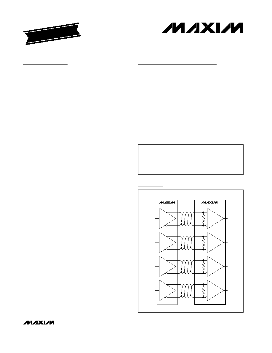
The MAX9125/MAX9126 accept four LVDS differential
inputs and translate them to 3.3V CMOS outputs. The
MAX9126 features integrated parallel termination resis-
tors (nominally 115
), which eliminate the requirement
for four discrete termination resistors and reduce stub
length. The MAX9125 inputs are high impedance and
require an external termination resistor when used in a
point-to-point connection.
The devices support a wide common-mode input range
of 0.05V to 2.35V, allowing for ground potential differ-
ences and common-mode noise between the driver
and the receiver. A fail-safe feature sets the output high
when the inputs are open, or when the inputs are
undriven and shorted or parallel terminated. The EN
and EN inputs control the high-impedance output and
are common to all four receivers. Inputs conform to the
ANSI TIA/EIA-644 LVDS standard. The MAX9125/
MAX9126 operate from a single +3.3V supply, are
specified for operation from -40°C to +85°C, and are
available in 16-pin TSSOP and SO packages. Refer to
the MAX9124 data sheet for a quad LVDS line driver.
Applications
Digital Copiers
Laser Printers
Cellular Phone Base Stations
Add/Drop Muxes
Digital Cross-Connects
DSLAMs
Network Switches/Routers
Backplane Interconnect
Clock Distribution
Features
o Integrated Termination Eliminates Four External
Resistors (MAX9126)
o Pin Compatible with DS90LV032A
o Guaranteed 500Mbps Data Rate
o 300ps Pulse Skew (max)
o Conform to ANSI TIA/EIA-644 LVDS Standard
o Single +3.3V Supply
o Low 70µA Shutdown Supply Current
o Fail-Safe Circuit
MAX9125/MAX9126
Quad LVDS Line Receivers with
Integrated Termination
________________________________________________________________ Maxim Integrated Products
1
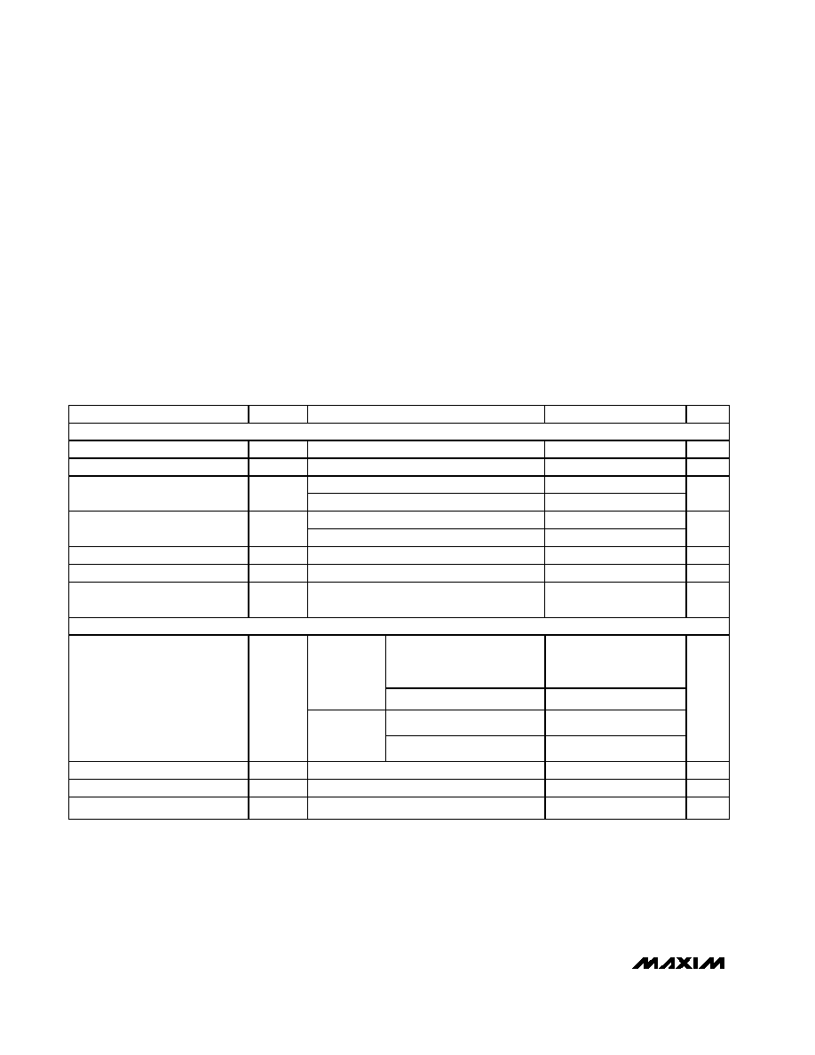
Ordering Information
115
MAX9124
MAX9126
115
115
115
R
X
LVDS SIGNALS
100
SHIELDED TWISTED CABLE OR MICROSTRIP PC BOARD TRACES
LVTTL/LVCMOS
DATA INPUT
LVTTL/LVCMOS
DATA OUTPUT
R
X
R
X
R
X
T
X
T
X
T
X
T
X
Typical Application Circuit
19-1908; Rev 0; 5/01
EVALUATION KIT
AVAILABLE
PART
TEMP. RANGE
PIN-PACKAGE
MAX9125EUE
-40°C to +85°C
16 TSSOP
MAX9125ESE
-40°C to +85°C
16 SO
MAX9126EUE
-40°C to +85°C
16 TSSOP
MAX9126ESE
-40°C to +85°C
16 SO
Pin Configuration appears at end of data sheet.
For pricing, delivery, and ordering information, please contact Maxim/Dallas Direct! at
1-888-629-4642, or visit Maxim's website at www.maxim-ic.com.
MAX9125/MAX9126
Quad LVDS Line Receivers with
Integrated Termination
2
_______________________________________________________________________________________
ABSOLUTE MAXIMUM RATINGS
DC ELECTRICAL CHARACTERISTICS
(V
CC
= +3.0V to +3.6V, differential input voltage
|
V
ID
|
= 0.1V to 1.0V, common-mode voltage V
CM
=
|
V
ID
/2
|
to 2.4V -
|
V
ID
/2
|
, T
A
=
-40°C to +85°C. Typical values are at V
CC
= +3.3V, T
A
= +25°C, unless otherwise noted.) (Note 1)
Stresses beyond those listed under "Absolute Maximum Ratings" may cause permanent damage to the device. These are stress ratings only, and functional
operation of the device at these or any other conditions beyond those indicated in the operational sections of the specifications is not implied. Exposure to
absolute maximum rating conditions for extended periods may affect device reliability.
V
CC
to GND ...........................................................-0.3V to +4.0V
IN_+, IN_- to GND .................................................-0.3V to +4.0V
EN, EN to GND ...........................................-0.3V to (V
CC
+ 0.3V)
OUT_ to GND .............................................-0.3V to (V
CC
+ 0.3V)
Continuous Power Dissipation (T
A
= +70°C)
16-Pin TSSOP (derate 9.4mW/°C above +70°C) .........755mW
16-Pin SO (derate 8.7mW/°C above +70°C)................696mW
Storage Temperature Range .............................-65°C to +150°C
Maximum Junction Temperature .....................................+150°C
Operating Temperature Range ...........................-40°C to +85°C
Lead Temperature (soldering, 10s) .................................+300°C
ESD Protection (Human Body Model) IN_+, IN_-, OUT_............±7.5kV
PARAMETER
SYMBOL
CONDITIONS
MIN
TYP
MAX
UNITS
LVDS INPUTS (IN_+, IN_-)
Differential Input High Threshold
V
TH
100
mV
Differential Input Low Threshold
V
TL
-100
mV
0.1V
V
ID
0.6V,
-20
20
Input Current (MAX9125)
I
IN
_+,
I
IN
_-
0.6V
<V
ID
1.0V
-25
25
µA
0.1V
V
ID
0.6V, V
CC
= 0
-20
20
Power-Off Input Current
(MAX9125)
I
IN
_+,
I
IN
_-
0.6V
<V
ID
1.0V, V
CC
= 0
-25
25
µA
Input Resistor 1
R
IN1
V
CC
= +3.6V or 0, Figure 1
35
k
Input Resistor 2
R
IN2
V
CC
= +3.6V or 0, Figure 1
132
k
Differential Input Resistance
(MAX9126)
R
DIFF
V
CC
= +3.6V or 0, Figure 1
90
115
132
LVCMOS/LVTTL OUTPUTS (OUT_)
Open, undriven short, or
undriven 100
parallel
termination
2.7
3.2
I
OH
=
-4.0mA
(MAX9125)
V
ID
= +100mV
2.7
3.2
Open or undriven short
2.7
3.2
Output High Voltage
V
OH
I
OH
=
-4.0mA
(MAX9126)
V
ID
= +100mV
2.7
3.2
V
Output Low Voltage
V
OL
I
OL
= +4.0mA, V
ID
= -100mV
0.1
0.25
V
Output Short-Circuit Current
I
OS
Enabled, V
ID
= +100mV, V
OUT
_ = 0 (Note 2)
-15
-120
mA
Output High-Impedance Current
I
OZ
Disabled, V
OUT
_ = 0 or V
CC
-10
+10
µA
MAX9125/MAX9126
Quad LVDS Line Receivers with
Integrated Termination
_______________________________________________________________________________________
3
DC ELECTRICAL CHARACTERISTICS (continued)
(V
CC
= +3.0V to +3.6V, differential input voltage
|
V
ID
|
= 0.1V to 1.0V, common-mode voltage V
CM
=
|
V
ID
/2
|
to 2.4V -
|
V
ID
/2
|
, T
A
=
-40°C to +85°C. Typical values are at V
CC
= +3.3V, T
A
= +25°C, unless otherwise noted.) (Note 1)
AC ELECTRICAL CHARACTERISTICS
(V
CC
= +3.0V to +3.6V, C
L
= 10pF, differential input voltage
|
V
ID
|
= 0.2V to 1.0V, common-mode voltage V
CM
=
|
V
ID
/2
|
to 2.4V
-
|
V
ID
/2
|
, input rise and fall time = 1ns (20% to 80%), input frequency = 100MHz, T
A
= -40°C to +85°C. Typical values are at V
CC
=
+3.3V, V
CM
= 1.2V,
|
V
ID
|
= 0.2V, T
A
= +25°C, unless otherwise noted.) (Notes 3, 4)
PARAMETER
SYMBOL
CONDITIONS
MIN
TYP
MAX
UNITS
LOGIC INPUTS (EN, EN)
Input High Voltage
V
IH
2.0
V
CC
V
Input Low Voltage
V
IL
0
0.8
V
Input Current
I
IN
V
IN
= V
CC
or 0
-15
15
µA
SUPPLY
Supply Current
I
CC
Enabled, inputs open
9
15
mA
Disabled Supply Current
I
CCZ
Disabled, inputs open
70
500
µA
PARAMETER
SYMBOL
CONDITIONS
MIN
TYP
MAX
UNITS
Differential Propagation Delay
High to Low
t
PHLD
Figures 2 and 3
1.8
2.4
3.3
ns
Differential Propagation Delay
Low to High
t
PLHD
Figures 2 and 3
1.8
2.3
3.3
ns
Differential Pulse Skew
[t
PHLD
-
t
PLHD
] (Note 5)
t
SKD1
Figures 2 and 3
100
300
ps
Differential Channel-to-Channel
Skew (Note 6)
t
SKD2
Figures 2 and 3
400
ps
Differential Part-to-Part Skew
(Note 7)
t
SKD3
Figures 2 and 3
0.8
ns
Differential Part-to-Part Skew
(Note 8)
t
SKD4
Figures 2 and 3
1.5
ns
Rise Time
t
TLH
Figures 2 and 3
0.34
1.2
ns
Fall Time
t
THL
Figures 2 and 3
0.32
1.2
ns
Disable Time High to Z
t
PHZ
R
L
= 2k
, Figures 4 and 5
12
ns
Disable Time Low to Z
t
PLZ
R
L
= 2k
, Figures 4 and 5
12
ns
Enable Time Z to High
t
PZH
R
L
= 2k
, Figures 4 and 5
17
ns
Enable Time Z to Low
t
PZL
R
L
= 2k
, Figures 4 and 5
17
ns
Maximum Operating Frequency
(Note 9)
f
MAX
All channels switching
250
300
MHz
2.2
2.4
2.3
2.6
2.5
2.7
2.8
100
900
1300
500
1700
2100
2500
DIFFERENTIAL PROPAGATION DELAY
vs. DIFFERENTIAL INPUT VOLTAGE
MAX9125/6 toc03
DIFFERENTIAL INPUT VOLTAGE (mV)
DIFFERENTIAL PROPAGATION DELAY (ns)
t
PHLD
t
PLHD
Typical Operating Characteristics
(V
CC
= +3.3V,
|
V
ID
|
= 200mV, V
CM
= +1.2V, C
L
= 10pF, frequency = 10MHz, T
A
= +25°C, unless otherwise noted.) (Figures 2 and 3)
MAX9125/MAX9126
Quad LVDS Line Receivers with
Integrated Termination
4
_______________________________________________________________________________________
Note 1: Current into a pin is defined as positive. Current out of a pin is defined as negative. All voltages are referenced to ground
except V
TH
, V
TL
, and V
ID
.
Note 2: Short only one output at a time. Do not exceed the absolute maximum junction temperature specification.
Note 3: AC parameters are guaranteed by design and characterization.
Note 4: C
L
includes scope probe and test jig capacitance.
Note 5: t
SKD1
is the magnitude difference of differential propagation delays in a channel; t
SKD1
=
|
t
PHLD
- t
PLHD
|
.
Note 6: t
SKD2
is the magnitude difference of the t
PLHD
or t
PHLD
of one channel and the t
PLHD
or t
PHLD
of any other channel on the
same part.
Note 7: t
SKD3
is the magnitude difference of any differential propagation delays between parts operating over rated conditions at
the same V
CC
and within 5°C of each other.
Note 8: t
SKD4
is the magnitude difference of any differential propagation delays between parts operating over rated conditions.
Note 9: f
MAX
generator output conditions: t
R
= t
F
< 1ns (0% to 100%), 50% duty cycle, V
OL
= 1.1V, V
OH
= 1.3V. Receiver output
criteria: 60% to 40% duty cycle, V
OL
= 0.4V (max), V
OH
= 2.7V (min), load = 10pF.
100
0
0.01
0.1
1
10
100
1000
SUPPLY CURRENT vs. SWITCHING
FREQUENCY, FOUR CHANNELS SWITCHING
20
MAX9125/6 toc01
SWITCHING FREQUENCY (MHz)
SUPPLY CURRENT (mA)
40
60
80
10
30
50
70
90
V
CC
= +3.6V
V
CC
= +3.3V
V
CC
= +3V
2.8
2.6
2.4
2.2
2.0
-40
10
-15
35
60
85
DIFFERENTIAL PROPAGATION DELAY
vs. TEMPERATURE
MAX9125/6 toc02
TEMPERATURE (
°C)
DIFFERENTIAL PROPAGATION DELAY (ns)
t
PHLD
t
PLHD
AC ELECTRICAL CHARACTERISTICS (continued)
(V
CC
= +3.0V to +3.6V, CL = 10pF, differential input voltage
|
V
ID
|
= 0.2V to 1.0V, common-mode voltage V
CM
=
|
V
ID
/2
|
to 2.4V
-
|
V
ID
/2
|
, input rise and fall time = 1ns (20% to 80%), input frequency = 100MHz, T
A
= -40°C to +85°C. Typical values are at V
CC
=
+3.3V, V
CM
= 1.2V,
|
V
ID
|
= 0.2V, T
A
= +25°C, unless otherwise noted.) (Notes 3, 4)
MAX9125/MAX9126
Quad LVDS Line Receivers with
Integrated Termination
_______________________________________________________________________________________
5
Typical Operating Characteristics (continued)
(V
CC
= +3.3V,
|
V
ID
|
= 200mV, V
CM
= +1.2V, C
L
= 10pF, frequency = 10MHz, T
A
= +25°C, unless otherwise noted (Figures 2 and 3).)
PIN
NAME
FUNCTION
1, 7, 9, 15
IN_-
Inverting Differential Receiver Inputs
2, 6, 10, 14
IN_+
Noninverting Differential Receiver Inputs
3, 5, 11, 13
OUT_
LVCMOS/LVTTL Receiver Outputs
4, 12
EN, EN
Receiver Enable Inputs. When EN = low and EN = high, the outputs are disabled and in high
impedance. For other combinations of EN and EN, the outputs are active.
8
GND
Ground
16
V
CC
Power Supply Input. Bypass V
CC
to GND with 0.1
µF and 0.001µF ceramic capacitors.
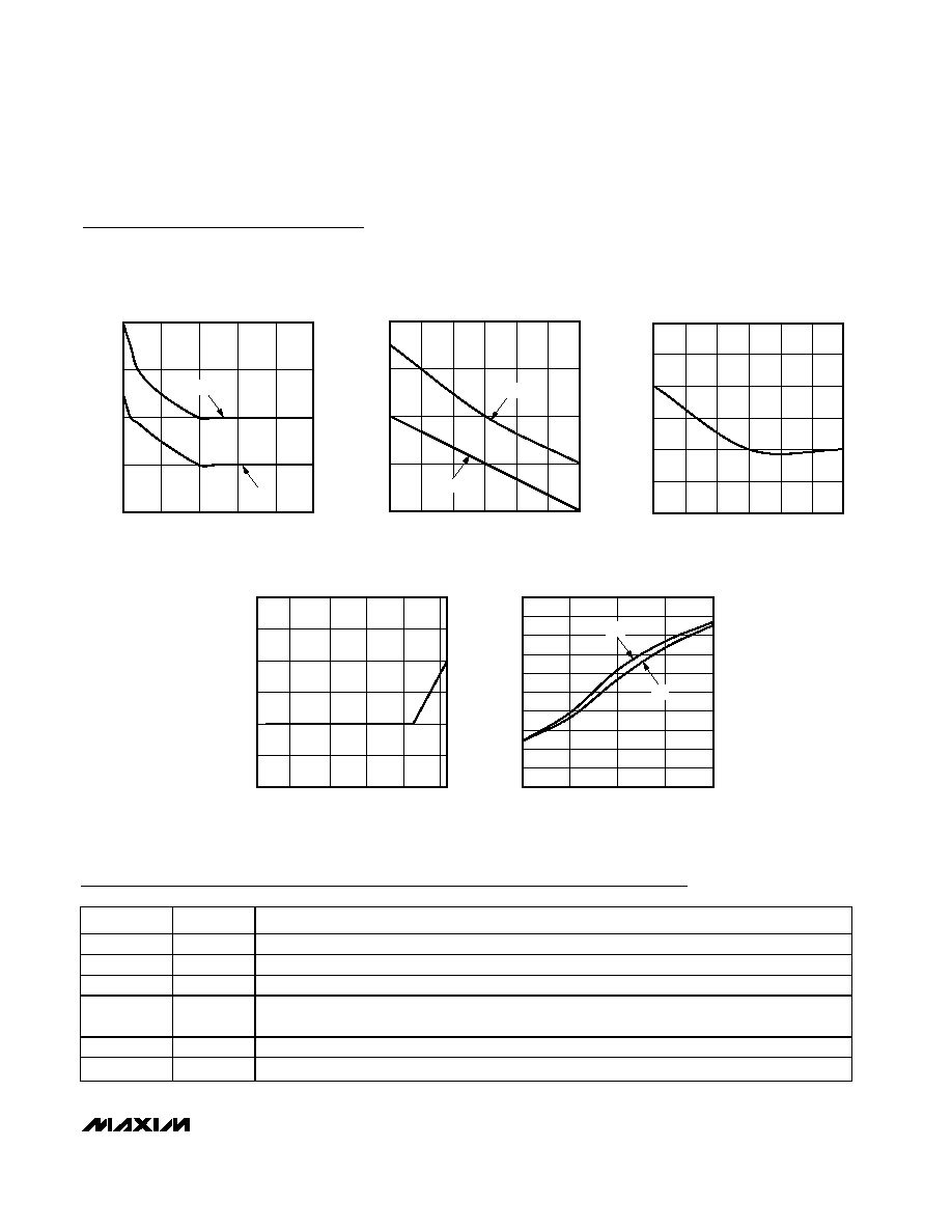
Pin Description
2.6
2.5
2.4
2.3
2.2
0
1.0
0.5
1.5
2.0
2.5
DIFFERENTIAL PROPAGATION DELAY
vs. COMMON-MODE VOLTAGE
MAX9125/6 toc04
COMMON-MODE VOLTAGE (V)
DIFFERENTIAL PROPAGATION DELAY (ns)
t
PHLD
t
PLHD
50
100
75
150
125
175
200
-40
10
35
-15
60
85
PULSE SKEW vs. TEMPERATURE
MAX9125/6 toc07
TEMPERATURE (
°C)
SKEW (ps)
0
900
400
200
500
1000
5
15
10
20
25
TRANSITION TIME vs. CAPACITIVE LOAD
MAX9125/6 toc08
CAPACITIVE LOAD (pF)
TRANSITION TIME (ps)
t
TLH
t
THL
800
700
600
300
100
2.2
2.3
2.5
2.4
2.6
3.0
3.2
3.3
3.1
3.4
3.5
3.6
DIFFERENTIAL PROPAGATION DELAY
vs. SUPPLY VOLTAGE
MAX9125/6 toc05
SUPPLY VOLTAGE (V)
DIFFERENTIAL PROPAGATION DELAY (ns)
t
PHLD
t
PLHD
50
100
75
150
125
175
200
3.0
3.2
3.3
3.1
3.4
3.5
3.6
PULSE SKEW vs. SUPPLY VOLTAGE
MAX9125/6 toc06
SUPPLY VOLTAGE (V)
SKEW (ps)