
General Description
The MAX8887/MAX8888 low-dropout linear regulators
operate from a 2.5V to 5.5V input and deliver up to
300mA continuous (500mA pulsed) current. The
MAX8887 is optimized for low-noise operation, while the
MAX8888 includes an open-drain POK ouput flag. Both
regulators feature exceptionally low 100mV dropout at
200mA. These devices are available in a variety of pre-
set output voltages in the 1.5V to 3.3V range.
An internal PMOS pass transistor allows the low 55µA
supply current to remain independent of load, making
these devices ideal for portable battery-powered equip-
ment such as personal digital assistants (PDAs), cellu-
lar phones, cordless phones, and notebook computers.
Other features include a micropower shutdown mode,
short-circuit protection, thermal shutdown protection,
and an active-low open-drain power-OK (POK) output
that indicates when the output is out of regulation. The
MAX8887/MAX8888 are available in a thin 5-pin SOT23
package that is only 1mm high.
________________________Applications
Notebook Computers
Wireless Handsets
PDAs and Palmtop Computers
Digital Cameras
PCMCIA Cards
Hand-Held Instruments
Features
Guaranteed 300mA Output Current (500mA for
Pulsed Loads)
Low 100mV Dropout at 200mA Load
POK Output (MAX8888)
42µV
RMS
Output Noise (MAX8887)
Preset Output Voltages (1.5V, 1.8V, 2.85V, and
3.3V)
55µA No-Load Supply Current
Thermal Overload and Short-Circuit Protection
Foldback Output Current-Limit Protection
60dB PSRR at 1kHz
0.1µA Shutdown Current
Thin 5-Pin SOT23 Package, 1mm High
MAX8887/MAX8888
Low-Dropout, 300mA Linear Regulators in SOT23
________________________________________________________________ Maxim Integrated Products
1
GND
BP
SHDN
1
5
OUT
IN
MAX8887
TOP VIEW
2
3
4
GND
POK
SHDN
1
5
OUT
IN
MAX8888
2
3
4
Pin Configurations
MAX8887
MAX8888
ON
OFF
INPUT
2.5V TO 5.5V
IN
SHDN
GND
(BP)
POK
OUT
V
OUT
300mA
C
IN
2.2
µF
C
OUT
2.2
µF
C
BP
0.01
µF
( ) ARE FOR MAX8887 ONLY.
Typical Operating Circuit
19-1859; Rev 2; 6/04
Ordering Information
PART
TEMP
RANGE
PIN-
PACKAGE
TOP
MARK
M A X8 8 8 7
E Z K15- T
-40
°C to +85°C 5 SOT23-5
ADQD
MAX8887EZK18- T
-40
°C to +85°C 5 SOT23-5
ADPX
MAX8887EZK29- T
-40
°C to +85°C 5 SOT23-5
ADPY
MAX8887EZK33- T
-40
°C to +85°C 5 SOT23-5
ADPZ
MAX8887EZKxy- T*
-40
°C to +85°C 5 SOT23-5
--
M A X8 8 8 8
E Z K15- T
-40
°C to +85°C 5 SOT23-5
ADQE
MAX8888EZK18- T
-40
°C to +85°C 5 SOT23-5
ADQA
MAX8888EZK29- T
-40
°C to +85°C 5 SOT23-5
ADQB
MAX8888EZK33- T
-40
°C to +85°C 5 SOT23-5
ADQC
MAX8888EZKxy- T*
-40
°C to +85°C 5 SOT23-5
--
*Other versions (xy) between +1.5 and +3.3V are available in
100mV increments. Contact factory for other versions. Minimum
order quantity is 25,000 units.
For pricing, delivery, and ordering information, please contact Maxim/Dallas Direct! at
1-888-629-4642, or visit Maxim's website at www.maxim-ic.com.
MAX8887/MAX8888
Low-Dropout, 300mA Linear Regulators in SOT23
2
_______________________________________________________________________________________
ABSOLUTE MAXIMUM RATINGS
ELECTRICAL CHARACTERISTICS
(V
IN
= V
OUT
+ 1V,
SHDN = IN, T
A
= -40°C to +85°C, unless otherwise noted.) (Note 1)
Stresses beyond those listed under "Absolute Maximum Ratings" may cause permanent damage to the device. These are stress ratings only, and functional
operation of the device at these or any other conditions beyond those indicated in the operational sections of the specifications is not implied. Exposure to
absolute maximum rating conditions for extended periods may affect device reliability.
IN, SHDN, POK, to GND...........................................-0.3V to +7V
OUT, BP to GND ............................................-0.3 to (V
IN
+ 0.3V)
Output Short-Circuit Duration.....................................Continuous
Continuous Power Dissipation (T
A
= +70
°C)
5-Pin SOT23 (derate 9.1mW/
°C above +70°C)............727mW
Operating Temperature Ranges..........................-40
°C to +85°C
Junction Temperature ......................................................+150
°C
Storage Temperature Range .............................-65
°C to +150°C
Lead Temperature (soldering, 10s) .................................+500
°C
PARAMETER
SYMBOL
CONDITIONS
MIN
TYP
MAX
UNITS
Input Voltage
V
IN
2.5
5.5
V
Input Undervoltage Lockout
V
IN
rising
(2% typical hysteresis)
2.15
2.4
V
T
A
= +25°C, I
OUT
= 100mA
-1.2
+1.2
I
OUT
= 100µA to 300mA,
T
A
= 0
°C to +85°C
-2
+2
Output Voltage Accuracy
I
OUT
= 100µA to 300mA
-3
+3
%
Continuous
300
Maximum Output Current
10ms pulse
500
mA
V
OUT
= 0
300
Current Limit
V
OUT
> 93% of nominal value
420
mA
No load
55
100
Ground-Pin Current
I
OUT
= 300mA
65
µA
I
OUT
= 1mA
0.5
I
OUT
= 200mA
100
200
Dropout Voltage (Note 2)
V
OUT
= +3.3V
I
OUT
= 300mA
150
mV
Line Regulation
V
IN
= 2.5V or (V
OUT
+ 0.4V) to 5.5V,
I
OUT
= 5mA
-0.15
0
0.15
%/V
MAX8887
10Hz to 100kHz, C
BP
= 0.01µF,
C
OUT
= 2.2µF, ESR
COUT
< 0.1
42
Output Noise
MAX8888
10Hz to 100kHz, C
OUT
= 2.2µF,
ESR
COUT
< 0.1
360
µV
RMS
MAX8887
f < 1kHz, C
BP
= 0.01µF,
C
OUT
= 4.7µF, ESR
COUT
< 0.1
60
PSRR
MAX8888
f < 1kHz, C
OUT
= 2.2µF,
ESR
COUT
< 0.1
40
dB
MAX8887/MAX8888
Low-Dropout, 300mA Linear Regulators in SOT23
_______________________________________________________________________________________
3
PARAMETER
SYMBOL
CONDITIONS
MIN
TYP
MAX
UNITS
SHUTDOWN
Shutdown Supply Current
SHDN = GND, V
IN
= 5.5V
0.1
2
µA
V
IH
2.5V
V
IN
5.5V
1.6
SHDN Input Threshold
V
IL
2.5V
V
IN
5.5V
0.6
V
SHDN Input Bias Current
SHDN = IN or GND
10
100
nA
OUT Discharge Resistance in
Shutdown
SHDN = GND
650
1100
POK (MAX8888 ONLY)
POK Trip Level, Referred to OUT
Set Point
V
OUT
falling
(1% typical hysteresis)
90
92.5
95
%
Operating IN Voltage Range for
Valid POK
1.0
5.5
V
POK Output Voltage Low
V
OL
I
SINK
= 1mA
0.1
V
POK Output Leakage Current
V
POK
= 5.5V, SHDN = IN
100
nA
THERMAL PROTECTION
Thermal Shutdown Temperature
170
°C
Thermal Shutdown Hysteresis
20
°C
ELECTRICAL CHARACTERISTICS (continued)
(V
IN
= V
OUT
+ 1V, SHDN = IN, T
A
= -40°C to +85°C, unless otherwise noted.) (Note 1)
Note 1:
All parts are 100% tested at T
A
= +25°C. Limits over the operating temperature range are guaranteed by design.
Note 2:
Typical and maximum dropout voltage for different output voltages are shown in the Typical Operating Characteristics
curve.
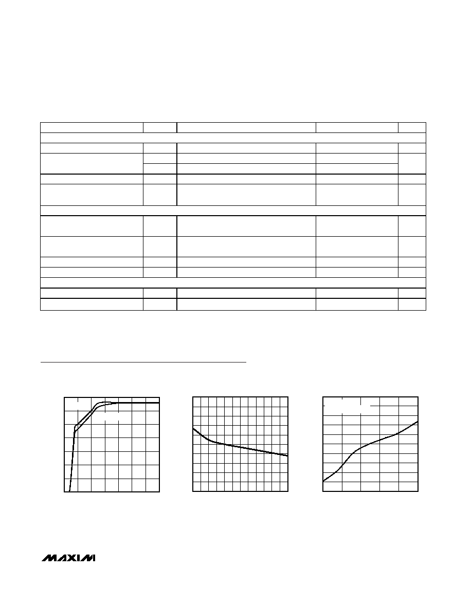
Typical Operating Characteristics
(Typical Operating Circuit, T
A
= +25°C, unless otherwise noted.)
0
1.0
0.5
2.0
1.5
3.0
2.5
3.5
2.0
3.0
3.5
2.5
4.0
4.5
5.0
5.5
OUTPUT VOLTAGE vs. INPUT VOLTAGE
MAX8887/8 toc01
INPUT VOLTAGE (V)
OUTPUT VOLTAGE (V)
I
OUT
= 0
I
OUT
= 300mA
-1.0
-0.6
-0.8
0.0
-0.2
-0.4
0.2
0.4
0.8
0.6
1.0
100
50
150
200
250
300
OUTPUT VOLTAGE ACCURACY
vs. LOAD CURRENT
MAX8887/8 toc02
LOAD CURRENT (mA)
% DEVIATION (%)
0
-0.05
-0.02
-0.03
-0.04
-0.01
0.0
0.01
0.02
0.03
0.04
0.05
-40
10
-15
35
60
85
OUTPUT VOLTAGE ACCURACY
vs. TEMPERATURE
MAX8887/8 toc03
TEMPERATURE (
°C)
% DEVIATION
I
OUT
= 0
V
IN
= V
OUT
+ 500mV
MAX8887/MAX8888
Low-Dropout, 300mA Linear Regulators in SOT23
4
_______________________________________________________________________________________
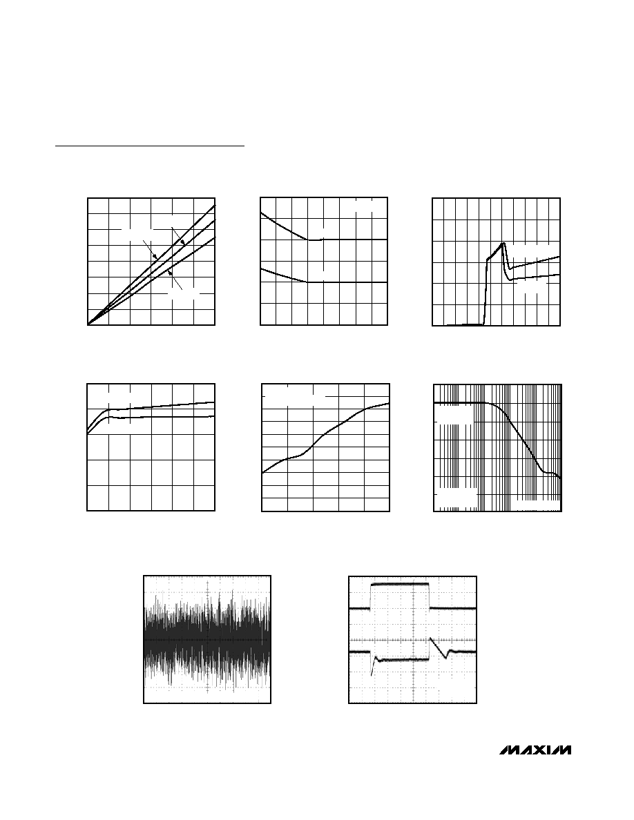
0
20
40
60
80
100
120
140
160
0
100
50
150
200
250
300
DROPOUT VOLTAGE vs. LOAD CURRENT
MAX8887/8 toc04
LOAD CURRENT (mA)
V
DROPOUT
(mV)
T
A
= +25
°C
T
A
= +85
°C
T
A
= -40
°C
0
50
100
150
200
250
300
2.5
2.7
2.9
3.1
3.3
DROPOUT VOLTAGE vs. OUTPUT VOLTAGE
MAX8887/8 toc05
V
OUT
(V)
V
DROPOUT
(mV)
I
OUT
= 200mA
MAXIMUM
TYPICAL
0
1.0
2.0
3.0
4.0
5.0
INPUT VOLTAGE (V)
0
50
25
100
75
125
150
GROUND-PIN CURRENT vs. INPUT VOLTAGE
MAX8887/8 toc06
GROUND-PIN CURRENT (
µ
A)
I
LOAD
= 300mA
I
LOAD
= 0
0
20
60
40
80
100
0
100
50
150
200
250
300
GROUND-PIN CURRENT vs. LOAD CURRENT
MAX8887/8 toc07
LOAD CURRENT (mA)
GROUND-PIN CURRENT (
µ
A)
V
IN
= 5.5V
V
IN
= 3.8V
50
56
54
52
58
60
62
64
66
68
70
-40
10
-15
35
60
85
GROUND-PIN CURRENT vs. TEMPERATURE
MAX8887/8 toc08
TEMPERATURE (
°C)
GROUND-PIN CURRENT (
µ
A)
I
OUT
= 0
V
IN
= V
OUT
+ 500mV
70
0.01
0.1
1
10
100
1000
60
50
40
30
20
POWER-SUPPLY REJECTION RATIO
vs. FREQUENCY
MAX8887/8 toc09
FREQUENCY (kHz)
PSRR (dB)
10
0
C
OUT
= 2.2
µF
C
BP
= 0.01
µF
V
OUT
= 3.30V
I
LOAD
= 30mA
MAX8887 ONLY
MAX8887
OUTPUT NOISE DC TO 1MHz
V
OUT
50
µV/div
MAX8887/8 toc10
40ms/div
V
OUT
= 1.8V, V
IN
= 3.8V, I
LOAD
= 15mA
LOAD-TRANSIENT RESPONSE
50mV/div
AC-COUPLED
MAX8887/8 toc11
300mA
10mA
V
OUT
I
OUT
V
OUT
= 3.3V
V
IN
= 3.8V
10
µs/div
Typical Operating Characteristics (continued)
(Typical Operating Circuit, T
A
= +25°C, unless otherwise noted.)

MAX8887/MAX8888
Low-Dropout, 300mA Linear Regulators in SOT23
_______________________________________________________________________________________
5
LINE-TRANSIENT RESPONSE
MAX8887/8 toc13
20mV/div
AC-COUPLED
4V
4.5V
V
OUT
V
IN
V
OUT
= 3.3V
I
LOAD
= 100mA
100
µs/div
SHUTDOWN WAVEFORM
MAX8887/8 toc14
V
SHDN
1V/div
DC-COUPLED
2V/div
V
OUT
V
OUT
= 3.3V, R
LOAD
= 10
20
µs/div
POK WAVEFORM
MAX8887/8 toc15
2V/div
2V/div
2V/div
V
OUT
V
POK
V
IN
V
OUT
= 3.3V, R
LOAD
= 100
20ms/div
Pin Description
MAX8887
MAX8888
NAME
FUNCTION
1
1
IN
Regulator Input. Supply voltage can range from 2.5V to 5.5V. Bypass with 2.2µF
capacitor to GND (see the Capacitor Selection and Regulator Stability section).
2
2
GND
Ground
3
3
SHDN
Active-Low Shutdown Input. A logic low reduces the supply current to below 0.1µA.
In shutdown, POK and OUT are driven low. Connect to IN for normal operation.
--
4
POK
Open-Drain Active-Low POK Output. POK remains low while the output voltage (V
OUT
) is
below the reset threshold. Connect a 100k
pullup resistor to OUT to obtain a logic level
output. POK is driven low in shutdown. If not used, leave this pin unconnected.
4
--
BP
Reference Bypass. Bypass with a low-leakage 0.01µF ceramic capacitor.
5
5
OUT
Regulator Output. Sources up to 300mA guaranteed. Bypass with 2.2µF (<0.2
typical
ESR) ceramic capacitor to GND.
LOAD-TRANSIENT RESPONSE
NEAR DROPOUT
MAX8887/8 toc12
50mV/div
AC-COUPLED
300mA
10mA
V
OUT
I
OUT
V
OUT
= 3.3V
V
IN
= 3.4V
10
µs/div
Typical Operating Characteristics (continued)
(Typical Operating Circuit, T
A
= +25°C, unless otherwise noted.)