General Description
The MAX8737 dual high-power linear regulator con-
trollers use external n-channel MOSFETs to generate
two independent low-voltage supplies for notebook
computers. The MAX8737 delivers low output voltages
from 0.5V to 2.5V (±5mV no-load accuracy). The exter-
nal components allow scalable current design with
loads up to 5A with excellent load regulation (1%). The
regulator operates from a low input voltage, which also
reduces the power dissipation in the external n-channel
MOSFET. The controller powers the external MOSFET
gate driver from the standard 5V system supply.
The MAX8737 includes current and thermal limits to
prevent damage to the linear regulator. The MAX8737
uses an external resistive divider to fold back the cur-
rent limit, reducing the overall power dissipation. The
MAX8737 uses an external resistive-divider in series
with the current-sense input (CS_), providing foldback
current-limit protection, and effectively reducing the
short-circuit power dissipation.
An output undervoltage timeout is available for low-cost
applications that omit the current-sense resistor. The
output undervoltage (UVP) timing depends on the mag-
nitude of the voltage at V
OUT
. The UVP detects and
shuts down the LDO if the output voltage drops out of
regulation. The controller uses an adjustable reference
input (REFIN_) to set the nominal output voltage
(V
OUT_
), which minimizes the cost and makes the sta-
bility independent of the output voltage.
Each linear regulator features an adjustable soft-start
function, and generates a delayed power-good
(PGOOD) signal that signals when the linear regulator
is in regulation. The MAX8737 is a low-cost solution
requiring few external components and is available in a
small, 4mm x 4mm, 16-pin thin QFN package.
Applications
Notebook and Desktop Computers
Point-of-Load Regulators
V
MCH
and V
CCP
CPU Supplies
Low-Voltage Bias Supplies
Servers
Features
Low-Cost Dual Linear Regulators
Output Voltage Accuracy ±5mV
Independent 0.5V to 2.5V Reference Inputs
Foldback Current-Limit Protection
Output Undervoltage-Lockout Protection
Thermal Limit (Internal Sensor)
1.0V to 5.5V Input Supply Voltage (External FET
Drain)
5V Bias Supply Voltage
Independent Power-Good Open-Drain Outputs
Independent Enable Inputs
Soft-Shutdown Output Discharge
Low Supply Current (0.5mA)
5µA (max) Shutdown Supply Current
MAX8737
Dual, Low-Voltage Linear Regulator Controllers
with External MOSFETs
________________________________________________________________ Maxim Integrated Products
1
16
1
2
3
4
12
11
10
9
15
14
13
5
6
7
8
DRV1
GND
N.C.
DRV2
N.C.
CS2
OUT2
REFIN2
CS1
OUT1
REFIN1
PGOOD2
PGOOD1
EN2
EN1
V
CC
TOP VIEW
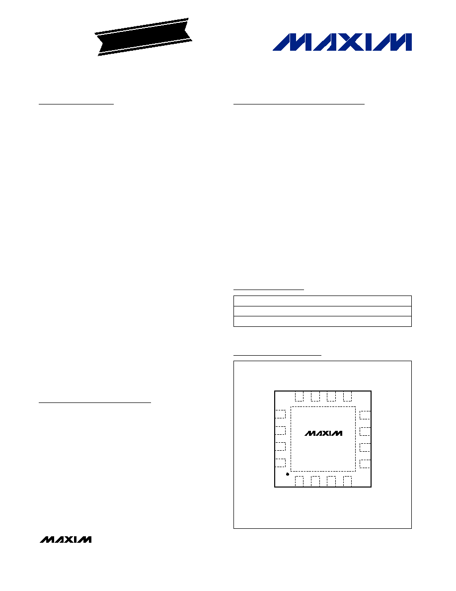
MAX8737
4mm x 4mm TQFN
Pin Configuration
19-3705; Rev 0; 5/05
For pricing, delivery, and ordering information, please contact Maxim/Dallas Direct! at
1-888-629-4642, or visit Maxim's website at www.maxim-ic.com.
EVALUATION KIT
AVAILABLE
Ordering Information
PART
TEMP RANGE PIN-PACKAGE
MAX8737ETE
-40°C to +85°C 16 Thin QFN-EP* 4mm x 4mm
MAX8737ETE+ -40°C to +85°C 16 Thin QFN-EP* 4mm x 4mm
*EP = Exposed pad.
+Denotes lead-free packaging.
MAX8737
Dual, Low-Voltage Linear Regulator Controllers
with External MOSFETs
2
_______________________________________________________________________________________
ABSOLUTE MAXIMUM RATINGS
Stresses beyond those listed under "Absolute Maximum Ratings" may cause permanent damage to the device. These are stress ratings only, and functional
operation of the device at these or any other conditions beyond those indicated in the operational sections of the specifications is not implied. Exposure to
absolute maximum rating conditions for extended periods may affect device reliability.
V
CC
to GND ..............................................................-0.3V to +6V
OUT1, OUT2 to GND................................................-0.3V to +6V
REFIN1, REFIN2, PGOOD1, PGOOD2, EN1,
EN2 to GND..........................................................-0.3V to +6V
DRV1, DRV2, CS1, CS2 to GND.................-0.3V to (V
CC
+ 0.3V)
Continuous Power Dissipation (T
A
= +70°C)
16-Pin 4mm x 4mm Thin QFN (derated 25mW/°C
above +70°C).............................................................2000mW
Operating Temperature Range
MAX8737ETE ...................................................-40°C to +85°C
Junction Temperature ......................................................+150°C
Storage Temperature Range .............................-65°C to +150°C
Lead Temperature (soldering, 10s) .................................+300°C
ELECTRICAL CHARACTERISTICS
(V
CC
= 5V, EN_ = CS_ = V
CC
, V
REFIN
= 1.0V, T
A
= 0°C to +85°C, unless otherwise noted. Typical values are at T
A
= +25°C.)
PARAMETER
SYMBOL
CONDITIONS
MIN
TYP
MAX
UNITS
Supply Voltage Range
V
CC
4.75
5.50
V
V
CC
Undervoltage Lockout
Threshold
Rising edge, 200mV hysteresis (typ)
4.1
4.35
4.6
V
V
CC
Quiescent Supply Current
I
CC
EN1 = EN2 = V
CC
0.5
1
mA
V
CC
Shutdown Supply Current
EN1 = EN2 = GND
0.1
5
µA
REFIN to OUT Offset Voltage
V
OUT
_
-5
+5
mV
OUT_ Input Bias Current
I
OUT
_
-1
+1
µA
DRIVERS
Output high; V
OUT
_ = V
REFIN
_ - 25mV,
I
LOAD
= 1mA
V
CC
-
0.3
V
CC
-
0.05
DRV_ Output Voltage Swing
(Note 1)
Output low; V
OUT
_ = V
REFIN
_ + 25mV,
I
LOAD
= 1mA
0.03
0.3
V
DRV_ Maximum Sourcing Current
V
OUT
_ = V
REFIN
_ - 25mV; V
DRV
= 3V
6
14
mA
DRV_ Maximum Sinking Current
V
OUT
_ = V
REFIN
_ + 25mV; V
DRV
= 3V
6
14
mA
OUT_ to DRV_ Transconductance
(Large Signal)
G
MDRV
0.8
S
DRV_ Power-Supply Rejection
Ratio
10Hz < f < 10kHz, I
DRV
= 1mA, C
DRV
=
10nF
-80
dB
DRV_ Soft-Start Charging Current
I
SOFT
40
170
400
µA
REFERENCE INPUT
REFIN_ Voltage Range
V
REFIN
_
V
CC
= 4.75V to 5.5V
0.5
2.5
V
REFIN_ Input Bias Current
I
REFIN
_
V
REFIN
_ = 0 to 2.5V
-100
-10
+100
nA
FAULT PROTECTION
Thermal Shutdown Threshold
T
SHDN
Hysteresis = 20°C
+125
°C
T
A
= 0°C to +85°C
7
10
13
Current-Limit Threshold
V
ILIM
V
CS
_ - V
OUT
_
T
A
= +85°C
7.5
10
12.5
mV
CS_ Input Current
-1
+1
µA
Linear Regulator UVP Threshold
(Slow)
UVP
(SLOW)
With respect to V
REFIN
; CS_ = V
CC
72
80
88
%
MAX8737
Dual, Low-Voltage Linear Regulator Controllers
with External MOSFETs
_______________________________________________________________________________________
3
ELECTRICAL CHARACTERISTICS (continued)
(V
CC
= 5V, EN_ = CS_ = V
CC
, V
REFIN
= 1.0V, T
A
= 0°C to +85°C, unless otherwise noted. Typical values are at T
A
= +25°C.)
PARAMETER
SYMBOL
CONDITIONS
MIN
TYP
MAX
UNITS
Linear Regulator UVP Threshold
(Fast)
UVP
(FAST)
With respect to V
REFIN
; CS_ = V
CC
54
60
66
%
Slow Short-Circuit Timer Duration
t
UVP(SLOW)
With respect to V
REFIN
; CS_ = V
CC
75
µs
Fast Short-Circuit Timer Duration
t
UVP(FAST)
With respect to V
REFIN
; CS_ = V
CC
5
µs
Discharge-Mode On-Resistance
OUT_ Pin
R
OUT
10
INPUTS AND OUTPUTS
EN_ Input Low Level
0.6
V
EN_ Input High Level
Rising edge, 200mV (typ) hysteresis
1.6
V
Enable Leakage Current
-1
+1
µA
Power-Good Trip Threshold
(Lower)
With respect to error comparator threshold,
hysteresis = 4% (falling edge)
-15
-12
-9
%
Power-Good Startup Delay
2
ms
Power-Good Propagation Delay
t
PGOOD
OUT_ forced 2% beyond PGOOD_ trip
threshold
1
µs
Power-Good Output Low Voltage
I
SINK
= 4mA
0.3
V
Power Good Leakage Current
I
GOO
V
OUT
_ = 1.0V (PGOOD_ high impedance),
1
µA
ELECTRICAL CHARACTERISTICS
(V
CC
= 5V, EN_ = CS_ = V
CC
, V
REFIN
= 1.0V, T
A
= -40°C to +85°C, unless otherwise noted.) (Note 2)
PARAMETER
SYMBOL
CONDITIONS
MIN
TYP
MAX
UNITS
Supply Voltage Range
V
CC
4.75
5.50
V
V
CC
Undervoltage Lockout
Threshold
Rising edge 200mV hysteresis (typ)
4.1
4.6
V
V
CC
Quiescent Supply Current
I
CC
EN1 = EN2 = V
CC
1.5
mA
V
CC
Shutdown Supply Current
EN1 = EN2 = GND
5
µA
REFIN to OUT Offset Voltage
V
OUT
_
-7
+7
mV
DRIVERS
Output high; V
OUT
_ = V
REFIN
_ - 25mV;
I
LOAD
= 1mA
V
CC
-
0.3
DRV_ Output Voltage Swing
(Note 1)
Output low; V
OUT
_ = V
REFIN
_ + 25mV:
I
LOAD
= 1mA
0.3
V
DRV_ Maximum Sourcing Current
V
OUT
_ = V
REFIN
_ - 25mV; V
DRV
= 3V
3.5
mA
DRV_ Maximum Sinking Current
V
OUT
_ = V
REFIN
_ + 25mV; V
DRV
= 3V
3.5
mA
DRV_ Soft-Start Charging Current
I
SOFT
40
400
µA
MAX8737
Dual, Low-Voltage Linear Regulator Controllers
with External MOSFETs
4
_______________________________________________________________________________________
ELECTRICAL CHARACTERISTICS (continued)
(V
CC
= 5V, EN_ = CS_ = V
CC
, V
REFIN
= 1.0V, T
A
= -40°C to +85°C, unless otherwise noted.) (Note 2)
PARAMETER
SYMBOL
CONDITIONS
MIN
TYP
MAX
UNITS
REFERENCE INPUT
REFIN_ Voltage Range
V
REFIN
_
V
CC
= 4.75V to 5.5V
0.5
2.5
V
FAULT PROTECTION
Current-Limit Threshold
V
ILIM
V
CS
_ - V
OUT
_
6.5
13.5
mV
Linear Regulator UVP Threshold
(Slow)
UVP
(SLOW)
With respect to V
REFIN
; CS_ = V
CC
72
88
%
Linear Regulator UVP Threshold
(Fast)
UVP
(FAST)
With respect to V
REFIN
; CS_ = V
CC
54
66
%
INPUTS AND OUTPUTS
EN_ Input Low Level
0.6
V
EN_ Input High Level
1.6
V
Power-Good Trip Threshold
(Lower)
With respect to error comparator threshold,
hysteresis = 4% (falling edge)
-15
-9
%
Power-Good Output Low Voltage
I
SINK
= 4mA
0.3
V
Note 1: Low threshold n-channel MOSFET is required for 2.5V (±2%) output.
Note 2: Specifications to -40°C are guaranteed by design, not production tested.
Typical Operating Characteristics
(Circuit of Figure 1, T
A
= +25°C, unless otherwise noted.)
OUTPUT-VOLTAGE DEVIATION
vs. LOAD CURRENT
MAX8737 toc01
LOAD CURRENT (A)
OUTPUT-VOLTAGE DEVIATION (mV)
1.5
1.0
0.5
-4
-3
-2
-1
0
1
2
3
4
5
-5
0
2.0
V
OUT
= 1.5V
FOLDBACK CURRENT LIMIT
vs. OUTPUT VOLTAGE
MAX8737 toc02
OUTPUT VOLTAGE (V)
CURRENT LIMIT (A)
1.0
0.5
0.4
0.8
1.2
1.6
2.0
2.4
2.8
3.2
0
0
1.5
1ms/div
SOFT-START
(EN RISING EDGE)
5V
3V
C
A
D
MAX8737 toc03
0
0
0
0
1.5V
5V
A. EN1, 5V/div
B. DRV1, 2V/div
NO LOAD
C. LDO1 OUTPUT, 1V/div
D. PGOOD1, 5V/div
B

MAX8737
Dual, Low-Voltage Linear Regulator Controllers
with External MOSFETs
_______________________________________________________________________________________
5
100
µs/div
SOFT-STOP
(EN FALLING EDGE)
5V
3V
C
A
D
MAX8737 toc04
0
0
0
0
1.5V
5V
A. EN1, 5V/div
B. DRV1, 2V/div
NO LOAD
C. LDO1 OUTPUT, 1V/div
D. PGOOD1, 5V/div
B
2ms/div
SOFT-START
(UVLO RISING EDGE)
5V
3V
C
A
D
MAX8737 toc05
0
0
0
0
1.5V
5V
A. 5V BIAS (V
CC
), 5V/div
B. DRV1, 2V/div
NO LOAD, EN = V
CC
C. LDO1 OUTPUT, 1V/div
D. PGOOD1, 5V/div
B
2ms/div
SOFT-STOP
(UVLO FALLING EDGE)
5V
3V
C
A
D
MAX8737 toc06
0
0
0
0
1.5V
5V
A. 5V BIAS (V
CC
), 5V/div
B. DRV1, 2V/div
NO LOAD, EN = V
CC
C. LDO1 OUTPUT, 1V/div
D. PGOOD1, 5V/div
B
10
µs/div
LOAD TRANSIENT
(0.1A TO 2.1A)
0
0.1A
C
A
D
MAX8737 toc07
1.50V
1.49V
2.1A
3.2V
2.8V
A. CONTROL SIGNAL
B. LOAD CURRENT, 2A/div
C. DRV1, 500mV/div
D. LDO1 OUTPUT VOLTAGE,
10mV/div
B
1.51V
10
µs/div
LOAD TRANSIENT
(NO LOAD TO 2A)
0
0
C
A
D
MAX8737 toc08
1.50V
1.45V
2A
3.2V
2.7V
A. CONTROL SIGNAL
B. LOAD CURRENT, 2A/div
C. DRV1, 1V/div
D. LDO1 OUTPUT VOLTAGE,
50mV/div
B
1.7V
2
µs/div
LOAD TRANSIENT
(NO LOAD TO 2A)
0
0
C
A
D
MAX8737 toc09
1.50V
1.45V
2A
3.2V
2.7V
A. CONTROL SIGNAL
B. LOAD CURRENT, 2A/div
C. DRV1, 1V/div
D. LDO1 OUTPUT VOLTAGE,
50mV/div
B
Typical Operating Characteristics (continued)
(Circuit of Figure 1, T
A
= +25°C, unless otherwise noted.)

MAX8737
Dual, Low-Voltage Linear Regulator Controllers
with External MOSFETs
6
_______________________________________________________________________________________
DRV TRANSCONDUCTANCE
DISTRIBUTION
MAX8737 toc13
TRANSCONDUCTANCE (S)
SAMPLE PERCENTAGE (%)
1.3
1.0
0.8
10
20
30
40
50
0
0.5
1.5
SAMPLE SIZE = 150
OUT1
OUT2
OUTPUT-VOLTAGE DEVIATION
vs. TEMPERATURE
MAX8737 toc14
TEMPERATURE (
°C)
OUTPUT-VOLTAGE DEVIATION (mV)
60
35
10
-15
-2
-1
0
1
2
3
-3
-40
85
0.1
1
10
0.001
0.01
GAIN AND PHASE
(OUT1)
60
MAX8737 toc15
20
0
GAIN (dB)
PHASE (
°
)
40
-20
180
0
-90
90
-180
FREQUENCY (MHz)
1.5V OUTPUT, 1A LOAD, C
OUT
= (1) 10
µF 1206 16V CERAMIC
0.1
1
10
0.001
0.01
GAIN AND PHASE
(OUT2)
60
MAX8737 toc16
20
0
GAIN (dB)
PHASE (
°
)
40
-20
180
0
-90
90
-180
FREQUENCY (MHz)
1.05V OUTPUT, 2A LOAD, C
OUT
= (1) 22
µF 1206 6V CERAMIC
Typical Operating Characteristics (continued)
(Circuit of Figure 1, T
A
= +25°C, unless otherwise noted.)
2
µs/div
FOLDBACK CURRENT LIMIT
(SHORT-CIRCUIT RESPONSE)
10V
C
A
D
MAX8737 toc10
1.50V
5V
3V
20A
0
A. GATE OF FET LOAD, 10V/div
B. DRV1, 1V/div
C. MOSFET CURRENT, 20A/div
D. LD01 OUTPUT
VOLTAGE, 2V/div
E. PGOOD1, 5V/div
B
0
0
0
1.5V
E
OUTPUT OFFSET VOLTAGE
DISTRIBUTION
MAX8737 toc11
OUTPUT OFFSET VOLTAGE (mV)
SAMPLE PERCENTAGE (%)
3
0
-3
10
20
30
40
50
0
-5
5
SAMPLE SIZE = 150
OUT1
OUT2
CURRENT-LIMIT THRESHOLD
DISTRIBUTION
MAX8737 toc12
CURRENT LIMIT (mV)
SAMPLE PERCENTAGE (%)
11.3
10.0
8.8
10
20
30
40
50
0
7.5
12.5
SAMPLE SIZE = 150
OUT1
OUT2

MAX8737
Dual, Low-Voltage Linear Regulator Controllers
with External MOSFETs
_______________________________________________________________________________________
7
MAX8737
Dual, Low-Voltage Linear Regulator Controllers
with External MOSFETs
Pin Description
PIN
NAME
FUNCTION
1
V
CC
Analog and Driver Supply Input. Connect to the system supply voltage (+5.0V). Bypass V
CC
to analog
ground with a 1µF or greater ceramic capacitor.
2
CS1
Positive Current-Sense Input for LDO1. To enable (foldback) current limit, connect CS1 to the positive
terminal of the current-sense element as shown in Figure 1. The MAX8737 driver reduces the gate
voltage when the 10mV (typ) current-limit threshold is exceeded. When CS1 is connected to V
CC
, the
MAX8737 disables the current-limit protection and enables the output undervoltage protection (see the
UVP Short-Circuit Protection section).
3
OUT1
Outp ut Feed b ack- S ense, N eg ati ve C ur r ent- S ense, and D i schar g e Inp ut for LD O 1. C onnect d i r ectl y to the
l i near r eg ul ator outp ut. W hen LD O1 i s d i sab l ed , OU T1 i s d i schar g ed thr oug h an i nter nal 10
FE T to GN D .
4
REFIN1
External Reference Input for LDO1. REFIN1 sets the main output regulation voltage (V
OUT1
= V
REFIN1
).
5
PGOOD2
Open-Drain Power-Good Output for LDO2. PGOOD2 is low when the output voltage is more than 12%
(typ) below the normal regulation point, during soft-start, and in shutdown. Approximately 2ms (typ) after
OUT2 reaches the regulation voltage (REFIN2), PGOOD2 becomes high impedance as long as the
output remains in regulation.
6
PGOOD1
Open-Drain Power-Good Output for LDO1. PGOOD1 is low when the output voltage is more than 12%
(typ) below the normal regulation point, during soft-start, and in shutdown. Approximately 2ms (typ) after
OUT1 reaches the regulation voltage (REFIN1), PGOOD1 becomes high impedance as long as the
output remains in regulation.
7
EN2
Enable Input for LDO2. Connect EN2 to Vcc for always ON. When EN2 is pulled low, the linear regulator
shuts down and pulls the output to ground.
8
EN1
Enable Input for LDO1. Connect EN1 to Vcc for always ON. When EN1 is pulled low, the linear regulator
shuts down and pulls the output to ground.
9
REFIN2
External Reference Input for the Secondary Regulator (LDO2). REFIN2 sets the main output regulation
voltage (V
OUT2
= V
REFIN2
).
10
OUT2
Output Sense, Negative Current-Sense Input, and Discharge Input for the Secondary Regulator (LDO2).
Connect directly to the linear regulator output. When the LDO2 is disabled, OUT2 is discharged through
an internal 10
FET to GND.
11
CS2
Positive Current-Sense Input for LDO2. To enable (foldback) current limit, connect CS2 to the positive
terminal of the current-sense element as shown in Figure 1. The MAX8737 driver reduces the gate
voltage when the 10mV (typ) current-limit threshold is exceeded. When CS2 is connected to V
CC
, the
MAX8737 disables the current-limit protection and enables the output undervoltage protection (see the
UVP Short-Circuit Protection section).
12, 14
N.C.
Not Internally Connected
13
DRV2
External N-Channel Gate Drive for LDO2
15
GND
Ground. Connect the thin QFN backside pad to GND.
16
DRV1
External N-Channel Gate Drive for LDO1
--
EP
Exposed Pad. Connect the thin QFN backside pad to GND.

MAX8737
Detailed Description
The MAX8737 is a dual, low-dropout, external n-chan-
nel linear regulator controller for low-voltage notebook
computer power supplies. The linear regulator provides
a 0.5V to 2.5V (±5mV no-load) output for powering the
low-voltage supplies to desktop and notebook CPU
chipsets (V
CCP
and V
CC
_
MCH
). The regulator operates
from low input voltage, which also reduces the power
dissipation in the external n-channel MOSFET. The con-
troller powers the external MOSFET gate driver from the
standard 5V system supply.
The controller features independent enable inputs
(EN_), PGOOD outputs (PGOOD_), input undervoltage
lockout (UVLO), and output undervoltage protection
(UVP). The controller uses an adjustable reference
input (REFIN_) to set the nominal output voltage
(V
OUT
), which minimizes the cost and makes the stabili-
ty independent of the output voltage. An output UVP
timing depends on the magnitude of the voltage at
V
OUT
. The UVP detects and shuts down the LDO if the
output voltage drops below the nominal output voltage
(V
REFIN
). Each linear regulator features an adjustable
soft-start function, and generates a delayed PGOOD
signal that signals when the linear regulator is in regula-
tion. The MAX8737 uses an external resistor-divider in
series with the current-sense input (CS_), providing
foldback current-limit protection, and effectively reduc-
ing the short-circuit power dissipation. The MAX8737 is
available in a thin QFN package to reduce the thermal
impedance, and improve the thermal coupling between
the controller and the external MOSFETs.
REFIN Input
The low-cost linear regulator uses an adjustable refer-
ence input (REFIN_) to set the nominal output voltage,
which minimizes cost and simplifies the stability--the
stability calculation is independent of V
OUT
. The output
voltage accuracy depends on the accuracy of the
source generating the REFIN voltage. Multiple accurate
references are typically available elsewhere in the sys-
tem (such as the switching regulator providing the low-
voltage input supply). If lower output accuracy is
acceptable, divide down and filter another regulated
output voltage supply.
To set output voltage, select R2 = 100k
and select R1
using the following formula:
Soft-Start
When the LDO is activated, the respective DRV_ is
pulled up from GND with a typical soft-start current of
170µA. The soft-start current limits the output voltage
slew rate and also limits the initial current spike through
the external n-channel MOSFET. The slew rate is also
limited by the compensation capacitance used at the
DRV_ pin.
The maximum drain current during startup is the ratio of
C
OUT
to C
COMP
, multiplied by the soft-start current
I
SOFT
of 170µA (typ).
Enable and Power Good
The MAX8737 has independent enable control inputs
(EN1, EN2). Drive EN1 high to enable output 1. Drive
EN2 high to enable output 2. When EN_ is driven low,
the corresponding DRV_ and PGOOD_ pins are pulled
to GND, and the output is discharged through a 10
switch.
There are two independent PGOOD_ outputs indicating
the supply status. PGOOD_ is pulled high 2ms after the
controller is enabled (EN_ is pulled high and V
CC
exceeds its UVLO threshold), and the output is in regu-
lation. If either output is out of regulation, the respective
PGOOD_ goes low immediately. The MAX8737 pulls
PGOOD_ low if the output voltage drops below the
lower trip threshold of -12% (typ) or when V
CC
is in
UVLO or when EN_ is pulled low.
Soft-Stop
The MAX8737 enables a soft-stop function that dis-
charges the output through an internal 10
switch
when EN_ is driven low or V
CC
is in UVLO. The dis-
charge time of the output depends on the output
capacitance, output load, and the exact resistance of
the internal discharge switch. To slow down the dis-
charge rate, add resistance in series with the OUT_ pin.
5.0V Bias Supply (V
CC
)
The linear regulator operates with very low input volt-
ages. V
IN
may be as low as 1.2V, so a secondary 5V
supply is required to provide sufficient bias to the gate
drivers. Locally decouple the V
CC
input with 1µF or
greater of ceramic capacitance.
Current Limit
The MAX8737 features a current limit that monitors the
voltage across the current-sense resistor, which limits
V
CS
_ - V
OUT
_ to 10mV (typ). However, in case of a
short-circuit condition, the power dissipation across the
external FET will be extremely high. To protect the
external FET, the MAX8737 uses an external resistive
divider (see Figure 1) to fold back the current limit,
reducing the overall power dissipation. The foldback
R
V
V
R
REF
REFIN
1
1
2
=
-
_
Dual, Low-Voltage Linear Regulator Controllers
with External MOSFETs
8
_______________________________________________________________________________________

resistor network is calculated using the short-circuit
current (I
SHORT
), the maximum load current (I
MAX
), cur-
rent-sense resistor (R
CS
), the 10mV (±3mV) current-
limit threshold (V
ILIM
), and the external reference input
(REFIN_). See Figure 3:
1) Pick the R
CS
requirement for maximum short-cir-
cuit current:
2) Select R1 = 10
and select R2 using the follow-
ing formula:
UVP Short-Circuit Protection
There are two levels of short-circuit UVP available in the
controller. When the current-limit protection is not used
(CS_= V
CC
), the output undervoltage timeout protection
is enabled, which protects the regulator against short
circuits. Output UVP timing depends on the magnitude
of the output voltage drop. To clear the UVP fault latch,
toggle the respective EN_ input, or cycle V
CC
below its
UVLO threshold.
R
V
V
R
I
R
V
REFIN
ILIM
MAX CS
ILIM
2
1
=
+
-
(
)
R
V
I
CS
ILIM SHORT
=
/
MAX8737
Dual, Low-Voltage Linear Regulator Controllers
with External MOSFETs
_______________________________________________________________________________________
9
R6B
100k
POWER
GOOD 2
* A LOCAL 10
µF CERAMIC CAPACITOR WILL BE SUFFICIENT
FOR MOST APPLICATIONS. IF THE MAX8737 IS POWERED
FROM A HIGH-IMPEDANCE SOURCE, ADDITIONAL LOW-ESR
POLYMER CAPACITORS ARE RECOMMENDED ON THE INPUT.
N2
R3B
33
C2B
0.22
µF
C
IN2
10
µF
C
SYS2
*
100
µF
C
OUT2
22
µF
1.05V
3A (MAX)
INPUT
1.25V TO 1.5V
ON
OFF
R2A
100k
R1A
33.2k
ON
OFF
R6A
100k
POWER
GOOD 1
C
IN1
10
µF
C
SYS1
*
100
µF
C
OUT1
10
µF
1.5V
2A (MAX)
C1
1.0
µF
5V BIAS
SUPPLY
INPUT
1.8V TO 2.5V
R3A
27
C2A
0.1
µF
GND
REFIN1
EN1
OUT1
DRV1
PGOOD1
V
CC
PGOOD2
DRV2
OUT2
EN2
MAX8737
NOTE: THE SYSTEM REFERENCE IS TYPICALLY
GENERATED BY THE STEP-DOWN CONVERTER
USED TO POWER THE DUAL LOW-VOLTAGE
LINEAR REGULATORS.
R4B
10
R5B
150
R1B
90k
R2B
100k
SYSTEM REF (2.0V)
SYSTEM REF (2.0V)
R4A
10
R5A
340
N1
REFIN2
R
CS2
20m
R
CS1
20m
CS1
CS2
N1/N2: Si 4922DY
Figure 1. Typical Operating Circuit with Current Limit
MAX8737
Dual, Low-Voltage Linear Regulator Controllers
with External MOSFETs
10
______________________________________________________________________________________
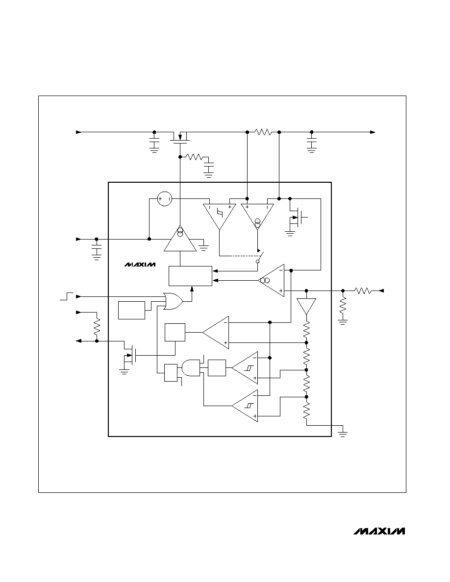
EN
OUT
10
RDSON
CURRENT
SENSE
ERROR
AMPLIFIER
REFIN
R1
R2
EN
C1
R6
PGOOD
THE MAX8737 INCLUDES TWO LDOs AS SHOWN ABOVE.
REF
GND
88%
80%
60%
CONTROL
BLOCK
DELAY
LOGIC
ILIM_EN
EN
Q
S
R
75
µs
DELAY
ILIM_EN
CS
DRV
0.4V
V
CC
MAX8737
C
IN
R3
N1
R
CS
C
OUT
4.7
µF/A
OUTPUT
C2
THERMAL
SHDN
5V BIAS
SUPPLY
INPUT
1.0V TO 5.5V
OFF ON
POWER
GOOD
LOGIC
SUPPLY
Figure 2. Functional Diagram
Slow UVP
If the output drops below 80% of the nominal output
voltage (V
REFIN
) for 75µs, the MAX8737 shuts down the
LDO and pulls the DRV_ pin to ground. If the output
voltage returns above 80% of the nominal output volt-
age (V
REFIN
) within the 75µs, the controller ignores the
load transient.
Fast UVP
If the output voltage drops below 60% of the nominal
output voltage (V
REFIN
) for approximately 5µs, the
MAX8737 immediately shuts down and pulls the DRV_
pin to ground. If the output voltage returns above 80%
of the nominal output voltage (V
REFIN
) within the 5µs,
the controller ignores the load transient.
Thermal Protection
The MAX8737 is available in a thin QFN package to
reduce the thermal impedance, and improve the ther-
mal coupling between the controller and the external
MOSFETs. When the controller's junction temperature
exceeds T
J
= +125°C (max), a thermal sensor turns off
the external pass transistor, allowing the system to
cool. The thermal sensor turns the pass transistor back
on once the controller's junction temperature drops by
approximately 20°C.
Design Procedure
Input Capacitor Selection (C
IN
)
Typically, the MAX8737 is powered from the output of a
step-down regulator, effectively providing a low-imped-
ance source. A local 10µF ceramic capacitor at V
IN
and
a 1.0µF ceramic capacitor at V
BIAS
should be sufficient
for most applications. If the linear regulator is connect-
ed to a high-impedance input, low-ESR polymer capac-
itors are recommended on the input.
Output Capacitor Selection (C
OUT
)
To maintain stability and provide good transient
response, the MAX8737 requires 4.7µF/A (4.7µF mini-
mum) of low ESR ceramic capacitor at the output. The
regulator remains stable with capacitances higher than
the minimum. When selecting the output capacitor to
MAX8737
Dual, Low-Voltage Linear Regulator Controllers
with External MOSFETs
______________________________________________________________________________________
11
V
OUT
C
OUT
R
CS
C
IN
INPUT
R3
C2
CS
OUT
DRV
MAX8737
MAX8737
V
OUT
C
OUT
R
CS
C
IN
INPUT
R3
C2
CS
OUT
DRV
R1
R2
10mV
R
CS
I
MAX
V
OUT
10mV
R
CS
I
MAX
V
OUT
SIMPLE CURRENT-LIMIT PROTECTION
FOLDBACK CURRENT-LIMIT PROTECTION
Figure 3. Current-Limit Protection
MAX8737
provide good transient response, the capacitor's ESR
should be minimized:
V
OUT
=
I
OUT
x ESR
where
I
OUT
is the maximum peak-to-peak load current
step, and
V
OUT
is the transient output-voltage tolerance.
Regulator Compensation
The compensation network (R3_, C2_) is customizable
and depends on load and MOSFET characteristics:
· Use of ceramic output capacitors with low R
ESR
to
ensure stability and minimize ESR voltage drop at
load step
· Strength of the external n-channel MOSFET (g
M
), its
forward transconductance (g
FS
), and the gate-to-
source capacitance (C
GS
)
· The driver transconductance (G
MDRV
) of the inte-
grated circuit driver
· Load current range (including the minimum load):
I
MIN
to I
MAX
Recommended Procedure
Use the C
GS
, g
FS,
I
D
from the chosen transistor data
sheet and use the equation below to translate the mea-
sured g
FS
to g
M
for normal operation:
1) Determine the LDO transconductance using the
MOSFET's forward transconductance (g
FS
), and the
drain current (I
D
) used to test the selected MOSFET:
2) Calculate the compensation resistor based on the
output capacitor (C
OUT
), the MOSFET's gate-to-
source capacitance (C
GS
= C
ISS
- C
RSS
), and the
minimum driver transconductance:
3) Calculate the compensation capacitance using the
minimum load current (I
MIN
) and compensation
resistor value calculated above:
where V
T
= 25mV.
Example: The example below is used to demonstrate
the stability calculation for the application circuit in
Figure 1.
1) Choose V
OUT
= 1.05V and I
MAX
= 3A and the mini-
mum load can be determined from the foldback cur-
rent-limit resistance:
2) For the selected MOSFET (Si4922DY), C
GS
=
2000pF at 1.5V, and g
FS
= 30S at I
D
= 8.8A:
3) The output capacitor must be at least 4.7µF/A.
Therefore the design must use a minimum 14.1µF
capacitor. The closest standard capacitor value is
22µF.
4) Based on the above operating conditions and com-
ponent selection, the compensation resistor value
should be:
5) Finally, select the compensation capacitor value:
External MOSFET Selection
The MAX8737 uses an n-channel MOSFET as the
series pass transistor instead of a p-channel MOSFET
to reduce cost. The selected MOSFET must have a
gate threshold voltage (at the required max load) that
meets the following criteria:
where V
CC
is the controller bias voltage, and V
GS_MAX
is the maximum gate voltage required to yield the on-
resistance (R
DS_ON
) specified by the manufacturer's
data sheet. Make sure that input-to-output voltage
meets the condition below to avoid entering dropout,
where output voltage starts to decrease and any ripple
on the input also passes through to the output. R
DSON
has a positive temperature coefficient (approximately
V
V
V
GS MAX
CC
OUT
_
-
C
mV
F
mA
S
F
2
2 25
22
6
1
35
0 15
2
=
×
×
× ×
=
µ
µ
(
)
.
R
F
nF
S
S
3
22
2
17 5
0 5
35
=
×
×
=
µ
.
.
g
S
A
A
S
M
=
=
30
3
8 8
17 5
.
.
I
V
R
R
mA
MIN
OUT
=
+
1
2
6
C
V C
I
G
R
T OUT
MIN MDRV
2
2
3
2
=
(
)
R
C
C
g
x
S
OUT
GS M
3
0 5
=
.
g
g
I
I
M
FS
MAX
D
=
Dual, Low-Voltage Linear Regulator Controllers
with External MOSFETs
12
______________________________________________________________________________________
0.5%/°C); therefore, the value of R
DSON
at the highest
operating junction temperature should be used:
where V
IN_MIN
is the minimum input voltage at the drain
of the MOSFET.
MOSFET Power Dissipation
The maximum power dissipation of the MAX8737
depends on the thermal resistance of the external n-
channel MOSFET package, the board layout, the tem-
perature difference between the die and ambient air,
and the rate of airflow. The power dissipated in the
MOSFET is:
P
DIS
= I
OUT
(V
IN
- V
CSP
)
The maximum allowable power dissipation is deter-
mined by the following formula:
where T
J(MAX)
is the maximum junction temperature
(+150°C), T
A
is the ambient temperature,
JC
is the
thermal resistance from the die junction to the package
case, and
CA
is the thermal resistance from the case
through the PC board, copper traces, and other materi-
als to the surrounding air. Standard 8-pin SO MOSFETs
are typically rated for 2W, while new power packages
(PowerPAKTM, DirectFETTM, etc.) can achieve power
dissipation ratings as high as 5W. For optimum power
dissipation, use a large ground plane with good ther-
mal contact to ground and use wide input and output
traces. Extra copper on the PC board increases ther-
mal mass and reduces the thermal resistance of the
board. See Figure 4.
PC Board Layout Guidelines
Due to the high-current paths and tight output accuracy
required by most applications, careful PC board layout
is required. An evaluation kit (MAX8737EVKIT) is avail-
able to speed design. It is important to keep all
traces as short as possible to minimize the high-
current trace dimensions to reduce the effect of
undesirable parasitic inductance. The MOSFET dissi-
pates a fair amount of heat due to the high currents
involved, especially during large input-to-output voltage
differences. To dissipate the heat generated by the
MOSFET, make power traces very wide with a large
amount of copper area. An efficient way to achieve
good power dissipation on a surface-mount package is
to lay out copper areas directly under the MOSFET
package on multiple layers and connect the areas
through vias. Use a ground plane to minimize imped-
ance and inductance.
In addition to the usual high-power considerations, here
are four tips to ensure high output accuracy:
· Ensure that the feedback connection to C
OUT
is
short and direct.
· Place the reference input resistors next to the
REFIN_ pin.
· Place RC and CC next to the DRV_ pin.
· Ensure REFIN_ and DRV_ traces are away from
noisy sources to ensure tight accuracy.
R
T
T
DIS MAX
J MAX
A
JC
CA
(
)
(
)
=
-
+
V
V
I
R
R
IN MIN
OUT MAX
MAX
DSON MAX
CS
_
_
_
(
)
-
+
MAX8737
Dual, Low-Voltage Linear Regulator Controllers
with External MOSFETs
______________________________________________________________________________________
13
PowerPAK is a registered trademark of Vishay Siliconix.
DirectFET is a trademark of International Rectifier Corp.

MAX8737
Dual, Low-Voltage Linear Regulator Controllers
with External MOSFETs
14
______________________________________________________________________________________
R6B
100k
POWER
GOOD 2
N2
R3B
33
C2B
0.22
µF
C
IN2
10
µF
C
SYS2
*
100
µF
C
OUT2
22
µF
1.05V
3A (MAX)
INPUT
1.25V TO 1.5V
ON
OFF
R9
100k
R8
42.2k
R7
47.5k
ON
OFF
R6A
100k
POWER
GOOD 1
C
IN1
10
µF
C
SYS1
*
100
µF
C
OUT1
10
µF
1.5V
2A (MAX)
C1
1.0
µF
5V BIAS
SUPPLY
INPUT
1.8V TO 2.5V
R3A
27
C2A
0.1
µF
GND
REFIN2
REFIN1
EN1
OUT1
DRV1
PGOOD1
CS1
V
CC
CS2
PGOOD2
DRV2
OUT2
EN2
MAX8737
NOTE: THE SYSTEM REFERENCE IS TYPICALLY
GENERATED BY THE STEP-DOWN CONVERTER
USED TO POWER THE DUAL LOW-VOLTAGE
LINEAR REGULATORS.
SYSTEM REF (2.0V)
N1
N1/N2: Si 4922DY
*A LOCAL 10
µF CERAMIC CAPACITOR IS SUFFICIENT
FOR MOST APPLICATIONS. IF THE MAX8737 IS POWERED
FROM A HIGH-IMPEDANCE SOURCE, ADDITIONAL LOW-ESR
POLYMER CAPACITORS ARE RECOMMENDED ON THE INPUT.
Figure 4. Typical Operating Circuit with Output Undervoltage Protection
Chip Information
TRANSISTOR COUNT: 1562
PROCESS: BiCMOS
MAX8737
Dual, Low-Voltage Linear Regulator Controllers
with External MOSFETs
Maxim cannot assume responsibility for use of any circuitry other than circuitry entirely embodied in a Maxim product. No circuit patent licenses are
implied. Maxim reserves the right to change the circuitry and specifications without notice at any time.
Maxim Integrated Products, 120 San Gabriel Drive, Sunnyvale, CA 94086 408-737-7600 ____________________ 15
© 2005 Maxim Integrated Products
Printed USA
is a registered trademark of Maxim Integrated Products, Inc.
Package Information
(The package drawing(s) in this data sheet may not reflect the most current specifications. For the latest package outline information,
go to www.maxim-ic.com/packages.)
24L QFN THIN.EPS
PACKAGE OUTLINE,
21-0139
2
1
D
12, 16, 20, 24, 28L THIN QFN, 4x4x0.8mm
PACKAGE OUTLINE,
21-0139
2
2
D
12, 16, 20, 24, 28L THIN QFN, 4x4x0.8mm