
_______________General Description
The MAX856MAX859 are high-efficiency, CMOS, step-
up, DC-DC switching regulators for small, low input volt-
age or battery-powered systems. The MAX856/MAX858
accept a positive input voltage between 0.8V and V
OUT
and convert it to a higher, pin-selectable output voltage of
3.3V or 5V. The MAX857/MAX859 adjustable versions
accept 0.8V to 6.0V input voltages and generate higher
adjustable output voltages in the 2.7V to 6.0V range.
Typical efficiencies are greater than 85%. Typical quies-
cent supply current is 25µA (1µA in shutdown).
The MAX856MAX859 combine ultra-low quiescent supply
current and high efficiency to give maximum battery life. An
internal MOSFET power transistor permits high switching
frequencies. This benefit, combined with internally set peak
inductor current limits, permits the use of small, low-cost
inductors. The MAX856/MAX857 have a 500mA peak
inductor current limit. The MAX858/MAX859 have a 125mA
peak inductor current limit.
________________________Applications
3.3V to 5V Step-Up Conversion
Palmtop Computers
Portable Data-Collection Equipment
Personal Data Communicators/Computers
Medical Instrumentation
2-Cell & 3-Cell Battery-Operated Equipment
Glucose Meters
____________________________Features
o
0.8V to 6.0V Input Supply Voltage
o
0.8V Typ Start-Up Supply Voltage
o
85% Efficiency at 100mA
o
25µA Quiescent Current
o
1µA Shutdown Mode
o
125mA and 500mA Switch-Current Limits Permit
Use of Low-Cost Inductors
o
Up to 500kHz Switching Frequency
o
±1.5% Reference Tolerance Over Temperature
o
Low-Battery Detector (LBI/LBO)
o
8-Pin SO and µMAX Packages
______________Ordering Information
Ordering Information continued at end of data sheet.
* Dice are tested at T
A
= +25°C only.
Contact factory for availability.
MAX856MAX859
3.3V/5V or Adjustable-Output,
Step-Up DC-DC Converters
________________________________________________________________
Maxim Integrated Products
1
1
2
3
4
8
7
6
5
LX
GND
OUT
LBI
LBO
REF
3/5
SHDN
MAX856
MAX858
SO/
µ
MAX
TOP VIEW
1
2
3
4
8
7
6
5
LX
GND
OUT
LBI
LBO
REF
FB
SHDN
MAX857
MAX859
SO/
µ
MAX
__________________Pin Configuration
MAX856
SHDN
3/5
REF
LX
GND
OUT
INPUT
0.8V TO V
OUT
1N5817
OUTPUT
5V AT 100mA
OR
3.3V AT 125mA
LBO
68
µ
F
47
µ
H
LOW-BATTERY
DETECTOR OUTPUT
ON/OFF
3V/5V SELECT
LBI
LOW-BATTERY
DETECTOR
INPUT
__________Typical Operating Circuit
19-0211; Rev 4; 5/96
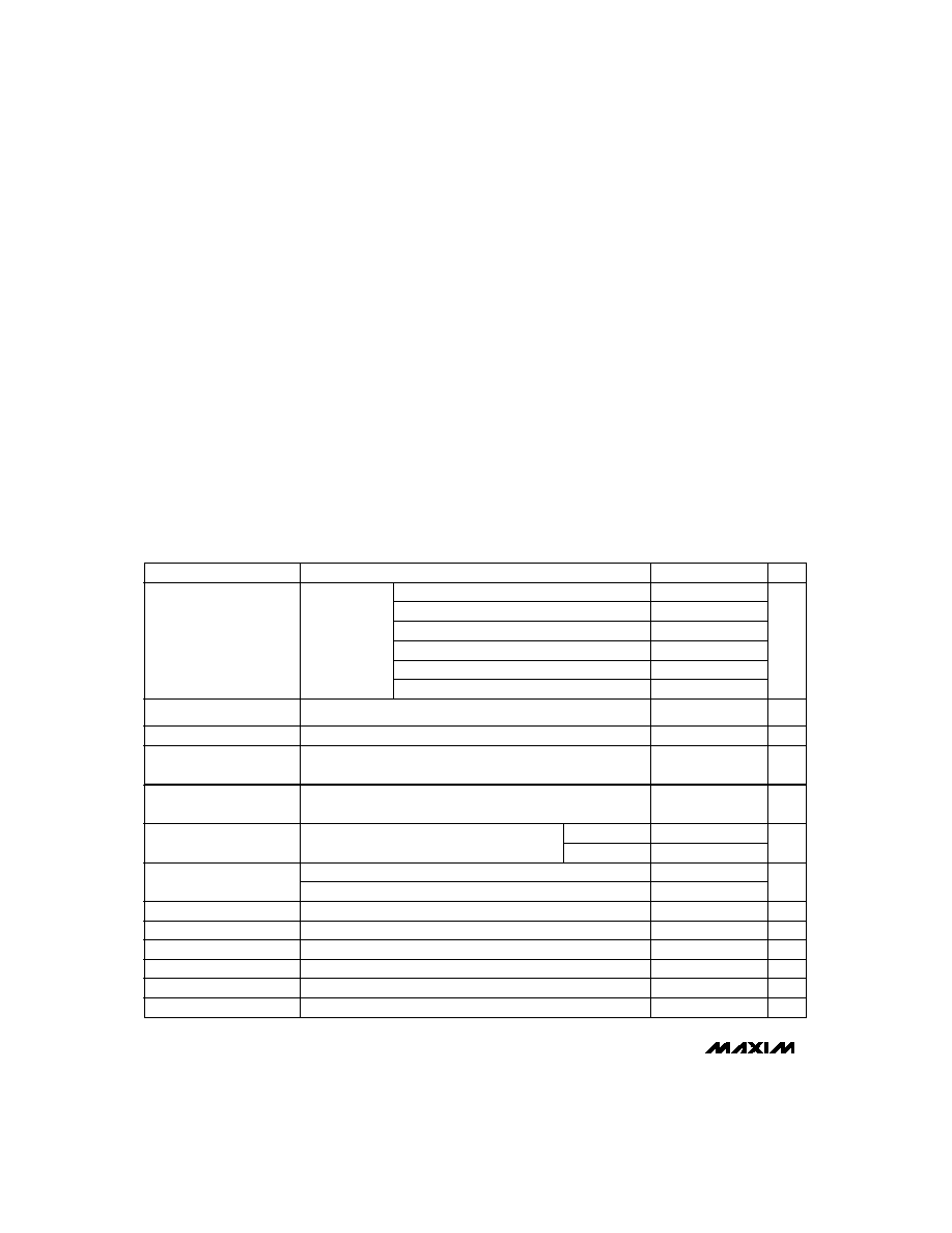
PART
TEMP. RANGE
PIN-PACKAGE
MAX856
CSA
0°C to +70°C
8 SO
MAX856CUA
0°C to +70°C
8 µMAX
MAX856C/D
0°C to +70°C
Dice*
MAX856ESA
-40°C to +85°C
8 SO
MAX856MJA
-55°C to +125°C
8 CERDIP
MAX857
CSA
0°C to +70°C
8 SO
MAX857CUA
0°C to +70°C
8 µMAX
MAX857C/D
0°C to +70°C
Dice*
MAX857ESA
-40°C to +85°C
8 SO
MAX857MJA
-55°C to +125°C
8 CERDIP
EVALUATION KIT MANUAL
FOLLOWS DATA SHEET
For free samples & the latest literature: http://www.maxim-ic.com, or phone 1-800-998-8800
MAX856MAX859
3.3V/5V or Adjustable-Output,
Step-Up DC-DC Converters
2
_______________________________________________________________________________________
ABSOLUTE MAXIMUM RATINGS
ELECTRICAL CHARACTERISTICS
(Circuits of Figure 2, V
IN
= 2.5V, I
LOAD
= 0mA, T
A
= T
MIN
to T
MAX
, unless otherwise noted. Typical values are at T
A
= +25°C.)
Stresses beyond those listed under "Absolute Maximum Ratings" may cause permanent damage to the device. These are stress ratings only, and functional
operation of the device at these or any other conditions beyond those indicated in the operational sections of the specifications is not implied. Exposure to
absolute maximum rating conditions for extended periods may affect device reliability.
Supply Voltage (OUT to GND) ...................................-0.3V, +7V
Switch Voltage (LX to GND) .......................................-0.3V, +7V
S
--
H
--
D
--
N
, LBO to GND ....................................................-0.3V, +7V
LBI, REF, 3/
5
, FB to GND .........................-0.3V, (V
OUT
+ 0.3V)
Reference Current (I
REF
) ..................................................2.5mA
Continuous Power Dissipation (T
A
= +70°C)
SO (derate 5.88mW/°C above +70°C) .........................471mW
µMAX (derate 4.1mW/°C above +70°C) ......................330mW
CERDIP (derate 8.00mW/°C above +70°C) .................640mW
Reverse Battery Current (T
A
+45°C, Note 1) .................750mA
Operating Temperature Ranges
MAX85_C_ _ ......................................................0°C to +70°C
MAX85_E_ _ ....................................................-40°C to +85°C
MAX85_MJA .................................................-55°C to +125°C
Junction Temperature .....................................................+150°C
Storage Temperature Range ............................-65°C to +160°C
Lead Temperature (soldering, 10sec) ............................+300°C
Note 1:
Reverse battery current is measured from the
Typical Operating Circuit's battery input terminal to GND when the battery is
connected backwards. A reverse current of 750mA will not exceed the SO or CERDIP package dissipation limits but, if left
for an extended time (more than ten minutes), may degrade performance.
LBO = 5V
I
SINK
= 2mA
With falling edge
3/
5
= 3V, -20µA
REF load
250µA, C
REF
= 0.22µF
No REF load
MAX858/MAX859
I
LOAD
= 0mA, 3/
5
= 3V, LBI = 1.5V, V
OUT
= 3.47V,
(FB = 1.5V, MAX857/MAX859 only)
MAX856/MAX857
S
--
H
--
D
--
N
= 0V, 3/
5
= 3V, LBI = 1.5V, V
OUT
= 3.47V,
(FB = 1.5V, MAX857/MAX859 only)
2V
V
IN
3V
I
LOAD
= 0mA
Output set for 3.3V, measured at V
IN
in Figure 2, R3 omitted.
CONDITIONS
µA
1
LBO Output Leakage Current
V
0.4
LBO Output Voltage Low
mV
25
LBI Input Hysteresis
V
1.22
1.25
1.28
LBI Input Threshold
%
0.8
2.0
Reference-Voltage Regulation
V
1.23
1.25
1.27
Reference Voltage
mA
125
500
µA
1
5
Shutdown Quiescent Current
(Note 2)
1
µA
60
No Load Battery Current
4.80
5.0
5.20
3.17
3.3
3.43
4.80
5.0
5.20
µA
25
60
Quiescent Supply Current in
3.3V Mode (Note 2)
V
0.8
Minimum Operating Voltage
4.80
5.0
5.20
3.17
3.3
3.43
V
4.80
5.0
5.20
Output Voltage
V
0.8
1.8
Minimum Start-Up
Supply Voltage
UNITS
MIN
TYP
MAX
PARAMETER
Peak Inductor Current Limit
MAX856, 3/
5
= 0V, 0mA
I
LOAD
100mA
MAX856, 3/
5
= 3V, 0mA
I
LOAD
150mA
MAX857, V
OUT
= 5V, 0mA
I
LOAD
100mA
MAX858, 3/
5
= 0V, 0mA
I
LOAD
25mA
MAX858, 3/
5
= 3V, 0mA
I
LOAD
35mA
MAX859, V
OUT
= 5V, 0mA
I
LOAD
25mA
MAX85_C
MAX85_E/M
MAX856MAX859
3.3V/5V or Adjustable-Output,
Step-Up DC-DC Converters
_______________________________________________________________________________________
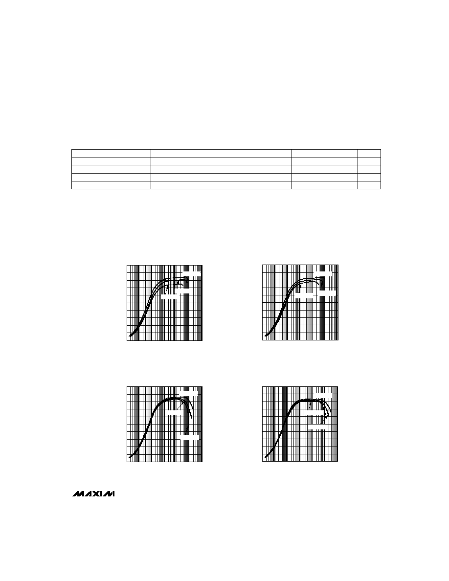
3
100
20
10
0
0.01
0.001
0.1
10
1
100
1000
MAX858/MAX859
EFFICIENCY vs. OUTPUT CURRENT
V
OUT
= 3.3V
40
30
50
MAX856-01
LOAD CURRENT (mA)
EFFICIENCY (%)
60
70
80
90
V
IN
= 2.0V
V
IN
= 2.5V
V
IN
= 1.5V
100
20
10
0
0.01
0.001
0.1
10
1
100
1000
MAX858/MAX859
EFFICIENCY vs. OUTPUT CURRENT
V
OUT
= 5V
40
30
50
MAX856-02
LOAD CURRENT (mA)
EFFICIENCY (%)
60
70
80
90
V
IN
= 2.5V
V
IN
= 3.3V
V
IN
= 1.5V
100
20
10
0
0.01
0.001
0.1
10
1
100
1000
MAX856/MAX857
EFFICIENCY vs. OUTPUT CURRENT
V
OUT
= 5V
40
30
50
MAX856-03
LOAD CURRENT (mA)
EFFICIENCY (%)
60
70
80
90
V
IN
= 2.0V
V
IN
= 3.3V
V
IN
= 1.5V
100
20
10
0
0.01
0.001
0.1
10
1
100
1000
MAX856/MAX857
EFFICIENCY vs. OUTPUT CURRENT
V
OUT
= 3.3V
40
30
50
MAX856-04
LOAD CURRENT (mA)
EFFICIENCY (%)
60
70
80
90
V
IN
= 2.0V
V
IN
= 2.5V
V
IN
= 1.5V
__________________________________________Typical Operating Characteristics
(Circuits of Figure 2, T
A
= +25°C, unless otherwise noted.)
ELECTRICAL CHARACTERISTICS (continued)
(Circuits of Figure 2, V
IN
= 2.5V, I
LOAD
= 0mA, T
A
= T
MIN
to T
MAX
, unless otherwise noted. Typical values are at T
A
= +25°C.)
Note 2:
Supply current from the 3.3V output is measured with an ammeter between the 3.3V output and OUT pin. This current
correlates directly with actual battery supply current, but is reduced in value according to the step-up ratio and efficiency.
V
OUT
= 3.47V to keep the internal switch open when measuring the current into the device.
Note 3:
Minimum value is production tested. Maximum value is guaranteed by design and is not production tested.
S
--
H
--
D
--
N
, 3/
5
Input Voltage Low
0.4
V
S
--
H
--
D
--
N
, 3/
5
Input Voltage High
1.6
V
S
--
H
--
D
--
N
, 3/
5
, FB, LBI Input Current
LBI = 1.5V, FB = 1.5V,
S
--
H
--
D
--
N
= 0V or 3V, 3/
5
= 0V or 3V
±100
nA
FB Voltage
MAX857/MAX859
1.22
1.25
1.28
V
Output Voltage Range
MAX857/MAX859, I
LOAD
= 0mA (Note 3)
2.7
6.0
V
MAX856MAX859
3.3V/5V or Adjustable-Output,
Step-Up DC-DC Converters
4
_______________________________________________________________________________________
_____________________________Typical Operating Characteristics (continued)
(Circuits of Figure 2, T
A
= +25°C, unless otherwise noted.)
0.75
0.1
10
MAX856/MAX857
MINIMUM START-UP INPUT VOLTAGE
vs. LOAD CURRENT
MAX856-06
LOAD CURRENT (mA)
START-UP INPUT VOLTAGE (V)
0.90
1.10
0.80
1.00
1
100
1.15
1.05
0.95
0.85
V
OUT
= 3.3V
V
OUT
= 5V
0.1
10
MAX858/MAX859
MINIMUM START-UP INPUT VOLTAGE
vs. LOAD CURRENT
MAX856-07
LOAD CURRENT (mA)
START-UP INPUT VOLTAGE (V)
0.9
1.3
1.1
1
100
1.4
1.2
1.0
0.8
V
OUT
= 5V
0.8
2.0
SHUTDOWN CURRENT
vs. INPUT VOLTAGE
0.7
MAX856-11
SHUTDOWN CURRENT (
µ
A)
0.5
1.5
0.6
2.5
3.0
0.4
0.3
0.2
0.1
0
3.5
4.0
INPUT VOLTAGE (V)
T
A
= +85°C
T
A
= +25°C
T
A
= -40°C
0.9
1.0
80
2.0
MAX858/MAX859
MAXIMUM OUTPUT CURRENT
vs. INPUT VOLTAGE
70
MAX856-12
LOAD CURRENT (mA)
50
1.5
60
2.5
3.0
40
30
20
10
0
3.5
4.0
INPUT VOLTAGE (V)
90
100
1.0
V
OUT
= 5.0V
V
OUT
= 3.3V
400
1.0
MAX856/MAX857
MAXIMUM OUTPUT CURRENT
vs. INPUT VOLTAGE
350
MAX856-13
LOAD CURRENT (mA)
250
300
2.0
1.5
2.5
200
150
100
50
0
3.0
3.5
4.0
INPUT VOLTAGE (V)
V
OUT
= 5.0V
V
OUT
= 3.3V
1.6
2.0
QUIESCENT CURRENT
vs. INPUT VOLTAGE
1.4
MAX856-10
QUIESCENT CURRENT (mA)
1.0
1.5
1.2
2.5
3.0
0.8
0.6
0.4
0.2
0
3.5
4.0
INPUT VOLTAGE (V)
SEE NOTE 2
IN THE ELECTRICAL
CHARACTERISTICS
T
A
= +85°C
T
A
= -40°C
1.6
2.0
MAX858/MAX859
NO LOAD BATTERY CURRENT
vs. INPUT VOLTAGE
1.4
MAX856-09
QUIESCENT CURRENT (mA)
1.0
1.5
1.2
2.5
3.0
0.8
0.6
0.4
0.2
0
3.5
4.0
INPUT VOLTAGE (V)
INCLUDES ALL EXTERNAL
COMPONENT LEAKAGES.
CAPACITOR LEAKAGE
DOMINATES AT T
A
= +85°C.
CAPS ARE SPRAGUE 595D
T
A
= +85°C
T
A
= +25°C
T
A
= -40°C
400
2.0
MAX856/MAX857
NO LOAD BATTERY CURRENT
vs. INPUT VOLTAGE
350
MAX856-08
QUIESCENT CURRENT (
µ
A)
250
1.5
300
2.5
3.0
200
150
100
50
0
3.5
4.0
INPUT VOLTAGE (V)
T
A
= +85°C
T
A
= +25°C
T
A
= -40°C
INCLUDES ALL EXTERNAL
COMPONENT LEAKAGES.
CAPACITOR LEAKAGE
DOMINATES AT T
A
= +85°C.
CAPS ARE SPRAGUE 595 D
5
0
REFERENCE VOLTAGE vs. CURRENT
6
10
MAX856-05
REFERENCE LOAD CURRENT (
µ
A)
V
REF
LOAD REGULATION (mV)
8
7
100
200
9
50
150
250
4
3
2
1
0
MAX856MAX859
3.3V/5V or Adjustable-Output,
Step-Up DC-DC Converters
_______________________________________________________________________________________
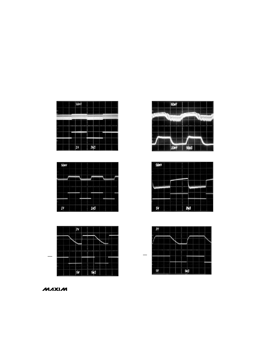
5
MAX856/MAX857
LINE-TRANSIENT RESPONSE (5V MODE)
2ms/div
V
OUT
50mV/div
V
IN
3V
2V
MAX856/MAX857
LOAD-TRANSIENT RESPONSE (5V MODE)
50
µ
s/div
V
OUT
50mV/div
0mA to 100mA
I
LOAD
V
IN
= 2.5V
MAX858/MAX859 LOAD-TRANSIENT RESPONSE
2ms/div
V
OUT
50mV/div
0mA to 25mA
I
LOAD
0
25
V
IN
= 2.5V
MAX859 LINE-TRANSIENT RESPONSE
1ms/div
V
OUT
50mV/div
1V/div
V
IN
3V
2V
MAX858/MAX859 START-UP DELAY (5V MODE)
5ms/div
V
OUT
2V/div
5V/div
V
SHDN
V
IN
= 2.5V, I
LOAD
= 25mA
MAX856 START-UP DELAY (5V MODE)
5ms/div
V
OUT
2V/div
5V/div
V
SHDN
V
IN
= 2.5V, I
LOAD
= 100mA
_____________________________Typical Operating Characteristics (continued)
(Circuits of Figure 2, T
A
= +25°C, unless otherwise noted.)