
General Description
The MAX8570 family of LCD step-up converters uses
an internal n-channel switch and an internal p-channel
output isolation switch. These converters operate from
a 2.7V to 5.5V supply voltage and deliver up to 28V at
the output.
A unique control scheme provides the highest efficien-
cy over a wide range of load conditions. The internal
MOSFET switch reduces external component count and
a high switching frequency (up to 800kHz) allows for
tiny surface-mount components. Three current-limit
options are available. The MAX8570 and MAX8572 use
a 110mA current limit to reduce ripple and component
size in low-current applications. For high-power require-
ments, the MAX8574 and MAX8575 use a 500mA cur-
rent limit and supply up to 20mA at 20V. The MAX8571
and MAX8573 use a 250mA current limit for a compro-
mise between ripple and power. Built-in safety features
protect the internal switch and down-stream compo-
nents from fault conditions.
Additional features include a low quiescent current and
a True Shutdown mode to save power. The MAX8570/
MAX8571/MAX8574 allow the user to set the output
voltage between 3V and 28V, and the MAX8572/
MAX8573/MAX8575 have a preset 15V output. These
step-up converters are ideal for small LCD panels with
low current requirements, but can also be used in other
applications. The MAX8571 evaluation kit is available to
help reduce design time.
Applications
LCD Bias Generators
Polymer LEDs (OLED)
Cellular or Cordless Phones
Palmtop Computers
Personal Digital Assistants (PDAs)
Organizers
Handy Terminals
Features
15V or Adjustable Output Voltage Up to 28V
Safety Features Protect Against Output Faults
20mA at 20V from a Single Li+ Battery
True Shutdown
87% Efficiency
Up to 800kHz Switching Frequency
Small 6-Pin SOT23 Package
MAX8570MAX8575
High-Efficiency LCD Boost
with True Shutdown
________________________________________________________________ Maxim Integrated Products
1
Ordering Information
19-3329; Rev 1; 10/04
For pricing, delivery, and ordering information, please contact Maxim/Dallas Direct! at
1-888-629-4642, or visit Maxim's website at www.maxim-ic.com.
EVALUATION KIT
AVAILABLE
PART
TEMP RANGE
PIN-
PACKAGE
TOP
MARK
MAX8570EUT-T
-40
°C to +85°C
6 SOT23-6
ABTJ
MAX8571EUT-T
-40
°C to +85°C
6 SOT23-6
ABTK
MAX8572EUT-T
-40
°C to +85°C
6 SOT23-6
ABTL
MAX8573EUT-T
-40
°C to +85°C
6 SOT23-6
ABTM
MAX8574EUT-T
-40
°C to +85°C
6 SOT23-6
ABTN
MAX8575EUT-T
-40
°C to +85°C
6 SOT23-6
ABTO
GND
LX
1
6
V
CC
5
SW
FB
MAX8570
MAX8571
MAX8574
SOT23-6
TOP VIEW
2
3
4
SHDN
GND
LX
1
6
V
CC
5
SW
OUT
MAX8572
MAX8573
MAX8575
SOT23-6
2
3
4
SHDN
Pin Configurations
PART
CURRENT LIMIT
OUTPUT VOLTAGE
MAX8570EUT
110mA
Adjustable
MAX8571EUT
250mA
Adjustable
MAX8572EUT
110mA
15V
MAX8573EUT
250mA
15V
MAX8574EUT
500mA
Adjustable
MAX8575EUT
500mA
15V
Selector Guide
True Shutdown is a trademark of Maxim Integrated Products,
Inc.
MAX8572
MAX8573
MAX8575
SW
V
CC
LX
OUT
GND
ON
OFF
V
CC
= 2.7V TO 5.5V
V
OUT
= V
CC
TO 28V
SHDN
Typical Operating Circuit

MAX8570MAX8575
High-Efficiency LCD Boost
with True Shutdown
2
_______________________________________________________________________________________
ABSOLUTE MAXIMUM RATINGS
ELECTRICAL CHARACTERISTICS
(V
CC
= V
SHDN
= 3.6V, SW floating, V
FB
= 1.3V (MAX8570/MAX8571/MAX8574) or V
OUT
= 16V (MAX8572/MAX8573/MAX8575), T
A
=
-40°C to +85°C, unless otherwise noted. Typical values are at T
A
= +25°C.) (Note 1)
Stresses beyond those listed under "Absolute Maximum Ratings" may cause permanent damage to the device. These are stress ratings only, and functional
operation of the device at these or any other conditions beyond those indicated in the operational sections of the specifications is not implied. Exposure to
absolute maximum rating conditions for extended periods may affect device reliability.
V
CC
, SHDN to GND ..................................................-0.3V to +6V
SW to GND .................................................-0.3V to (V
CC
+ 0.3V)
FB to GND (MAX8570/MAX8571/
MAX8574)...............................................-0.3V to (V
CC
+ 0.3V)
OUT to GND (MAX8572/MAX8573/MAX8575) .......-0.3V to +30V
LX to GND ..............................................................-0.3V to +30V
I
LX
, I
CC
..............................................................................600mA
Continuous Power Dissipation (T
A
= +70°C)
SOT23-6 (derate 8.7 mW/°C above +70°C).............695.7 mW
Operating Temperature Range ...........................-40°C to +85°C
Junction Temperature ......................................................+150°C
Storage Temperature Range .............................-65°C to +150°C
Lead Temperature (soldering, 10s) .................................+300°C
PARAMETER
CONDITIONS
MIN
TYP
MAX
UNITS
V
CC
Input Voltage Range
2.70
5.50
V
V
CC
Undervoltage Lockout
V
CC
rising, 50mV typical hysteresis
2.33
2.5
2.65
V
V
CC
Supply Current
25
35
µA
T
A
= +25
°C
0.05
1
V
CC
Shutdown Current
SHDN = GND, V
CC
= 5.5V
T
A
= -40
°C to +85°C
0.05
µA
Line Regulation
Circuit of Figure 3, V
OUT
= 15V, I
LOAD
= 5mA,
V
CC
= 2.7V to 5.5V
0.1
%/V
Load Regulation
Circuit of Figure 3, V
OUT
= 15V, I
LOAD
= 0 to 5mA
0.1
%/mA
T
A
= 0
°C to +85°C
1.216
1.226
1.236
FB Regulation Voltage
T
A
= -40
°C to +85°C
1.2137
1.2383
V
FB Input Bias Current
-50
-4
+50
nA
T
A
= 0
°C to +85°C
14.85
15
15.15
OUT Regulation Voltage
T
A
= -40
°C to +85°C
14.813
15.187
V
OUT Input Bias Current
V
OUT
= 15V
2.4
4.4
µA
LX Voltage Range
28
V
MAX8571/MAX8573
0.217
0.241
0.267
MAX8570/MAX8572
0.088
0.101
0.108
LX Switch Current Limit (Note 2)
MAX8574/MAX8575
0.425
0.484
0.540
A
MAX8571/MAX8573/MAX8574/MAX8575, I
LX
= 100mA
0.9
1.5
LX On-Resistance
MAX8570/MAX8572, I
LX
= 50mA
1.5
2.4
T
A
= +25
°C
0.01
2
LX Leakage Current
V
LX
= 28V
T
A
= -40
°C to +85°C
0.05
µA
Maximum LX On-Time
8
11
14
µs
V
FB
> 1V or V
OUT
> 12.2V
0.8
1
1.2
Minimum LX Off-Time
V
FB
= 0.25V or V
OUT
= 3.4V
4.0
5
6.0
µs
Current-Limit Propagation Delay
55
ns
SHDN Low Level (V
IL
)
2.7V
V
CC
5.5V
0.7
V
4.2V
V
CC
5.5V
1.5
SHDN High Level (V
IH
)
2.7V
V
CC
< 4.2V
1.4
V
SHDN Leakage Current
-1
+1
µA
MAX8570MAX8575
High-Efficiency LCD Boost
with True Shutdown
_______________________________________________________________________________________
3
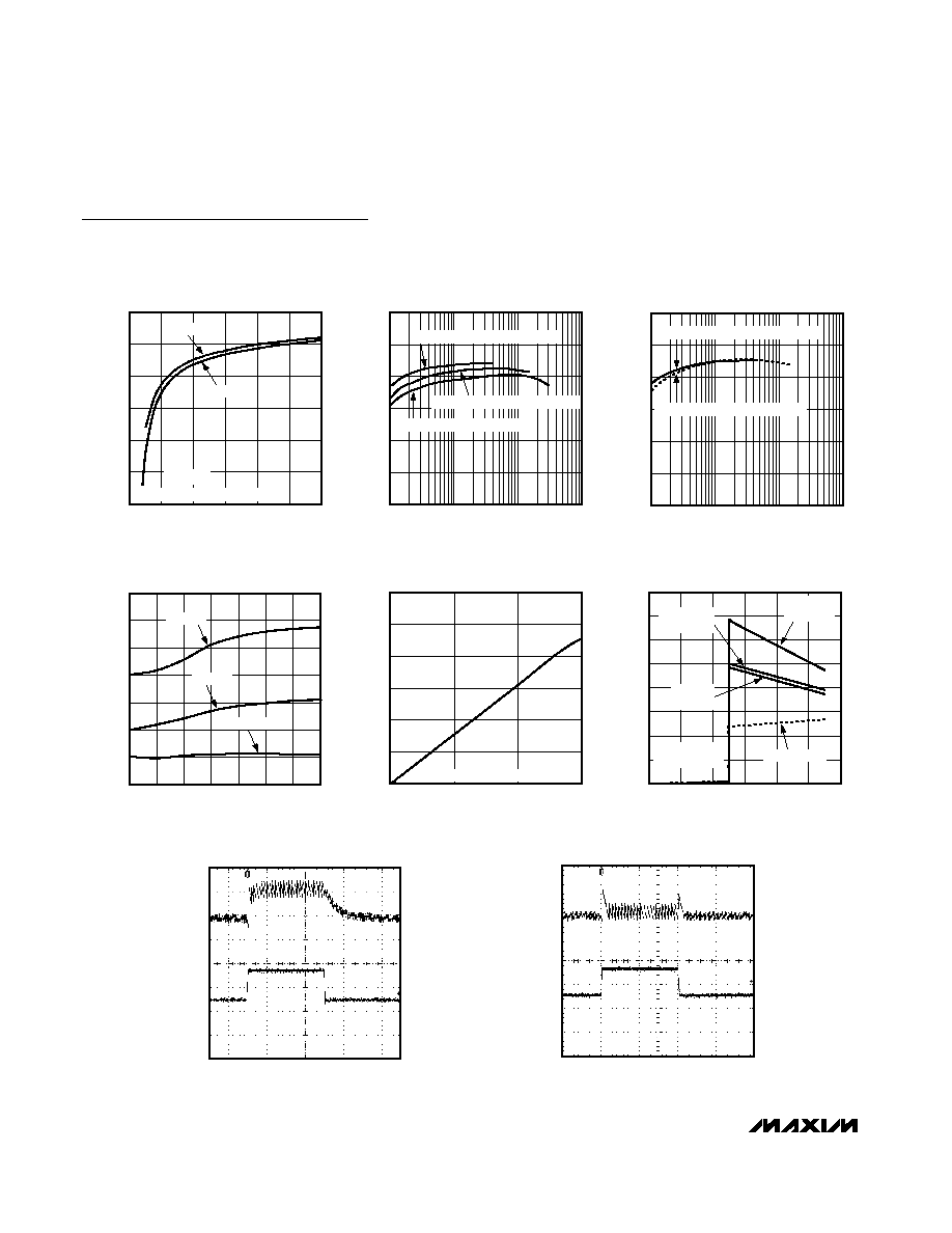
EFFICIENCY vs. SUPPLY VOLTAGE
MAX8570/71/73/74/75 toc06
SUPPLY VOLTAGE (V)
EFFICIENCY (%)
5.1
4.7
4.3
3.9
3.5
3.1
75
80
85
90
95
100
70
2.7
5.5
L1 = TOKO A914BYW-470M
47µH, 1mA LOAD
47µH, 5mA LOAD
L1 = MURATA LQH32CN220K23
22µH, 5mA LOAD
22µH, 1mA LOAD
Typical Operating Characteristics
(MAX8571, V
CC
= 3.6V, V
OUT
= 18V, Circuit of Figure 2, T
A
= +25°C, unless otherwise noted.)
OUTPUT VOLTAGE
vs. SUPPLY VOLTAGE (MAX8571)
MAX8570/71/73/74/75 toc01
SUPPLY VOLTAGE (V)
OUTPUT VOLTAGE (V)
5.1
4.7
3.9
4.3
3.5
3.1
17.6
17.7
17.8
17.9
18.0
18.1
18.2
18.3
18.4
18.5
17.5
2.7
5.5
L1 = MURATA LQH32CN220K23
R1 = 3.9M, R2 = 287k
5mA LOAD
1mA LOAD
OUTPUT VOLTAGE
vs. SUPPLY VOLTAGE (FIGURE 3, MAX8573)
MAX8570/71/73/74/75 toc02
SUPPLY VOLTAGE (V)
OUTPUT VOLTAGE (V)
5.1
4.7
3.9
4.3
3.5
3.1
14.6
14.7
14.8
14.9
15.0
15.1
15.2
15.3
15.4
15.5
14.5
2.7
5.5
L1 = MURATA LQH32CN220K23
5mA LOAD
1mA LOAD
OUTPUT VOLTAGE
vs. SUPPLY VOLTAGE (MAX8574)
MAX8570/71/73/74/75 toc03
SUPPLY VOLTAGE (V)
OUTPUT VOLTAGE (V)
4.6
4.3
4.0
3.7
3.4
17.2
18.2
18.0
17.8
17.6
17.4
18.4
18.6
18.8
19.0
17.0
3.1
4.9
L1 = TOKO S1024-100M
R1 = 1.1M, R2 = 75k, C4 = 4.7pF
5mA LOAD
20mA LOAD
OUTPUT VOLTAGE
vs. LOAD CURRENT
MAX8570/71/73/74/75 toc04
LOAD CURRENT (mA)
OUTPUT VOLTAGE (V)
20
15
5
10
17.6
17.8
18.0
18.2
18.4
18.6
18.8
19.0
17.4
0
25
L1 = MURATA LQH32CN220K23
R1 = 3.9M, R2 = 287k, C4 = 10pF
MAX8570
MAX8571
MAX8574, R1 = 1.1M, R2 = 75k, C4 = 4.7pF
OUTPUT VOLTAGE vs. TEMPERATURE
MAX8570/71/73/74/75 toc05
TEMPERATURE (°C)
OUTPUT VOLTAGE (V)
60
35
10
-15
17.7
17.8
17.9
18.0
18.1
18.2
18.3
18.4
17.6
-40
85
1mA LOAD
Note 1: Parameters are production tested at T
A
= +25°C. Limits over temperature are guaranteed by design.
Note 2: Specified currents are measured at DC. Actual LX current limits are slightly higher in circuit due to current-limit comparator
delay. Actual currents (with 2µH) are 110mA (MAX8570/MAX8572), 250mA (MAX8571/MAX8573), and 500mA
(MAX8574/MAX8575).
ELECTRICAL CHARACTERISTICS (continued)
(V
CC
= V
SHDN
= 3.6V, SW floating, V
FB
= 1.3V (MAX8570/MAX8571/MAX8574) or V
OUT
= 16V (MAX8572/MAX8573/MAX8575), T
A
=
-40°C to +85°C, unless otherwise noted. Typical values are at T
A
= +25°C.) (Note 1)
PARAMETER
CONDITIONS
MIN
TYP
MAX
UNITS
V
CC
= 3.6V, V
SW
= 0V, V
FB
= 0V, I
CC
(peak)
0.45
0.75
1.10
SW PMOS Current Limit
V
CC
= 3.6V, V
SW
= 0V, V
FB
= 0V, I
CC
(average)
0.15
0.30
0.60
A
SW PMOS On-Resistance
V
CC
= 2.7V, V
FB
= 0V, I
SW
= 100mA
1.5
2.5
T
A
= +25
°C
0.01
1
SW PMOS Leakage Current
SW = GND, V
CC
= 5.5V, V
FB
= 0V
T
A
= -40
°C to +85°C
0.02
µA
SW Soft-Start Time
V
CC
= 2.7V, C
SW
= 4.7µF
0.2
1
ms
MAX8570MAX8575
High-Efficiency LCD Boost
with True Shutdown
4
_______________________________________________________________________________________
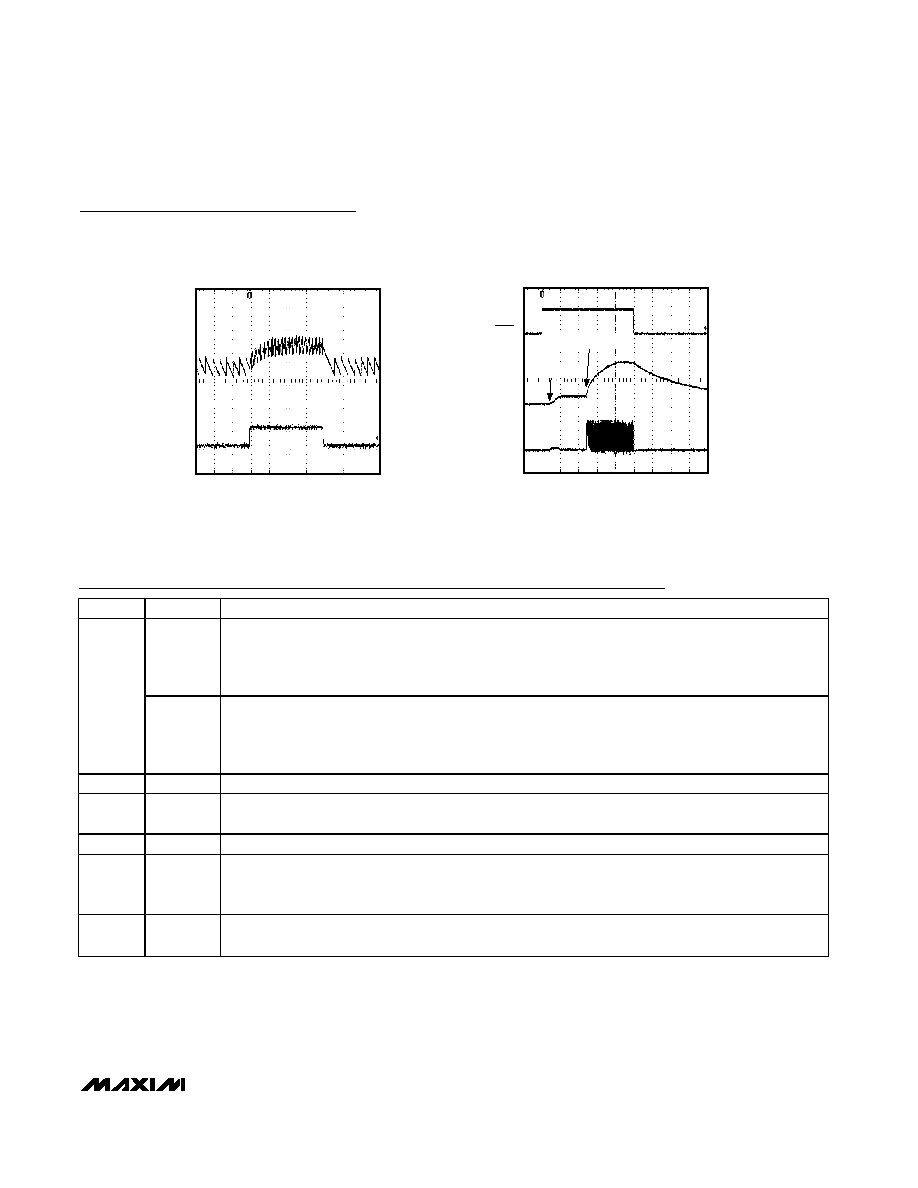
EFFICIENCY vs. BATTERY VOLTAGE
(FIGURE 4)
MAX8570/71/73/74/75 toc07
BATTERY VOLTAGE (V)
EFFICIENCY (%)
10
8
6
4
2
50
60
70
80
90
100
40
0
12
L1 = MURATA LQH32CN220K23
5mA LOAD
1mA LOAD
V
CC
= 3.6V
EFFICIENCY vs. LOAD CURRENT
WITH 22µH INDUCTOR
MAX8570/71/73/74/75 toc08
LOAD CURRENT (mA)
EFFICIENCY (%)
10
1
50
60
70
80
90
100
40
0.1
100
MAX8574, TOKO A914BYW-220M
MAX8571, MURATA LQH32CN220K23
MAX8570, MURATA LQH32CN220K23
EFFICIENCY vs. LOAD CURRENT
WITH 47µH INDUCTOR
MAX8570/71/73/74/75 toc09
LOAD CURRENT (mA)
EFFICIENCY (%)
10
1
50
60
70
80
90
100
40
0.1
100
MAX8570, L1 = MURATA LQH32CN470K23
MAX8571, L1 = TOKO A914BYW-470M
PEAK INDUCTOR CURRENT LIMIT
vs. SUPPLY VOLTAGE
MAX8570/71/73/74/75 toc10
SUPPLY VOLTAGE (V)
CURRENT LIMIT (mA)
5.1
4.7
4.3
3.9
3.5
3.1
100
200
300
400
500
600
700
0
2.7
5.5
MAX8574
MAX8571
MAX8570
SUPPLY CURRENT vs. LOAD CURRENT
MAX8570/71/73/74/75 toc11
LOAD CURRENT (mA)
SUPPLY CURRENT (mA)
10
5
20
40
60
80
100
120
0
0
15
L1 = MURATA LQH32CN220K23
NO-LOAD CURRENT vs. SUPPLY VOLTAGE
MAX8570/71/73/74/75 toc12
SUPPLY VOLTAGE (V)
SUPPLY CURRENT (
µ
A)
5
4
1
2
3
10
20
30
40
50
60
70
80
0
0
6
R1 = 3.9M
R2 = 287k
R1 = 7.87M
R2 = 576k
MAX8573,
FIGURE 3
L1 = MURATA
LQH32CN220K23
NO SWITCHING
LINE TRANSIENT 3V TO 5.5V (MAX8571)
MAX8570/71/73/74/75 toc13
100µs/div
V
CC
V
OUT
200mV/div
(AC-COUPLED)
2V/div
0
3.6k LOAD, R1 = 3.9M, R2 = 287k
LINE TRANSIENT 3V TO 5.5V
(FIGURE 3, MAX8573)
MAX8570/71/73/74/75 toc14
100µs/div
V
CC
V
OUT
200mV/div
(AC-COUPLED)
2V/div
0
3k LOAD
Typical Operating Characteristics (continued)
(MAX8571, V
CC
= 3.6V, V
OUT
= 18V, Circuit of Figure 2, T
A
= +25°C, unless otherwise noted.)
MAX8570MAX8575
High-Efficiency LCD Boost
with True Shutdown
_______________________________________________________________________________________
5
PIN
NAME
FUNCTION
FB
(MAX8570/
MAX8571/
MAX8574)
Feedback for setting the output voltage. Connect FB to the center of a resistor voltage-divider from the
output to GND to set positive output voltages.
1
OUT
(MAX8572/
MAX8573/
MAX8575)
Output. The output voltage is preset to 15V. Connect a 1µF ceramic capacitor from OUT to GND. In
shutdown, OUT is pulled to GND by an internal 7.5M
resistor.
2
GND
Ground
3
SHDN
Shutdown Input. A logic low at
SHDN places the part in low-power shutdown mode. Pull SHDN high or
connect to V
CC
for normal operation.
4
LX
Inductor Switching Connection
5
SW
Isolation Switch Output. Internally connected to the drain of a p-channel MOSFET used to isolate the
output from the input during shutdown. Connect a 4.7µF ceramic capacitor from SW to GND. If true
shutdown is not required, SW can be left open with the input supply connected directly to the inductor.
6
V
CC
Input Voltage Supply. Connect a 2.7V to 5.5V input supply to V
CC
. Connect a 1µF ceramic capacitor from
V
CC
to GND.
Pin Description
LOAD TRANSIENT
MAX8570/71/73/74/75 toc15
100µs/div
V
OUT
I
OUT
100mV/div
(AC-COUPLED)
5mA/div
0
STARTUP AND SHUTDOWN WAVEFORMS
MAX8570/71/73/74/75 toc16
400µs/div
V
OUT
I
LX
5V/div
10V/div
200mA/div
1.8 LOAD
0
0
V
SHDN
BOOST SOFT-START
SW TURN-ON
Typical Operating Characteristics (continued)
(MAX8571, V
CC
= 3.6V, V
OUT
= 18V, Circuit of Figure 2, T
A
= +25°C, unless otherwise noted.)