MAX8569 DS (JOSE-NEW LAYOUT)
General Description
The MAX8569A/MAX8569B low-quiescent-current
boost regulators provide up to 200mA at output volt-
ages up to 5.5V from a 1.5V to 5.5V input source. The
built-in synchronous rectifier allows for over 90% effi-
ciency while achieving small size and low cost by elimi-
nating the need for an external Schottky diode.
The MAX8569A provides an adjustable output while the
MAX8569B is fixed at 3.0V or 3.3V. The MAX8569B fea-
tures a power-on reset output (RST) to signal that the
output has reached regulation. All devices connect the
battery input to the output during shutdown, allowing
the input battery to be used as a backup or real-time
clock supply when the converter is off.
Applications
Features
o Over 200mA Available Output Current
o 1.5V to 5.5V Input Voltage Range
o BATT Connected to OUT in Shutdown for Backup
Power
o Up to 95% Efficiency
o 7µA Typical Quiescent Current
o <1µA Shutdown Supply Current
o Internal Synchronous Rectifier
o 750mA Switch Current Limit
o RST Output (MAX8569B)
o Adjustable Output Voltage (MAX8569A)
o Fixed 3.0V or 3.3V Output Voltage (MAX8569B)
MAX8569A/MAX8569B
200mA Step-Up Converters in 6-Pin
SOT23 and TDFN
________________________________________________________________ Maxim Integrated Products
1
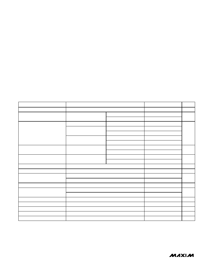
MAX8569A
(MAX8569B)
TOP VIEW
6
FB (RST)
5
OUT
4
LX
SHDN
BATT
GND
1
2
3
TDFN
( ) ARE FOR THE MAX8569B
1
6
5
MAX8569A
(MAX8569B)
TOP VIEW
SOT23
2
3
4
FB (RST)
OUT
LX
SHDN
BATT
GND
+
+ DENOTES LEAD-FREE PACKAGING
Pin Configurations
Ordering Information
19-3671; Rev 0; 5/05
For pricing, delivery, and ordering information, please contact Maxim/Dallas Direct! at
1-888-629-4642, or visit Maxim's website at www.maxim-ic.com.
EVALUATION KIT
AVAILABLE
PART
TEMP RANGE
PIN-PACKAGE
MAX8569AEUT-T*
-40°C to +85°C
6 SOT23-6
(U6FH-6)
MAX8569AETT+
-40°C to +85°C
6 TDFN 3mm x 3mm
(T633-1)
MAX8569BEUT-T*
-40°C to +85°C
6 SOT23-6
(U6FH-6)
MAX8569BETT+
-40°C to +85°C
6 TDFN 3mm x 3mm
(T633-1)
MAX8569BETT30+
-40°C to +85°C
6 TDFN 3mm x 3mm
(T633-1)
Selector Guide appears at end of data sheet.
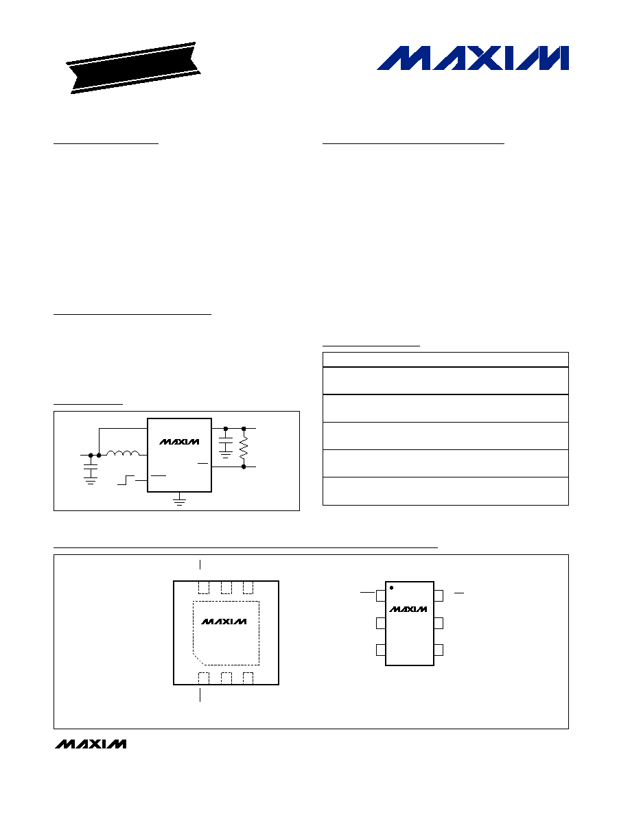
MAX8569B
RST
OUT
2V
INPUT
3.3V, 200mA
OUTPUT
POWER-ON
RESET
LX
OFF
ON
SHDN
BATT
GND
Typical Operating Circuit
Medical Diagnostic
Equipment
Digital Cameras
PDAs and Smartphones
Cordless Phones
Battery Backup
PC Cards
Local 3.3V or 5V Supply
*Future product--contact factory for availability.
+Denotes lead-free packaging.
MAX8569A/MAX8569B
200mA Step-Up Converters in 6-Pin
SOT23 and TDFN
2
_______________________________________________________________________________________
ABSOLUTE MAXIMUM RATINGS
ELECTRICAL CHARACTERISTICS
(V
SHDN
= V
OUT
= 3.3V, V
BATT
= 2.0V, T
A
= -40°C to +85°C. Typical values are at T
A
= +25°C, unless otherwise noted.) (Note 1)
Stresses beyond those listed under "Absolute Maximum Ratings" may cause permanent damage to the device. These are stress ratings only, and functional
operation of the device at these or any other conditions beyond those indicated in the operational sections of the specifications is not implied. Exposure to
absolute maximum rating conditions for extended periods may affect device reliability.
BATT, LX, OUT, FB, RST to GND .............................-0.3V to +6V
SHDN to GND...........................................-0.3V to (V
OUT
+ 0.3V)
LX Current ....................................................................1.5A Peak
Continuous Power Dissipation (T
A
= +70°C)
6-Pin SOT23 (derate 9.1mW/°C above +70°C)............727mW
6-Pin TDFN 3mm x 3mm
(derate 18.2mW/°C above +70°C) .............................1454mW
Operating Temperature Range ...........................-40°C to +85°C
Junction Temperature ......................................................+150°C
Storage Temperature Range .............................-65°C to +150°C
Lead Temperature (soldering, 10s) .................................+300°C
PARAMETER
CONDITIONS
MIN
TYP
MAX
UNITS
Battery Input Range
1.5
5.5
V
T
A
= +25°C
1.22
1.5
Startup Voltage
R
LOAD
= 2.6k
T
A
= -40°C to +85°C
1.24
V
MAX8569A
2.0
5.5
T
A
= +25°C
2.94
3.0
3.06
MAX8569BETT30
T
A
= -40°C to +85°C
2.925
3.075
T
A
= +25°C
3.233
3.300
3.366
Output Voltage
MAX8569B
T
A
= -40°C to +85°C
3.217
3.373
V
T
A
= +25°C
1.208
1.228
1.248
Feedback Threshold
MAX8569A
T
A
= -40°C to +85°C
1.203
1.253
V
T
A
= +25°C
3.5
20
Feedback Bias Current
MAX8569A, V
FB
= 1.27V
T
A
= -40°C to +85°C
4
nA
n-Channel On-Resistance
I
LX
= 100mA
0.3
0.7
p-Channel On-Resistance
I
LX
= 100mA
0.3
0.9
T
A
= +25°C
650
750
920
n-Channel Switch Current Limit
T
A
= -40°C to +85°C
600
975
mA
Switch Maximum On-Time
V
OUT
= 2.8V
3.5
5
6.5
µs
T
A
= +25°C
3
25
50
Synchronous Rectifier Zero-
Crossing Current
T
A
= -40°C to +85°C
0
60
mA
OUT Quiescent Current
V
OUT
= 3.5V, V
FB
= 1.3V (Note 2)
4
10
µA
OUT Shutdown Current
V
OUT
= 3.5V, V
SHDN
= V
FB
= 0V
0.05
1
µA
BATT Quiescent Current
V
OUT
= 3.5V, V
FB
= 1.3V (Note 3)
3
10
µA
BATT Shutdown Current
V
OUT
= 3.5V, V
SHDN
= 0V
0.01
1
µA
SHDN Logic-Low
0.3
V
MAX8569A/MAX8569B
200mA Step-Up Converters in 6-Pin
SOT23 and TDFN
_______________________________________________________________________________________
3
ELECTRICAL CHARACTERISTICS (continued)
(V
SHDN
= V
OUT
= 3.3V, V
BATT
= 2.0V, T
A
= -40°C to +85°C. Typical values are at T
A
= +25°C, unless otherwise noted.) (Note 1)
Note 1: Specifications to -40°C are guaranteed by design and not production tested.
Note 2: Supply current into OUT. This current is drawn from the source battery, but is reduced in value according to the step-up
ratio and efficiency.
Note 3: Does not include switching losses and output quiescent current. See the Input Current and Output Voltage vs. Input Voltage
(On, 330
) graph in the Typical Operating Characteristics for operating quiescent current.
PARAMETER
CONDITIONS
MIN
TYP
MAX
UNITS
T
A
= +25°C
1.185
1.228
1.271
SHDN Threshold
Rising edge,
100mV hysteresis (typ),
V
OUT
= 2.8V
T
A
= -40°C to +85°C
1.170
1.286
V
T
A
= +25°C
13
100
SHDN Input Bias Current
V
OUT
= 5.5V
T
A
= -40°C to +85°C
13
nA
RST Low Voltage
I
RST
= 1mA, V
OUT
= 2.5V
0.2
V
T
A
= +25°C
0.1
100
RST Leakage Current
V
RST
= 5.5V
T
A
= -40°C to +85°C
1
nA
T
A
= +25°C
85
90
95
RST Threshold
Relative to OUT,
3.3V for MAX8569B,
3.0V for MAX8569BETT30
T
A
= -40°C to +85°C
85
90
97
%
T
A
= +25°C
1
150
LX Leakage Current
V
OUT
= 5.5V
T
A
= -40°C to +85°C
150
nA
Maximum Load Current
V
BATT
= 2V, V
OUT
= 3.3V
200
mA
Efficiency
V
BATT
= 2V, V
OUT
= 3.3V, Figures 1 or 2, I
LOAD
= 40mA
88
%
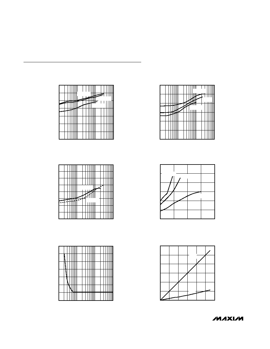
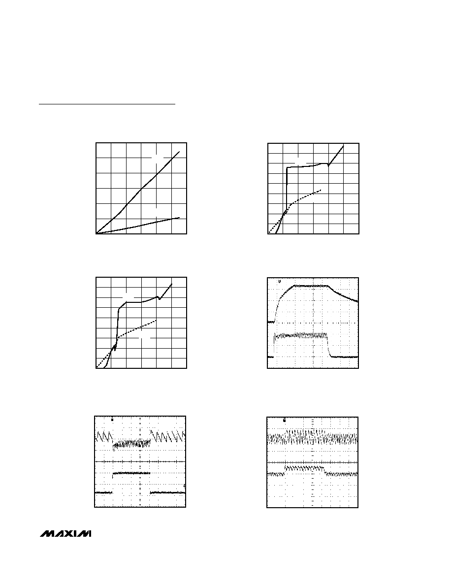
OUTPUT VOLTAGE AND INPUT CURRENT
vs. INPUT VOLTAGE (SHUTDOWN, NO LOAD)
MAX8569 toc06
BATTERY VOLTAGE (V)
OUTPUT VOLTAGE (V)
BATTERY CURRENT (
µ
A)
5
4
3
2
1
1
2
3
4
5
6
0
1
2
3
4
5
6
0
0
6
V
OUT
I
BATT
Typical Operating Characteristics
(Circuit of Figure 2, V
OUT
= 3.3V, V
BATT
= +2V, T
A
= +25°C, circuit of Figure 1, T
A
= +25°C, unless otherwise noted.)
MAX8569A/MAX8569B
200mA Step-Up Converters in 6-Pin
SOT23 and TDFN
4
_______________________________________________________________________________________
MAXIMUM OUTPUT CURRENT
vs. BATTERY VOLTAGE
MAX8569 toc04
BATTERY VOLTAGE (V)
MAXIMUM OUTPUT CURRENT (mA)
5.5
4.5
3.5
2.5
100
200
300
400
500
600
0
1.5
V
OUT
= 2.5V
V
OUT
= 5V
V
OUT
= 3.3V
100
1
100
1000
V
IN
= 4.2V
V
IN
= 3.3V
V
IN
= 2.5V
EFFICIENCY vs. LOAD CURRENT
V
OUT
= 5V
70
65
75
80
85
90
95
MAX8569 toc01
LOAD CURRENT (mA)
EFFICIENCY (%)
10
1
100
1000
EFFICIENCY vs. LOAD CURRENT
V
OUT
= 3.3V
70
65
75
80
85
90
95
MAX8569 toc02
LOAD CURRENT (mA)
EFFICIENCY (%)
10
V
IN
= 2V
V
IN
= 1.5V
V
IN
= 2.5V
10
1k
10k
STARTUP VOLTAGE vs. LOAD RESISTANCE
MAX8569 toc05
R
LOAD
(
)
STARTUP VOLTAGE (V)
100
1.34
1.20
1.22
1.24
1.26
1.28
1.32
1.30
100
60
1
100
1000
EFFICIENCY vs. LOAD CURRENT
V
OUT
= 2.5V
70
65
75
80
85
90
95
MAX8569 toc03
LOAD CURRENT (mA)
EFFICIENCY (%)
10
V
IN
= 2V
V
IN
= 1.5V
MAX8569A/MAX8569B
200mA Step-Up Converters in 6-Pin
SOT23 and TDFN
_______________________________________________________________________________________
5
OUTPUT VOLTAGE AND INPUT CURRENT
vs. INPUT VOLTAGE (SHUTDOWN, 200mA LOAD)
MAX8569 toc07
BATTERY VOLTAGE (V)
OUTPUT VOLTAGE (V)
BATTERY CURRENT (
µ
A)
5
4
3
2
1
1
2
3
4
5
6
0
1
2
3
4
5
6
0
0
6
V
OUT
I
BATT
OUTPUT VOLTAGE AND INPUT CURRENT
vs. INPUT VOLTAGE (ON, 330
)
MAX8569 toc08
BATTERY VOLTAGE (V)
OUTPUT VOLTAGE (V)
BATTERY CURRENT (
µ
A)
4
2
0.5
1.0
1.5
2.0
2.5
3.0
3.5
4.0
4.5
0
0.5
1.0
1.5
2.0
2.5
3.0
3.5
4.0
4.5
0
0
1
3
5
6
V
OUT
I
BATT
OUTPUT VOLTAGE AND INPUT CURRENT
vs. INPUT VOLTAGE (ON, 16
LOAD)
MAX8569 toc09
BATTERY VOLTAGE (V)
OUTPUT VOLTAGE (V)
BATTERY CURRENT (
µ
A)
4
2
0
1
3
5
6
0.5
1.0
1.5
2.0
2.5
3.0
3.5
4.0
4.5
0
0.5
1.0
1.5
2.0
2.5
3.0
3.5
4.0
4.5
0
V
OUT
I
BATT
ON/OFF RESPONSE (R
LOAD
= 33
)
MAX8569 toc10
1V/div
1V/div
V
OUT
V
IN
100
µs/div
LOAD TRANSIENT
MAX8569 toc11
100mV/div
200mA
20mA
V
OUT
(AC-COUPLED)
I
OUT
100
µs/div
LINE TRANSIENT
MAX8569 toc12
100mV/div
2.5V
2V
V
OUT
(AC-COUPLED)
V
IN
100ms/div
Typical Operating Characteristics (continued)
(Circuit of Figure 2, V
OUT
= 3.3V, V
BATT
= +2V, T
A
= +25°C, circuit of Figure 1, T
A
= +25°C, unless otherwise noted.)