
_______________General Description
The MAX823/MAX824/MAX825* microprocessor (µP)
supervisory circuits combine reset output, watchdog,
and manual-reset input functions in a 5-pin SOT23-5
package. They significantly improve system reliability
and accuracy compared to separate ICs or discrete
components. The MAX823/MAX824/MAX825 are
specifically designed to ignore fast transients on V
CC
.
Five preprogrammed reset threshold voltages are
available, designated by the following package
suffixes: L = 4.63V, M = 4.38V, T = 3.08V, S = 2.93V,
and R = 2.63V. All three devices have an active-low
reset output, which is guaranteed to be in the correct
state for V
CC
down to 1V. The MAX824/MAX825 also
have an active-high reset output. The following
Selector
Guide explains the functions offered in this series of
parts.
________________________Applications
Battery-Powered Computers and Controllers
Embedded Controllers
Intelligent Instruments
Automotive Systems
Critical µP Monitoring
Portable/Battery-Powered Equipment
____________________________Features
o
Precision Monitoring of +3V, +3.3V, and +5V
Power Supplies
o
Operating Current: 10µA (MAX823L/M)
3µA (MAX825T/S/R)
o
Fully Specified Over Temperature
o
140ms Min Power-On Reset
o
Guaranteed RESET Valid to V
CC
= 1V
o
Power-Supply Transient Immunity
o
Watchdog Timer with 1.6sec Timeout
(MAX823/MAX824)
o
Manual-Reset Input (MAX823/MAX825)
o
No External Components
MAX823/MAX824/MAX825
5-Pin Microprocessor Supervisory Circuits
________________________________________________________________
Maxim Integrated Products
1
1
5
2
3
4
1
5
2
3
4
1
5
2
3
4
GND
WDI
MR
V
CC
RESET
MAX823
SOT23-5
TOP VIEW
GND
WDI
RESET
V
CC
RESET
MAX824
SOT23-5
GND
MR
RESET
V
CC
RESET
MAX825
SOT23-5
__________________________________________________________Pin Configurations
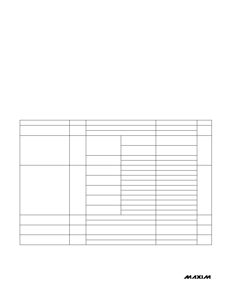
_____________________Selector Guide
19-0487; Rev 1; 6/97
PART
MAX823_EUK
MAX824_EUK
-40°C to +85°C
-40°C to +85°C
TEMP. RANGE
PIN-PACKAGE
5 SOT23-5
5 SOT23-5
______________Ordering Information
Insert the desired suffix letter (from the table below) into the
blank to complete the part number.
For free samples & the latest literature: http://www.maxim-ic.com, or phone 1-800-998-8800.
For small orders, phone 408-737-7600 ext. 3468.
MAX825_EUK
-40°C to +85°C
5 SOT23-5
MAX823
Active-Low Reset
Active-High Reset
--
FUNCTION
Watchdog Input
MAX824
MAX825
--
Manual-Reset Input
--
SUFFIX
RESET
THRESHOLD (V)
L
4.63
M
4.38
T
3.08
S
2.93
R
2.63
Typical Operating Circuit appears at end of data sheet.
Marking Information appears at end of data sheet.
*Patents Pending
MAX823/MAX824/MAX825
5-Pin Microprocessor Supervisory Circuits
2
_______________________________________________________________________________________
ABSOLUTE MAXIMUM RATINGS
ELECTRICAL CHARACTERISTICS
(V
CC
= +4.75V to +5.5V for MAX82_L, V
CC
= +4.5V to +5.5V for MAX82_M, V
CC
= +3.15V to +3.6V for MAX82_T, V
CC
= +3V
to +3.6V for MAX82_S, V
CC
= +2.7V to +3.6V for MAX82_R, T
A
= T
MIN
to T
MAX
, unless otherwise noted. Typical values are at
T
A
= +25°C.) (Note 1)
Stresses beyond those listed under "Absolute Maximum Ratings" may cause permanent damage to the device. These are stress ratings only, and functional
operation of the device at these or any other conditions beyond those indicated in the operational sections of the specifications is not implied. Exposure to
absolute maximum rating conditions for extended periods may affect device reliability.
V
CC
........................................................................-0.3V to +6.0V
All Other Pins..............................................-0.3V to (V
CC
+ 0.3V)
Input Current, All Pins Except RESET and RESET..............20mA
Output Current, RESET, RESET ..........................................20mA
Rate of Rise, V
CC
............................................................100V/µs
Continuous Power Dissipation (T
A
= +70°C)
SOT23-5 (derate 7.1mW/°C above +70°C)...................571mW
Operating Temperature Range
MAX82_EUK .....................................................-40°C to +85°C
Storage Temperature Range .............................-65°C to +160°C
Lead Temperature (soldering, 10sec) .............................+300°C
MAX82_M
T
A
= +25°C
T
A
= -40°C to +85°C
WDI and MR
unconnected
4.25
4.50
T
A
= -40°C to +85°C
T
A
= 0°C to +70°C
4.31
4.38
4.45
MAX82_T/S/R
MAX82_L/M
MAX82_L
T
A
= +25°C
T
A
= -40°C to +85°C
MR unconnected
MAX82_S
CONDITIONS
T
A
= +25°C
T
A
= -40°C to +85°C
2.85
3.00
2.89
2.93
2.96
MAX82_T
T
A
= +25°C
T
A
= -40°C to +85°C
3.00
3.15
3.04
3.08
3.11
MAX82_L/M
MAX82_T/S/R
mV
5
Reset Threshold Hysteresis
10
MAX82_R
T
A
= +25°C
T
A
= -40°C to +85°C
V
2.55
2.70
V
RST
Reset Threshold
2.59
2.63
2.66
MAX823T/S/R,
MAX824T/S/R
5
12
V
1.2
V
CC
1.0
5.5
MAX823L/M,
MAX824L/M
MAX825L/M
Operating Voltage Range
ms
140
200
280
t
RP
Reset Timeout Period
140
200
280
ppm/°C
40
Reset Threshold Temperature
Coefficient
4.50
4.75
10
24
4.5
12
µA
3
8
I
SUPPLY
Supply Current
4.56
4.63
4.70
UNITS
MIN
TYP
MAX
SYMBOL
PARAMETER
MAX825T/S/R
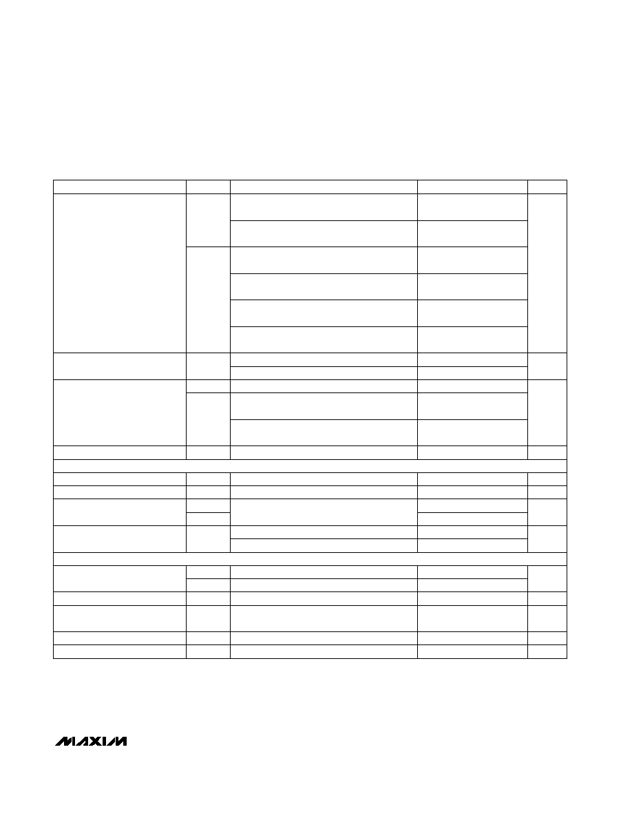
ELECTRICAL CHARACTERISTICS (continued)
(V
CC
= +4.75V to +5.5V for MAX82_L, V
CC
= +4.5V to +5.5V for MAX82_M, V
CC
= +3.15V to +3.6V for MAX82_T, V
CC
= +3V
to +3.6V for MAX82_S, V
CC
= +2.7V to +3.6V for MAX82_R, T
A
= T
MIN
to T
MAX
, unless otherwise noted. Typical values are at
T
A
= +25°C.) (Note 1)
Note 1:
Over-temperature limits are guaranteed by design and not production tested.
Note 2:
The RESET short-circuit current is the maximum pull-up current when RESET is driven low by a µP bidirectional reset pin.
Note 3:
WDI is internally serviced within the watchdog period if WDI is left unconnected.
Note 4:
The WDI input current is specified as the average input current when the WDI input is driven high or low. The WDI input is
designed to drive a three-stated-output device with a 10µA maximum leakage current and a maximum capacitive load of
200pF. This output device must be able to source and sink at least 200µA when active.
MAX823/MAX824/MAX825
5-Pin Microprocessor Supervisory Circuits
_______________________________________________________________________________________
3
V
RST
- V
CC
= 100mV
MAX824T/S/R, MAX825T/S/R,
V
CC
= V
RST
max, I
SINK
= 1.2mA
MAX82_L/M, V
CC
= V
RST
max,
I
SOURCE
= 120µA
MAX824L/M, MAX825L/M,
V
CC
= V
RST
max, I
SINK
= 3.2mA
V
CC
> 1.8V, I
SOURCE
= 150µA
MAX82_L/M, RESET = 0V, V
CC
= 5.5V
CONDITIONS
µs
20
V
CC
to RESET Delay
V
0.3
V
OL
RESET Output Voltage
V
CC
- 1.5
0.4
0.8V
CC
V
OH
800
UNITS
MIN
TYP
MAX
SYMBOL
PARAMETER
MAX82_T/S/R, V
CC
= V
RST
max,
I
SOURCE
= 30µA
0.8V
CC
V
OH
MAX82_T/S/R, V
CC
= V
RST
min,
I
SINK
= 1.2mA
MAX82_L/M, V
CC
= V
RST
min,
I
SINK
= 3.2mA
0.3
0.4
T
A
= -40°C to +85°C, V
CC
= 1.2V,
V
CC
falling, V
BATT
= 0V, I
SINK
= 100µA
T
A
= 0°C to +70°C, V
CC
= 1V,
V
CC
falling, I
SINK
= 50µA
V
0.3
V
OL
RESET Output Voltage
0.3
MAX82_T/S/R, RESET = 0V, V
CC
= 3.6V
µA
400
I
SOURCE
RESET Output Short-Circuit
Current (Note 2)
V
IL
= 0.4V, V
IH
= 0.8V
CC
ns
50
t
WDI
WDI Pulse Width
sec
1.12
1.60
2.40
t
WD
Watchdog Timeout Period
WDI = 0V, time average
WDI = V
CC
, time average
V
CC
= 5V
µA
-20
-15
WDI Input Current (Note 4)
120
160
V
0.7V
CC
V
IH
WDI Input Threshold (Note 3)
0.3V
CC
V
IL
µs
1.0
MR Pulse Width
V
0.7V
CC
V
IH
MR Input Threshold
0.3V
CC
V
IL
k
35
52
75
MR Pull-Up Resistance (internal)
ns
500
MR to Reset Delay
ns
100
MR Noise Immunity (pulse width
with no reset)
MANUAL-RESET INPUT (MAX823/MAX825)
WATCHDOG INPUT (MAX823/MAX824)

MAX823/MAX824/MAX825
5-Pin Microprocessor Supervisory Circuits
4
_______________________________________________________________________________________
__________________________________________Typical Operating Characteristics
(MAX823L, V
CC
= +5V, T
A
= +25°C, unless otherwise noted.)
12.5
7.5
-40
-20
40
100
V
CC
SUPPLY CURRENT
vs. TEMPERATURE
8.5
8.0
9.0
11.5
12.0
MAX823/4/5-01
TEMPERATURE (°C)
SUPPLY CURRENT (
µ
A)
0
20
80
60
10.5
11.0
9.5
10.0
250
150
-40
-20
40
100
RESET TIMEOUT PERIOD
vs. TEMPERATURE
170
160
180
230
240
MAX823/4/5-02
TEMPERATURE (°C)
RESET TIMEOUT PERIOD (ms)
0
20
80
60
210
220
190
200
30
0
-40
-20
40
100
RESET COMPARATOR PROPAGATION DELAY
vs. TEMPERATURE
5
25
MAX823/4/5-03
TEMPERATURE (°C)
PROPAGATION DELAY (
µ
s)
0
20
80
60
20
10
15
V
CC
FALLING
2.0
1.0
-40
-20
40
100
WATCHDOG TIMEOUT PERIOD
vs. TEMPERATURE
1.2
1.1
1.3
1.8
1.9
MAX823/4/5-04
TEMPERATURE (°C)
WATCHDOG TIMEOUT PERIOD (sec)
0
20
80
60
1.6
1.7
1.4
1.5
1.06
0.94
0.96
0.98
1.00
1.02
1.04
-40
-20
40
100
NORMALIZED RESET THRESHOLD
VOLTAGE vs. TEMPERATURE
MAX823/4/5-05
TEMPERATURE (°C)
NORMALIZED RESET THRESHOLD (V)
0
20
80
60
0
20
40
60
80
100
120
140
160
40
100
200
180
120 140 160
MAXIMUM V
CC
TRANSIENT DURATION
vs. RESET THRESHOLD OVERDRIVE
MAX823/4/5-06
RESET THRESHOLD OVERDRIVE (mV), V
RST
- V
CC
TRANSIENT DURATION (
µ
s)
0
20
80
60
RESET OCCURS
ABOVE CURVE
MAX823/MAX824/MAX825
5-Pin Microprocessor Supervisory Circuits
_______________________________________________________________________________________
5
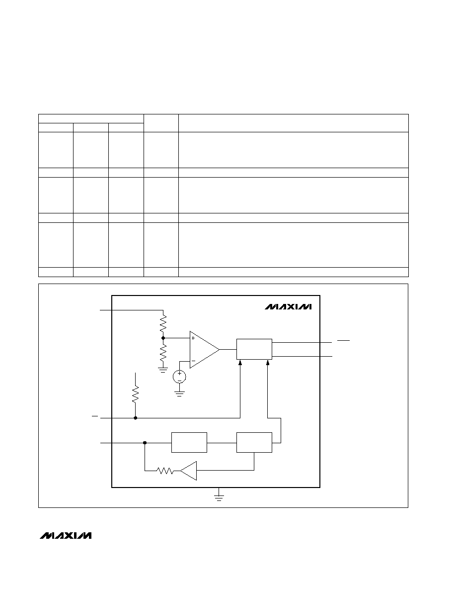
______________________________________________________________Pin Description
MAX823
MAX824
MAX825
V
CC
V
CC
WDI
(MAX823/MAX824
ONLY)
1.25V
GND
RESET
(MAX824/MAX825
ONLY)
RESET
MR
(MAX823/MAX825
ONLY)
RESET
GENERATOR
WATCHDOG
TIMER
WATCHDOG
TRANSITION
DETECTOR
FUNCTION
1
1
Active-Low Reset Output. Pulses low for 200ms when triggered, and remains
low whenever V
CC
is below the reset threshold or when MR is a logic low. It
remains low for 200ms after one of the following occurs: V
CC
rises above the
reset threshold, the watchdog triggers a reset, or MR goes low to high.
2
2
Ground. 0V reference for all signals.
3
--
Manual-Reset Input. A logic low on MR asserts reset. Reset remains asserted as
long as MR is held low and for 200ms after MR returns high. The active-low input
has an internal 52k
pull-up resistor. It can be driven from a CMOS-logic line or
shorted to ground with a switch. Leave open or connect to V
CC
if unused.
--
3
Active-High Reset Output. Inverse of RESET.
5
5
Supply Voltage
4
4
Watchdog Input. If WDI remains either high or low for longer than the watch-
dog timeout period, the internal watchdog timer runs out and a reset is trig-
gered. The internal watchdog timer clears whenever reset is asserted, or
whenever WDI sees a rising or falling edge. If WDI is left unconnected or is
connected to a three-stated buffer output, the watchdog feature is disabled.
NAME
1
RESET
2
GND
4
MR
3
RESET
5
V
CC
--
WDI
Figure 1. Functional Diagram
MAX824
MAX823
MAX825
PIN