_______________General Description
The MAX782 is a system-engineered power-supply con-
troller for notebook computers or similar battery-powered
equipment. It provides two high-performance step-down
(buck) pulse-width modulators (PWMs) for +3.3V and +5V,
and dual PCMCIA VPP outputs powered by an integral fly-
back winding controller. Other functions include dual, low-
dropout, micropower linear regulators for CMOS/RTC back-
up, and three precision low-battery-detection comparators.
High efficiency (95% at 2A; greater than 80% at loads
from 5mA to 3A) is achieved through synchronous recti-
fication and PWM operation at heavy loads, and Idle-
Mode
TM
operation at light loads. It uses physically
small components, thanks to high operating frequen-
cies (300kHz/200kHz) and a new current-mode PWM
architecture that allows for output filter capacitors as
small as 30µF per ampere of load. Line- and load-tran-
sient response are terrific, with a high 60kHz unity-gain
crossover frequency allowing output transients to be
corrected within four or five clock cycles. Low system
cost is achieved through a high level of integration and
the use of low-cost, external N-channel MOSFETs. The
integral flyback winding controller provides a low-cost,
+15V high-side output that regulates even in the
absence of a load on the main output.
Other features include low-noise, fixed-frequency PWM
operation at moderate to heavy loads and a synchroniz-
able oscillator for noise-sensitive applications such as
electromagnetic pen-based systems and communicat-
ing computers. The MAX782 is a monolithic BiCMOS IC
available in fine-pitch, SSOP surface-mount packages.
_______________________Applications
Notebook Computers
Portable Data Terminals
Communicating Computers
Pen-Entry Systems
___________________________Features
o
Dual PWM Buck Controllers (+3.3V and +5V)
o
Dual PCMCIA VPP Outputs (0V/5V/12V)
o
Three Precision Comparators or Level Translators
o
95% Efficiency
o
420µA Quiescent Current;
70µA in Standby (linear regulators alive)
o
5.5V to 30V Input Range
o
Small SSOP Package
o
Fixed Output Voltages Available:
3.3 (standard)
3.45 (High-Speed PentiumTM)
3.6 (PowerPCTM)
______________Ordering Information
MAX782
Triple-Output Power-Supply
Controller for Notebook Computers
________________________________________________________________
Maxim Integrated Products
1
36
35
34
33
32
31
30
29
28
27
26
25
24
23
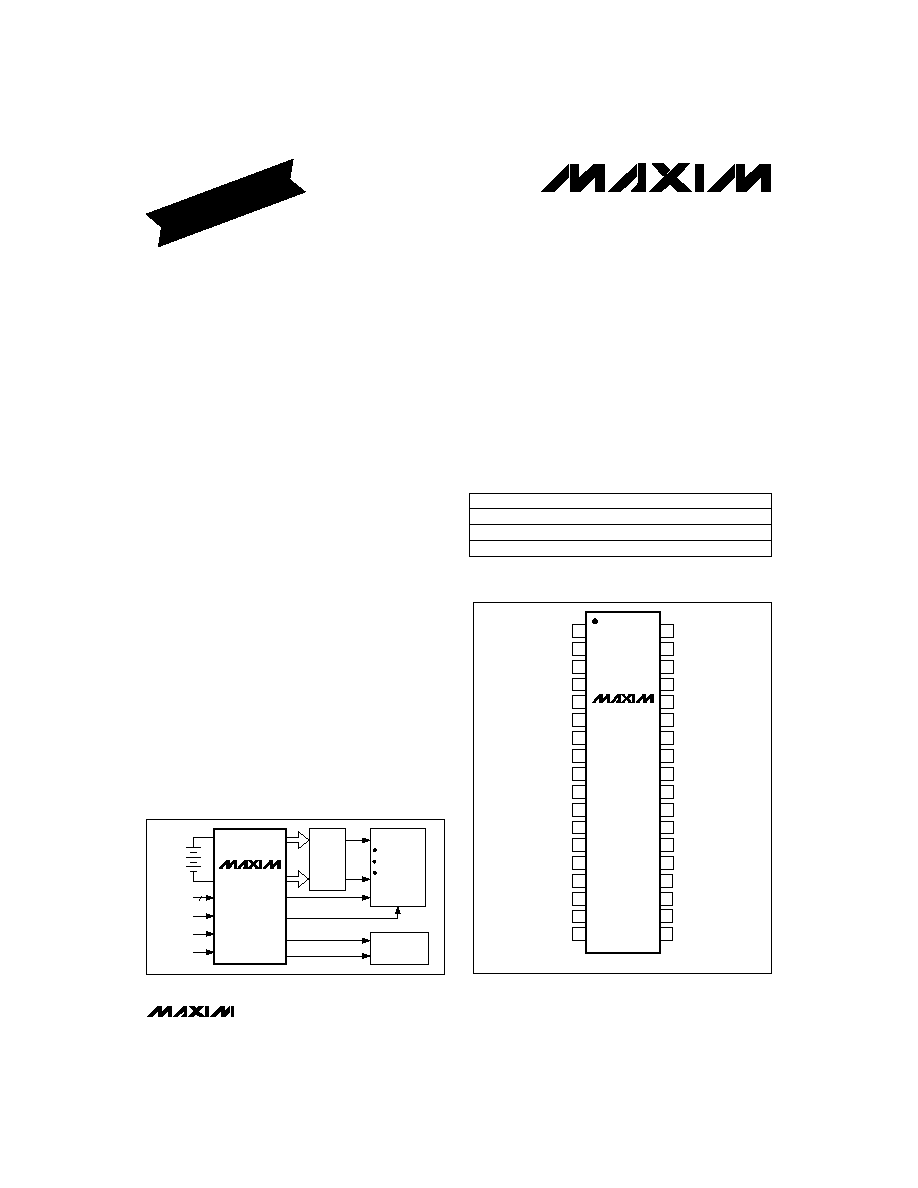
1
2
3
4
5
6
7
8
9
10
11
12
13
14
SS3
CS3
FB3
DH3
LX3
BST3
LX5
DL3
V+
VL
FB5
PGND
DL5
BST5
SYNC
REF
GND
VPPB
VDD
VPPA
Q1
Q2
Q3
VH
D3
D2
D1
ON3
SSOP
TOP VIEW
MAX782
22
21
20
19
15
16
17
18
ON5
DH5
CS5
SS5
DB0
DB1
DA0
DA1
__________________Pin Configuration
MAX782
5.5V
TO
30V
VPP
CONTROL
ON3
ON5
SYNC
POWER
SECTION
SUSPEND POWER
LOW-BATTERY WARNING
VPP (0V/5V/12V)
µ
P
MEMORY
PERIPHERALS
+3.3V
+5V
DUAL
PCMCIA
SLOTS
4
VPP (0V/5V/12V)
______Typical Application Diagram
Call toll free 1-800-998-8800 for free samples or literature.
19-0146; Rev 2; 5/94
PART
TEMP. RANGE
PIN-PACKAGE
MAX782CBX
0°C to +70°C
36 SSOP
MAX782RCBX
0°C to +70°C
36 SSOP
MAX782SCBX
0°C to +70°C
36 SSOP
TM
Idle-Mode is a trademark of Maxim Integrated Products. Pentium is a trademark of Intel. PowerPC is a trademark of IBM.
Evaluation Kit
Information Included
Ordering Information continued on last page.
V
OUT
3.3V
3.45V
3.6V

MAX782
Triple-Output Power-Supply
Controller for Notebook Computers
2
_______________________________________________________________________________________
V+ to GND .................................................................-0.3V, +36V
PGND to GND........................................................................±2V
VL to GND ...................................................................-0.3V, +7V
BST3, BST5 to GND ..................................................-0.3V, +36V
LX3 to BST3.................................................................-7V, +0.3V
LX5 to BST5.................................................................-7V, +0.3V
Inputs/Outputs to GND
(D1-D3, ON5, REF, SYNC, DA1, DA0, DB1, DB0, ON5,
SS5, CS5, FB5, CS3, FB3, SS3, ON3) ..........-0.3V, (VL + 0.3V)
VDD to GND.................................................................-0.3V, 20V
VPPA, VPPB to GND.....................................-0.3V, (VDD + 0.3V)
VH to GND ...................................................................-0.3V, 20V
Q1-Q3 to GND.................................................-0.3V, (VH + 0.3V)
DL3, DL5 to PGND...........................................-0.3V, (VL + 0.3V)
DH3 to LX3 ..................................................-0.3V, (BST3 + 0.3V)
DH5 to LX5 ..................................................-0.3V, (BST5 + 0.3V)
REF, VL, VPP Short to GND........................................Momentary
REF Current.........................................................................20mA
VL Current ...........................................................................50mA
VPPA, VPPB Current .........................................................100mA
Continuous Power Dissipation (T
A
= +70°C)
SSOP (derate 11.76mW/°C above +70°C) ...................941mW
Operating Temperature Ranges:
MAX782CBX/MAX782__CBX ...............................0°C to +70°C
MAX782EBX/MAX782__EBX ............................-40°C to +85°C
Storage Temperature Range .............................-65°C to +160°C
Lead Temperature (soldering, 10sec) .............................+300°C
ELECTRICAL CHARACTERISTICS
(V+ = 15V, GND = PGND = 0V, I
VL
= I
REF
= 0mA, ON3 = ON5 = 5V, other digital input levels are 0V or +5V, T
A
= T
MIN
to T
MAX
,
unless otherwise noted.)
Stresses beyond those listed under "Absolute Maximum Ratings`" may cause permanent damage to the device. These are stress ratings only, and functional
operation of the device at these or any other conditions beyond those indicated in the operational sections of the specifications is not implied. Exposure to
absolute maximum rating conditions for extended periods may affect device reliability.
ABSOLUTE MAXIMUM RATINGS
V
MAX782S
MAX782R
MAX782
FB3 Output Voltage
3.46
3.65
3.75
0mV < (CS3-FB3) < 70mV, 6V < V+ < 30V
(includes load and line regulation)
3.32
3.50
3.60
PARAMETER
CONDITIONS
MIN
TYP
MAX
UNITS
Current-Limit Voltage
CS5-FB5 (VDD < 13V, flyback mode)
-50
-100
-160
mV
CS3-FB3 or CS5-FB5
Line Regulation
Either controller (V+ = 6V to 30V)
0.03
%/V
Load Regulation
Either controller (CS_ - FB_ = 0mV to 70mV)
2
%
SS3/SS5 Source Current
2.5
4.0
6.5
µA
SS3/SS5 Fault Sink Current
2
mA
VDD Regulation Setpoint
Falling edge, hysteresis = 1%
V
FB5 Output Voltage
4.80
5.08
5.20
V
3.17
3.35
3.46
Input Supply Range
5.5
30
V
VDD Shunt Setpoint
Rising edge, hysteresis = 1%
V
VDD Shunt Current
VDD = 20V
2
3
mA
Quiescent VDD Current
140
300
µA
VDD Off Current
15
30
µA
Program to 12V, 13V < VDD < 19V, 0mA < I
L
< 60mA
11.6
12.1
12.5
0mV < (CS5-FB5) < 70mV, 6V < V+ < 30V
(includes load and line regulation)
VDD = 18V, ON3 = ON5 = 5V,
VPPA/B programmed to 12V with no external load
Program to 5V, 13V < VDD < 19V, 0mA < I
L
< 60mA
4.85
5.05
5.20
VPPA/VPPB Output Voltage
Program to 0V, 13V < VDD < 19V, -0.3mA < I
L
< 0.3mA
-0.3
0.3
V
VPPA/VPPB Off Input Current
Program to Hi-Z, VDD = 19V, 0V < VPP < 12V
35
µA
VDD = 18V, ON3 = ON5 = 5V,
VPPA/B programmed to Hi-Z or 0V
18
20
13
14
80
100
120
+3.3V AND 5V STEP-DOWN CONTROLLERS
15V FLYBACK CONTROLLER
PCMCIA REGULATORS
(Note 1)
V
V
MAX782
Triple-Output Power-Supply
Controller for Notebook Computers
_______________________________________________________________________________________
3
PARAMETER
CONDITIONS
MIN
TYP
MAX
UNITS
D1-D3 Trip Voltage
Falling edge, hysteresis = 1%
Q1-Q3 Output Low Voltage
VL Output Voltage
REF Fault Lockout Voltage
Falling edge
2.4
3.2
ON5 = ON3 = 0V, 5.5V < V+ < 30V, 0mA < I
L
< 25mA
V
REF Output Voltage
No external load (Note 2)
3.24
3.36
V
4.5
5.5
REF Load Regulation
0mA < I
L
< 5mA
30
75
mV
V+ Standby Current
70
110
µA
1.61
1.69
V
D1-D3 Input Current
D1 = D2 = D3 = 0V to 5V
V
D1 = D2 = D3 = DA0 = DA1 = DB0 = DB1 = 0V,
FB5 = CS5 = 5.25V, FB3 = CS3 = 3.5V
6.0
8.6
±100
mW
V+ Off Current
nA
FB5 = CS5 = 5.25V, VL switched over to FB5
30
60
µA
Q1-Q3 Source Current
VH = 15V, Q1-Q3 forced to 2.5V
12
20
30
µA
Q1-Q3 Sink Current
VL Fault Lockout Voltage
VH = 15V, Q1-Q3 forced to 2.5V
200
500
1000
µA
Q1-Q3 Output High Voltage
I
SOURCE
= 5µA, VH = 3V
VH-0.5
V
I
SINK
= 20µA, VH = 3V
0.4
V
Quiescent VH Current
VH = 18V, D1 = D2 = D3 = 5V, no external load
Falling edge, hysteresis = 1%
3.6
4.2
V
6
10
µA
VL/FB5 Switchover Voltage
Rising edge of FB5, hysteresis = 1%
4.2
4.7
V
Note 1:
Output current is further limited by maximum allowable package power dissipation.
Note 2:
Since the reference uses VL as its supply, V+ line regulation error is insignificant.
ELECTRICAL CHARACTERISTICS (continued)
(V+ = 15V, GND = PGND = 0V, I
VL
= I
REF
= 0mA, ON3 = ON5 = 5V, other digital input levels are 0V or +5V, T
A
= T
MIN
to T
MAX
,
unless otherwise noted.)
Quiescent Power Consumption
(both PWM controllers on)
D1 = D2 = D3 = ON3 = ON5 = DA0 = DA1 = DB0 =
DB1 = 0V, V+ = 30V
SYNC Low Pulse Width
200
ns
SYNC High Pulse Width
200
ns
Oscillator Frequency
SYNC = 0V or 5V
170
200
230
kHz
SYNC = 3.3V
270
300
330
Maximum Duty Cycle
SYNC = 0V or 5V
92
95
%
SYNC = 3.3V
89
92
Oscillator SYNC Range
240
350
kHz
SYNC Rise/Fall Time
Not tested
200
ns
Input Low Voltage
ON3, ON5, DA0, DA1, DB0, DB1, SYNC
0.8
V
ON3, ON5, DA0, DA1, DB0, DB1
2.4
Input Current
ON3, ON5, DA0, DA1, DB0, DB1, V
IN
= 0V or 5V
±1
µA
DL3/DL5 Sink/Source Current
DL3, DL5 forced to 2V
1
A
DL3/DL5 On Resistance
High or low
7
DH3/DH5 On Resistance
High or low, BST3-LX3 = BST5-LX5 = 4.5V
7
Input High Voltage
SYNC
VL-0.5
V
DH3/DH5 Sink/Source Current
BST3-LX3 = BST5-LX5 = 4.5V, DH3, DH5 forced to 2V
1
A
INTERNAL REGULATOR AND REFERENCE
COMPARATORS
OSCILLATOR AND INPUTS/OUTPUTS
MAX782
Triple-Output Power-Supply
Controller for Notebook Computers
4
_______________________________________________________________________________________
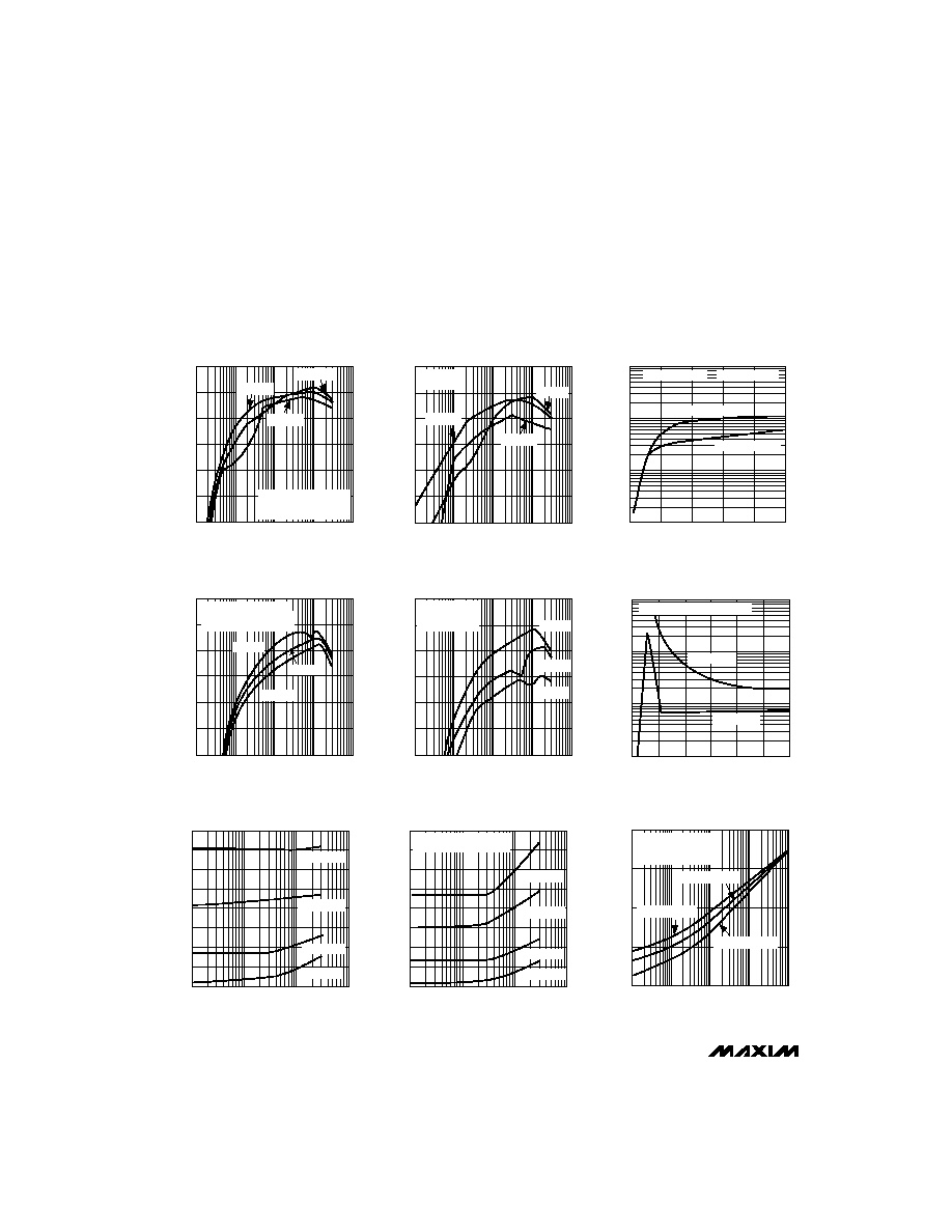
__________________________________________Typical Operating Characteristics
(Circuit of Figure 1, Transpower transformer type TTI5870, T
A
= +25°C, unless otherwise noted.)
100
70
0.001
0.1
10
EFFICIENCY vs.
+3.3V OUTPUT CURRENT, 200kHz
80
+3.3V OUTPUT CURRENT (A)
EFFICIENCY (%)
90
+5V ON, +5V LOAD = 0mA
I
DD
= 0mA,
COMPONENTS OF TABLE 5
V
IN
= 6V
V
IN
= 10V
V
IN
= 15V
0.01
1
10
0.01
5
10
20
30
I
DD
OUTPUT CURRENT vs. INPUT VOLTAGE
COILTRONIX CTX03-12062 TRANSFORMER
0.1
1
INPUT VOLTAGE (V)
I
DD
LOAD CURRENT (A)
15
25
+3V LOAD = 0mA
R
SENSE
= 0.020
+5V LOAD = 0A-1A
+5V LOAD = 3A
100
70
0.001
0.1
10
EFFICIENCY vs.
+5V OUTPUT CURRENT, 200kHz
80
+5V OUTPUT CURRENT (A)
EFFICIENCY (%)
90
0.01
1
V
IN
= 6V
V
IN
= 15V
V
IN
= 10V
COMPONENTS,
OF TABLE 5. SYNC = 0V,
+3.3V OFF, I
DD
= 0mA
10000
10
0
5
15
25
QUIESCENT INPUT CURRENT vs.
INPUT VOLTAGE
100
1000
INPUT VOLTAGE (V)
INPUT CURRENT (
µ
A)
10
20
30
+3.3V LOAD = +5V LOAD = 0mA
+5V, +3V ON
+5V, +3V OFF
100
70
0.001
0.01
1
EFFICIENCY vs.
+5V OUTPUT CURRENT, 300kHz
80
90
+5V OUTPUT CURRENT (A)
EFFICIENCY (%)
0.1
10
I
DD
= 0mA
+3.3V OFF
V
IN
= 30V
V
IN
= 15V
V
IN
= 6V
100
70
0.001
0.01
1
EFFICIENCY vs.
+3.3V OUTPUT CURRENT, 300kHz
80
90
+3.3V OUTPUT CURRENT (A)
EFFICIENCY (%)
0.1
10
V
IN
= 30V
V
IN
= 15V
V
IN
= 6V
I
DD
= 0mA
+5V ON
+5V LOAD = 0mA
8
5
0.01
0.1
10
+5V OUTPUT CURRENT vs.
MINIMUM INPUT VOLTAGE, 200kHz
6
7
+5V LOAD CURRENT (A)
MINIMUM INPUT VOLTAGE (V)
1
9
COMPONENTS OF TABLE 4,
SYNC = 0V
I
DD
= 0mA
I
DD
= 60mA
I
DD
= 140mA
I
DD
= 300mA
9
5
0.01
0.1
10
+5V OUTPUT CURRENT vs.
MINIMUM INPUT VOLTAGE, 300kHz
6
7
+5V OUTPUT CURRENT (A)
MINIMUM INPUT VOLTAGE (V)
1
8
I
DD
= 300mA
I
DD
= 140mA
I
DD
= 60mA
I
DD
= 0mA
1000
0.1
100
µ
A
10mA
1A
SWITCHING FREQUENCY vs.
LOAD CURRENT
10
LOAD CURRENT
SWITCHING FREQUENCY (kHz)
100
1mA
100mA
CIRCUIT OF FIGURE 1,
SYNC = REF (300kHz)
ON3 = ON5 = 5V
+5V, V
IN
= 7.5V
1
+5V, V
IN
= 30V
+3.3V, V
IN
= 7.5V

MAX782
Triple-Output Power-Supply
Controller for Notebook Computers
_______________________________________________________________________________________
5
HORIZONTAL = 500ns/div
+5V OUTPUT CURRENT = 1A
INPUT VOLTAGE = 16V
PULSE-WIDTH MODULATION MODE WAVEFORMS
LX VOLTAGE
10V/div
+5V OUTPUT
VOLTAGE
50mV/div
_____________________________Typical Operating Characteristics (continued)
(Circuit of Figure 1, Transpower transformer type TTI5870, T
A
= +25°C, unless otherwise noted.)
HORIZONTAL = 5
µ
s/div
+5V OUTPUT CURRENT = 42mA
INPUT VOLTAGE = 16V
IDLE-MODE WAVEFORMS
LX VOLTAGE
10V/div
+5V OUTPUT
VOLTAGE
50mV/div
HORIZONTAL = 200
µ
s/div
V
IN
= 15V
+3.3V LOAD-TRANSIENT RESPONSE
+3.3V OUTPUT
50mV/div
3A
0A
LOAD CURRENT
HORIZONTAL = 200
µ
s/div
V
IN
= 15V
+5V LOAD-TRANSIENT RESPONSE
+5V OUTPUT
50mV/div
3A
0A
LOAD CURRENT