
_______________General Description
The MAX770MAX773 step-up switching controllers pro-
vide 90% efficiency over a 10mA to 1A load. A
unique current-limited pulse-frequency-modulation (PFM)
control scheme gives these devices the benefits of
pulse-width-modulation (PWM) converters (high efficiency
at heavy loads), while using less than 110µA of supply
current (vs. 2mA to 10mA for PWM converters).
These ICs use tiny external components. Their high
switching frequencies (up to 300kHz) allow surface-
mount magnetics of 5mm height and 9mm diameter.
The MAX770/MAX771/MAX772 accept input voltages
from 2V to 16.5V. Output voltages are preset at 5V,
(MAX770), 12V (MAX771), and 15V (MAX772); they can
also be adjusted using two resistors.
The MAX773 accepts inputs from 3V to 16.5V. For a wider
input range, it features an internal shunt regulator that
allows unlimited higher input voltages. The MAX773's out-
put can be set to 5V, 12V, or 15V, or it can be adjusted
with two resistors.
The MAX770MAX773 drive external N-channel MOSFET
switches, allowing them to power loads up to 15W. If less
power is required, use the MAX756/MAX757 or
MAX761/MAX762 step-up switching regulators with on-
board MOSFETs.
________________________Applications
Palmtops/Handy-Terminals
High-Efficiency DC-DC Converters
Battery-Powered Applications
Positive LCD-Bias Generators
Portable Communicators
Flash Memory Programmers
____________________________Features
o
90% Efficiency for 10mA to 1A Load Currents
o
Up to 15W Output Power
o
110µA Max Supply Current
o
5µA Max Shutdown Current
o
2V to 16.5V Input Range
(MAX770/MAX771/MAX772)
o
Internal Shunt Regulator for High Input Voltages
(MAX773)
o
Preset or Adjustable Output Voltages
MAX770: 5V or Adjustable
MAX771: 12V or Adjustable
MAX772: 15V or Adjustable
MAX773: 5V, 12V, 15V, or Adjustable
o
Current-Limited PFM Control Scheme
o
300kHz Switching Frequency
______________Ordering Information
Ordering Information continued at end of data sheet.
*Contact factory for dice specifications.
**Contact factory for availability and processing to MIL-STD-883B.
MAX770MAX773
5V/12V/15V or Adjustable, High-Efficiency,
Low I
Q
, Step-Up DC-DC Controllers
________________________________________________________________
Maxim Integrated Products
1
1
2
3
4
8
7
6
5
CS
GND
AGND
REF
SHDN
FB
V+
EXT
MAX770
MAX771
MAX772
DIP/SO
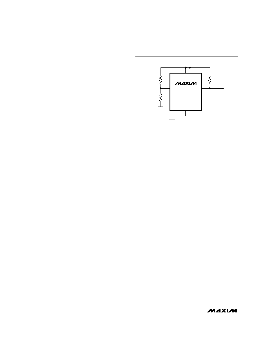
_________________Pin Configurations
FB AGND GND
V+
CS
EXT
N
REF
SHDN
ON/OFF
OUTPUT
12V
INPUT
2V TO VOUT
MAX771
__________Typical Operating Circuit
PART
TEMP. RANGE
PIN-PACKAGE
MAX770
CPA
0°C to +70°C
Plastic DIP
MAX770CSA
0°C to +70°C
8 SO
MAX770C/D
0°C to +70°C
Dice*
MAX770EPA
-40°C to +85°C
8 Plastic DIP
MAX770ESA
-40°C to +85°C
8 SO
MAX770MJA
-55°C to +125°C
8 CERDIP**
TOP VIEW
Pin Configurations continued at end of data sheet.
19-0202; Rev 2; 11/96
EVALUATION KIT MANUAL
FOLLOWS DATA SHEET
For free samples & the latest literature: http://www.maxim-ic.com, or phone 1-800-998-8800.
For small orders, phone 408-737-7600 ext. 3468.

MAX770MAX773
5V/12V/15V or Adjustable, High-Efficiency,
Low I
Q
, Step-Up DC-DC Controllers
2
_______________________________________________________________________________________
ABSOLUTE MAXIMUM RATINGS
Supply Voltages
V+ to GND.............................................................-0.3V to 17V
V+ to SGND.............................................................-0.3V to 7V
SGND........................................................-0.3V to (V+ + 0.3V)
EXT, CS, REF, LBO, LBI, SHDN, FB.............-0.3V to (V+ + 0.3V)
EXTH, EXTL ..................................................-0.3V to (V+ + 0.3V)
V5, V12, V15 .............................................................-0.3V to 17V
GND to AGND .........................................................0.1V to -0.1V
I
SGND
..................................................................................50mA
Continuous Power Dissipation (T
A
= +70°C)
8-Pin Plastic DIP (derate 9.09mW/°C above +70°C)....727mW
8-Pin SO (derate 5.88mW/°C above +70°C) ................471mW
8-Pin CERDIP (derate 8.00mW/°C above +70°C) ........640mW
14-Pin Plastic DIP
(derate 10.00mW/°C above +70°C) .............................800mW
14-Pin SO (derate 8.33mW/°C above +70°C) ..............667mW
14-Pin CERDIP (derate 9.09mW/°C above +70°C) ......727mW
Operating Temperature Ranges
MAX77_C_ _ ........................................................0°C to +70°C
MAX77_E_ _......................................................-40°C to +85°C
MAX77_MJ_ ...................................................-55°C to +125°C
Junction Temperatures
MAX77_C_ _/E_ _ ..........................................................+150°C
MAX77_MJ_..................................................................+175°C
Storage Temperature Range .............................-65°C to +160°C
Lead Temperature (soldering, 10sec) .............................+300°C
Stresses beyond those listed under "Absolute Maximum Ratings" may cause permanent damage to the device. These are stress ratings only, and functional
operation of the device at these or any other conditions beyond those indicated in the operational sections of the specifications is not implied. Exposure to
absolute maximum rating conditions for extended periods may affect device reliability.
ELECTRICAL CHARACTERISTICS
(V+ = 5V, I
LOAD
= 0mA, T
A
= T
MIN
to T
MAX
, unless otherwise noted. Typical values are at T
A
= +25°C.)
PARAMETER
SYMBOL
CONDITIONS
MIN
TYP
MAX
UNITS
Supply Current
85
110
µ
A
Standby Current
2
5
µ
A
4
Output Voltage (Note 1)
V+ = 2.0V to 5.0V, over full load range
4.80
5.0
5.20
V
V+ = 2.0V to 12.0V, over full load range
11.52
12.0
12.48
V+ = 2.0V to 15.0V, over full load range
14.40
15.0
15.60
Figure 2a, V+ = 2.7V to 4.5V,
I
LOAD
= 700mA, V
OUT
= 5V
5
mV/V
Figure 2a, V+ = 3V, I
LOAD
= 30mA to 1A,
V
OUT
= 5V
20
mV/A
Maximum Switch On-Time
t
ON
(max)
12
16
20
µ
s
Minimum Switch Off-Time
t
OFF
(min)
1.8
2.3
2.8
µ
s
Efficiency
87
%
Reference Voltage
V
REF
I
REF =
0
µ
A
MAX77_C
1.4700
1.5
1.5300
V
MAX77_E
1.4625
1.5
1.5375
MAX77_M
1.4550
1.5
1.5450
Output Voltage Line Regulation
(Note 2)
Output Voltage Load Regulation
(Note 2)
V+ = 4V, I
LOAD
= 500mA, V
OUT
= 5V
V+ = 10.0V, SHDN
1.6V (shutdown)
V+ = 16.5V, SHDN
1.6V (shutdown)
V+ = 16.5V, SHDN = 0V (normal operation)
Minimum Start-Up Voltage
MAX770/MAX771/MAX772
1.8
2.0
V
MAX770772 (internal feedback resistors)
2.0
16.5
MAX770772C/E (external resistors)
3.0
16.5
MAX770772MJA (external resistors)
3.1
16.5
MAX773C/E
3.0
16.5
MAX773MJD
3.1
16.5
Input Voltage Range
V

MAX770MAX773
5V/12V/15V or Adjustable, High-Efficiency,
Low I
Q
, Step-Up DC-DC Controllers
_______________________________________________________________________________________
3
ELECTRICAL CHARACTERISTICS (continued)
(V+ = 5V, I
LOAD
= 0mA, T
A
= T
MIN
to T
MAX
, unless otherwise noted. Typical values are at T
A
= +25°C.)
PARAMETERS
SYMBOL
CONDITIONS
MIN
TYP
MAX
UNITS
REF Load Regulation
0
µ
A
I
REF
100
µ
A
MAX77_C/E
4
10
mV
MAX77_M
4
15
REF Line Regulation
3V
V+
16.5V
40
100
µ
V/V
FB Trip-Point Voltage
V
FB
MAX77_C
1.4700
1.50
1.5300
V
MAX77_E
1.4625
1.50
1.5375
MAX77_M
1.4550
1.50
1.5450
FB Input Current
I
FB
MAX77_C
±20
nA
MAX77_E
±40
MAX77_M
±60
SHDN Input High Voltage
V
IH
V+ = 2.0V to 16.5V
1.6
V
SHDN Input Low Voltage
V
IL
MAX77_C/E, V+ = 2.0V to 16.5V
0.4
V
SHDN Input Current
±1
µ
A
LBI Input Current
MAX773, V+ = 16.5V, LBI = 1.5V
±20
nA
LBI Hysteresis
MAX773
20
LBI Threshold Voltage
MAX773, LBI falling
MAX77_C
1.4700
1.50
1.5300
V
MAX77_E
1.4625
1.50
1.5375
MAX77_M
1.4550
1.50
1.5450
LBO Leakage Current
MAX773, V+ = 16.5V, V
LBO
= 16.5V
0.01
1.00
µ
A
LBO Output Voltage Low
V
OL
MAX773, V+ = 5V, LBO sinking 1mA
0.1
0.4
V
V+ = 16.5V, SHDN = 0V or V+
mV
Current-Limit Trip Level
V
CS
V+ = 5V to 16.5V
170
200
230
mV
V
SHUNT
MAX773, I
SHUNT
= 1mA to 20mA,
SGND = 0V, C
SHUNT
= 0.1
µ
F
5.5
6.3
V
CS Input Current
0.01
±1
µ
A
EXT Rise Time
V+ = 5V, 1nF from EXT to ground (Note 3)
55
ns
EXT Fall Time
V+ = 5V, 1nF from EXT to ground (Note 3)
55
ns
Supply Voltage in
Shunt Mode
Note 1:
Output voltage guaranteed using preset voltages. See Figures 7a7d for output current capability versus input voltage.
Note 2:
Output voltage line and load regulation depend on external circuit components.
Note 3:
For the MAX773, EXT is EXTH and EXTL shorted together.
LBI Delay
5mV overdrive
2.5
µs
MAX77_M, V+ = 2.0V to 16.5V
0.2
0
1
2
3
4
-75
-50
-25
0
25
50
75
100 125
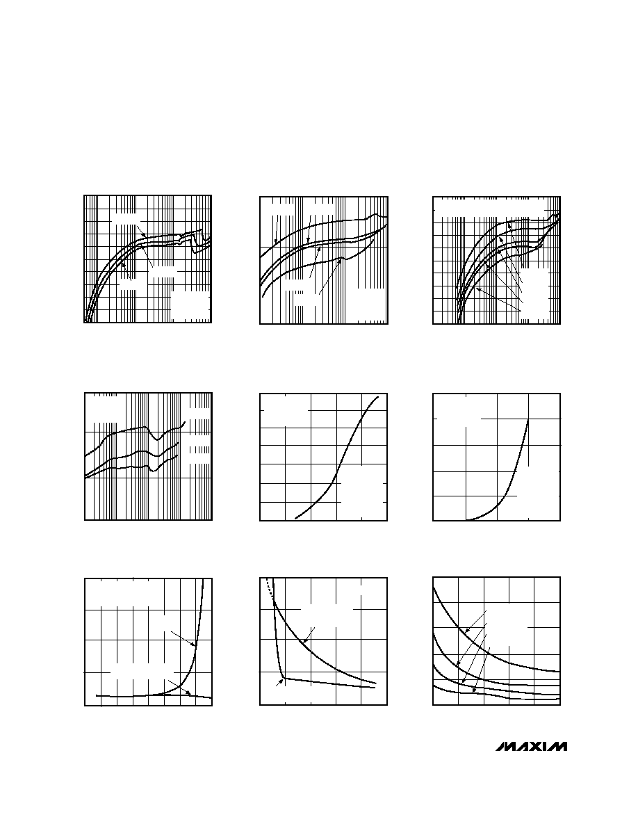
SUPPLY CURRENT vs. TEMPERATURE
TEMPERATURE (°C)
SUPPLY CURRENT (mA)
V
OUT
= 12V, V
IN
= 5V
CIRCUIT OF FIGURE 2b
BOOTSTRAPPED MODE
ENTIRE
CIRCUIT
SCHOTTKY DIODE
LEAKAGE EXCLUDED
MAX7703-07
0
0.2
0.4
0.6
0.8
2
4
6
8
10
12
SUPPLY CURRENT vs. SUPPLY VOLTAGE
SUPPLY VOLTAGE (V)
SUPPLY CURRENT (mA)
V
OUT
= 12V
NON-BOOTSTRAPPED
CIRCUIT OF FIGURE 2c
BOOTSTRAPPED
CIRCUIT OF
FIGURE 2b
MAX7703-08
0
100
150
200
250
50
2
4
6
8
10
12
EXT RISE/FALL TIME vs. SUPPLY VOLTAGE
V+ (V)
EXT RISE/FALL TIME (ns)
C
EXT
= 2200pF
C
EXT
= 1000pF
C
EXT
= 446pF
C
EXT
= 100pF
MAX7703-09
100
50
0.001
0.01
0.1
1
MAX772
EFFICIENCY vs. OUTPUT CURRENT
(BOOTSTRAPPED)
60
OUTPUT CURRENT (A)
EFFICIENCY (%)
70
80
90
V
OUT
= 15V, CIRCUIT OF FIGURE 2b
MAX772 SUBSTITUTED FOR MAX771
V
IN
= 12V
V
IN
= 9V
V
IN
= 6V
V
IN
= 5V
V
IN
= 3V
MAX7703-03
50
60
70
80
90
100
0.001
0.01
1
MAX771
EFFICIENCY vs. OUTPUT CURRENT
(BOOTSTRAPPED)
OUTPUT CURRENT (A)
EFFICIENCY (%)
0.1
V
IN
= 6V
V
IN
= 5V
V
IN
= 3V
V
IN
= 9V
V
OUT
= 12V
CIRCUIT OF
FIGURE 2b
MAX7703-02
100
50
0.001
0.01
0.1
1
MAX770
EFFICIENCY vs. OUTPUT CURRENT
(BOOTSTRAPPED)
60
OUTPUT CURRENT (A)
EFFICIENCY (%)
70
80
90
V
IN
= 3V
V
IN
= 3.5V
V
OUT
= 5V
CIRCUIT OF
FIGURE 2a
V
IN
= 4V
MAX7703-01
MAX770MAX773
5V/12V/15V or Adjustable, High-Efficiency,
Low I
Q
, Step-Up DC-DC Controllers
4
_______________________________________________________________________________________
__________________________________________Typical Operating Characteristics
(T
A
= +25°C, unless otherwise noted.)
70
80
90
100
0.001
0.01
0.1
10
1
MAX771
EFFICIENCY vs. OUTPUT CURRENT
(NON-BOOTSTRAPPED)
OUTPUT CURRENT (A)
EFFICIENCY (
%
)
V
IN
= 9V
V
IN
= 6V
V
IN
= 5V
V
OUT
= 12V
CIRCUIT OF
FIGURE 2c
MAX7703-04
0
100
200
300
400
500
600
700
1.0
MAX770
LOAD CURRENT vs.
MINIMUM START-UP INPUT VOLTAGE
MINIMUM START-UP INPUT VOLTAGE (V)
LOAD CURRENT (mA)
3.0
1.5
2.5
3.5
2.0
ABOVE 3.4V,
THE CIRCUIT
STARTS UP
UNDER
MAXIMUM
LOAD
CONDITIONS
V
OUT
= 5V
CIRCUIT OF
FIGURE 2a
MAX7703-05
0
100
200
300
400
500
2.0
MAX771
LOAD CURRENT vs.
MINIMUM START-UP INPUT VOLTAGE
MINIMUM START-UP INPUT VOLTAGE (V)
LOAD CURRENT (mA)
4.0
2.5
3.5
3.0
ABOVE 3.5V
THE CIRCUIT
STARTS UP
UNDER
MAXIMUM
LOAD
CONDITIONS
V
OUT
= 12V
CIRCUIT OF
FIGURE 2b
MAX7703-06
MAX770MAX773
5V/12V/15V or Adjustable, High-Efficiency,
Low I
Q
, Step-Up DC-DC Controllers
_______________________________________________________________________________________
5
250
0
-60
-20
60
140
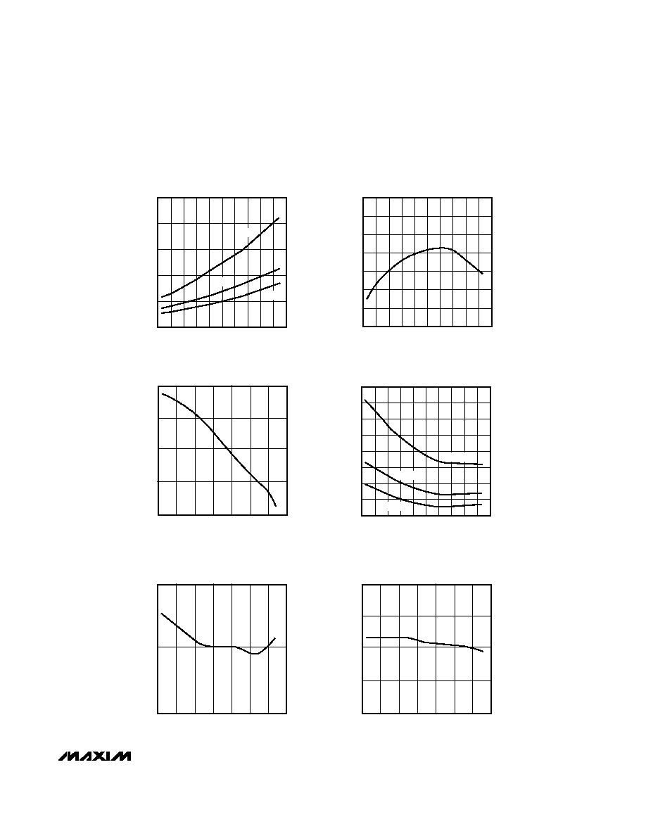
REFERENCE OUTPUT RESISTANCE vs.
TEMPERATURE
50
MAX7703-10
TEMPERATURE (
°
C)
REFERENCE OUTPUT RESISTANCE (
)
20
100
150
-40
0
80
40
120
100
200
100µA
50µA
10µA
1.502
-60
-20
60
140
REFERENCE vs. TEMPERATURE
MAX7703-11
TEMPERATURE (
°
C)
REFERENCE (V)
20
100
-40
0
80
40
120
1.500
1.498
1.496
1.494
1.492
1.504
1.506
4.0
-60
-20
60
140
SHUTDOWN CURRENT vs. TEMPERATURE
MAX7703-12
TEMPERATURE (
°
C)
I
CC
(µA)
20
100
-40
0
80
40
120
3.5
3.0
2.5
2.0
1.5
1.0
0.5
0
V+ = 15V
V+ = 4V
V+ = 8V
15.5
16.0
16.5
-60 -30
0
30
60
90
120
150
MAXIMUM SWITCH ON-TIME vs.
TEMPERATURE
TEMPERATURE (°C)
t ON(MAX) (µs)
MAX7703-13
2.20
2.25
2.30
-60 -30
0
30
60
90
120
150
MINIMUM SWITCH OFF-TIME vs.
TEMPERATURE
TEMPERATURE (°C)
t OFF(MIN) (µs)
MAX7703-14
6.0
7.0
8.0
-60 -30
0
30
60
90
120
150
MAXIMUM SWITCH ON-TIME/
MINIMUM SWITCH OFF-TIME RATIO
vs. TEMPERATURE
TEMPERATURE (°C)
t ON(MAX)/
t OFF(MIN) RATIO
MAX7703-15
7.5
6.5
____________________________Typical Operating Characteristics (continued)
(T
A
= +25°C, unless otherwise noted.)
MAX770MAX773
5V/12V/15V or Adjustable, High-Efficiency,
Low I
Q
, Step-Up DC-DC Controllers
6
_______________________________________________________________________________________
V
IN
= 2.9V, I
OUT
= 0.9A
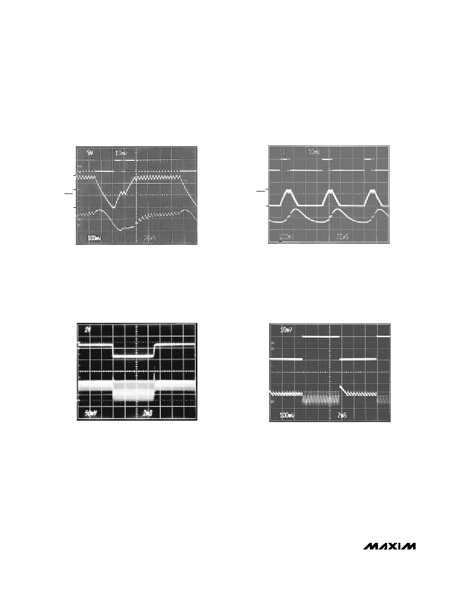
A: EXT VOLTAGE, 5V/div
B: INDUCTOR CURRENT 1A/div
C: V
OUT
RIPPLE 100mV/div, AC-COUPLED
MAX770
HEAVY-LOAD SWITCHNG WAVEFORMS
20
µ
s/div
V
OUT
0
A
I
LIM
I
LIM
2
B
C
0
V+ = 3V, I
OUT
= 165mA
A: EXT VOLTAGE, 5V/div
B: INDUCTOR CURRENT, 1A/div
C: V
OUT
RIPPLE 100mV/div, AC-COUPLED
MAX770
LIGHT-LOAD SWITCHING WAVEFORMS
20
µ
s/div
0
B
A
C
ILIM
2
I
OUT
= 0.7A
A: V
IN
, 2.7V TO 4.5V, 2V/div
B: V
OUT
RIPPLE, 100mV/div, AC-COUPLED
MAX770
LINE-TRANSIENT RESPONSE
A
B
4.5V
2.7V
0
2ms/div
V
IN
= 3V
A: LOAD CURRENT 0.5A/div (0A to 1A)
B: V
OUT
RIPPLE, 100mV/div, AC-COUPLED
MAX770
LOAD-TRANSIENT RESPONSE
2ms/div
A
B
0
____________________________Typical Operating Characteristics (continued)
(Circuit of Figure 2a, T
A
= +25°C, unless otherwise noted.)

MAX770MAX773
5V/12V/15V or Adjustable, High-Efficiency,
Low I
Q
, Step-Up DC-DC Controllers
_______________________________________________________________________________________
7
V
IN
= 3V, I
OUT
= 0.5A
A: SHDN, 2V/div
B: V
OUT
, 2V/div
MAX770
EXITING SHUTDOWN
A
B
0
0
200
µ
s/div
______________________________________________________________Pin Description
____________________________Typical Operating Characteristics (continued)
(Circuit of Figure 2a, T
A
= +25°C, unless otherwise noted.)
PIN
NAME
FUNCTION
MAX773
1
--
EXT
Gate drive for external N-channel power transistor
2
3
V+
3
6
FB
4
7
SHDN
5
8
REF
6
--
AGND
Analog ground
7
9
GND
High-current ground return for the output driver
8
11
CS
--
1
V12
--
2
V5
MAX770
MAX771
MAX772
Power-supply input. Also acts as a voltage-sense point when in bootstrapped mode for the
MAX770/MAX771/MAX772, or as a shunt regulator when SGND is connected to ground for the
MAX773. Bypass to SGND with 0.1
µ
F when using the shunt regulator.
Feedback input for adjustable-output operation. Connect to ground for fixed-output operation. Use
a resistor divider network to adjust the output voltage. See
Setting the Output Voltage section.
Active-high TTL/CMOS logic-level shutdown input. In shutdown mode, V
OUT
is a diode drop
below V+ (due to the DC path from V+ to the output) and the supply current drops to 5
µ
A
maximum. Connect to ground for normal operation.
1.5V reference output that can source 100
µ
A for external loads. Bypass to GND with 0.1
µ
F.
The reference is disabled in shutdown.
Positive input to the current-sense amplifier. Connect the current-sense resistor between CS and GND.
Input sense point for 12V-output operation. Connect V
OUT
to V12 for 12V-output operation.
Leave unconnected for adjustable-output operation.
Input sense point for 5V-output operation. Connect V
OUT
to V5 for 5V-output operation. Leave
unconnected for adjustable-output operation.
--
4
LBO
--
5
LBI
Input to the internal low-battery comparator. Tie to GND or V+ if not used.
--
10
SGND
Shunt regulator ground. Leave unconnected if the shunt regulator is
not
used.
Low-battery output is an open-drain output that goes low when LBI is less than 1.5V. Connect to V+
through a pull-up resistor. Leave floating if not used. LBO is high impedance in shutdown mode.

MAX770MAX773
5V/12V/15V or Adjustable, High-Efficiency,
Low I
Q
, Step-Up DC-DC Controllers
8
_______________________________________________________________________________________
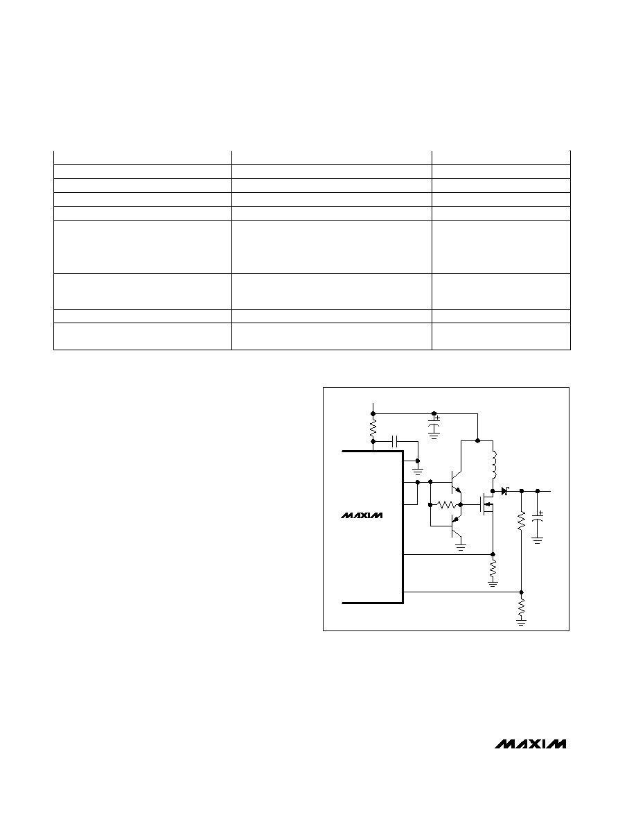
_______________Detailed Description
The MAX770MAX773 are BiCMOS, step-up, switch-
mode power-supply controllers that provide preset 5V,
12V, and 15V output voltages, in addition to adjustable-
output operation. Their unique control scheme com-
bines the advantages of pulse-frequency modulation
(low supply current) and pulse-width modulation (high
efficiency with heavy loads), providing high efficiency
over a wide output current range, as well as increased
output current capability over previous PFM devices.
In addition, the external sense resistor and power
transistor allow the user to tailor the output current
capability for each application. Figure 1 shows the
MAX770MAX773 block diagram.
The MAX770MAX773 offer three main improvements
over prior pulse-skipping control solutions: 1) the con-
verters operate with tiny (5mm height and less than
9mm diameter) surface-mount inductors due to their
300kHz switching frequency; 2) the current-limited PFM
control scheme allows 87% efficiencies over a wide
range of load currents; and 3) the maximum supply
current is only 110µA.
The MAX773 can be configured to operate from an
internal 6V shunt regulator, allowing very high input/out-
put voltages. Its output can be configured for an
adjustable voltage or for one of three fixed voltages
(5V, 12V, or 15V), and it has a power-fail comparator for
low-battery detection.
All devices have shutdown capability, reducing the
supply current to 5µA max.
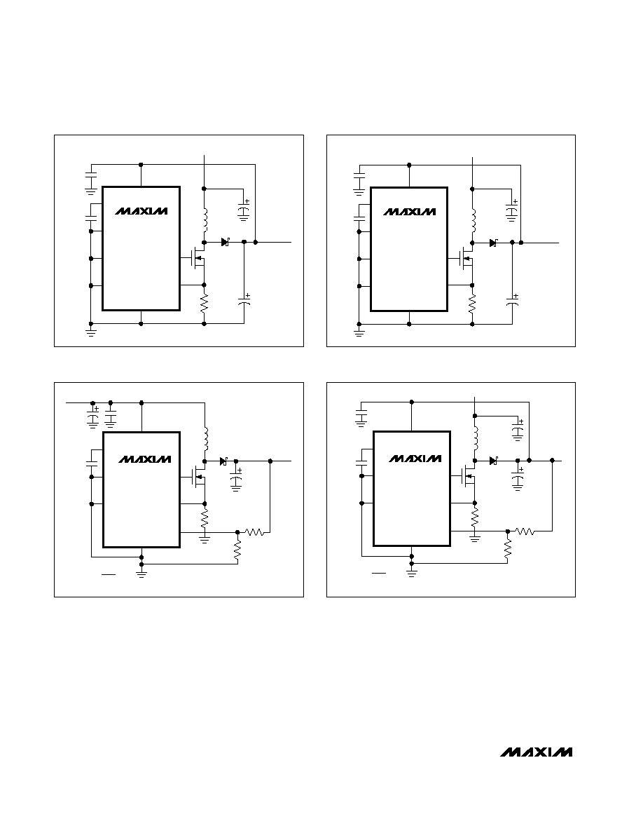
Bootstrapped/Non-Bootstrapped Modes
Figures 2 and 3 show standard application circuits for
bootstrapped and non-bootstrapped modes. In boot-
strapped mode, the IC is powered from the output
(V
OUT
, which is connected to V+) and the input voltage
range is 2V to V
OUT
. The voltage applied to the gate of
the external power transistor is switched from V
OUT
to
ground, providing more switch gate drive and thus
reducing the transistor's on resistance.
In non-bootstrapped mode, the IC is powered from the
input voltage (V+) and operates with minimum supply
current. In this mode, FB is the output voltage sense
point. Since the voltage swing applied to the gate of the
external power transistor is reduced (the gate swings
from V+ to ground), the power transistor's on resistance
increases at low input voltages. However, the supply
current is also reduced because V+ is at a lower volt-
age, and because less energy is consumed while
charging and discharging the external MOSFET's gate
capacitance. The minimum input voltage for the
MAX770MAX773 is 3V when using external feedback
resistors. With supply voltages below 5V, bootstrapped
mode is recommended.
Note: When using the MAX770/MAX771/MAX772 in
non-bootstrapped mode, there is no preset output
operation because V+ is also the output voltage
sense point for fixed-output operation. External
resistors must be used to set the output voltage.
Use 1% external feedback resistors when operating
in adjustable-output mode (Figures 2c, 2d, 3b, 3d, 3e)
to achieve an overall output voltage accuracy of ±5%.
The MAX773 can be operated in non-bootstrapped
mode without using external feedback resistors
because V+ does not act as the output voltage sense
point with preset-output operation. To achieve high-
est efficiency, operate in bootstrapped mode when-
ever possible.
MAX773 Shunt-Regulator Operation
The MAX773 has an internal 6V shunt regulator that
allows the device to step up from very high input
voltages (Figure 4).
PIN
NAME
FUNCTION
MAX770
MAX771
MAX772
MAX773
--
13
EXTH
--
12
EXTL
Low-level gate/base drive for external power transistor. Connect to the gate of an external
N-channel MOSFET or to the base of an external NPN transistor.
--
14
V15
Input sense point for 15V-output operation. Connect V
OUT
to V15 for 15V-output operation.
Leave unconnected for adjustable-output operation
_________________________________________________Pin Description (continued)
High-level gate/base drive for external power transistor. Connect to EXTL when using an external
N-channel MOSFET. When using an external NPN transistor, connect a resistor R
BASE
from
EXTH to the base of the NPN to set the maximum base-drive current.

Floating the shunt-regulator ground (SGND) disables
the shunt regulator. To enable it, connect SGND to
GND. The shunt regulator requires 1mA minimum cur-
rent for proper operation; the maximum current must
not exceed 20mA. The MAX773 operates in non-boot-
strapped mode when the shunt regulator is used, and
EXT swings between the 6V shunt-regulator voltage
and GND.
When using the shunt regulator, use an N-channel pow-
er FET instead of an NPN power transistor as the power
switch. Otherwise, excessive base drive will collapse
the shunt regulator.
External Power-Transistor
Control Circuitry
PFM Control Scheme
The MAX770MAX773 use a proprietary current-limited
PFM control scheme to provide high efficiency over a
wide range of load currents. This control scheme com-
bines the ultra-low supply current of PFM converters (or
pulse skippers) with the high full-load efficiency of
PWM converters.
Unlike traditional PFM converters, the MAX770
MAX773 use a sense resistor to control the peak induc-
tor current. They also operate with high switching
MAX770MAX773
5V/12V/15V or Adjustable, High-Efficiency,
Low I
Q
, Step-Up DC-DC Controllers
_______________________________________________________________________________________
9
V+
EXT
CONTROL
1.5V
REFERENCE
Q
TRIG
Q
S
F/F
R
Q
TRIG
LOW-VOLTAGE
OSCILLATOR
2.5V
0.1V
0.2V
ONE-SHOT
ONE-SHOT
CURRENT-SENSE
AMPLIFIER
DUAL-MODE
COMPARATOR
LBO V15
V12
V5
FB
LBI
REF
200mV
ERROR
COMPARATOR
SHDN
V+
SGND
6V
EXTH
EXTL
EXT
CS
MAX773 ONLY
MAX770
MAX771
MAX772
MAX770
MAX771
MAX772
BIAS
CIRCUITRY
N
N
N
MAX770MAX773
MAX773
ONLY
Figure 1. Block Diagram
MAX770MAX773
frequencies (up to 300kHz), allowing the use of tiny
external components.
As with traditional PFM converters, the power transistor
is not turned on until the voltage comparator senses
that the output is out of regulation. However, unlike tra-
ditional PFM converters, the MAX770MAX773 switch
using the combination of a peak current limit and a pair
of one-shots that set the maximum on-time (16µs) and
minimum off-time (2.3µs); there is no oscillator. Once
off, the minimum off-time one-shot holds the switch
off for 2.3µs. After this minimum time, the switch either
1) stays off if the output is in regulation, or 2) turns on
again if the output is out of regulation.
The control circuitry allows the ICs to operate in contin-
uous-conduction mode (CCM) while maintaining high
efficiency with heavy loads. When the power switch is
5V/12V/15V or Adjustable, High-Efficiency,
Low I
Q
, Step-Up DC-DC Controllers
10
______________________________________________________________________________________
MAX770
V
IN
= 3V
REF
SHDN
FB
AGND
GND
N
7
EXT
CS
C2
0.1
µ
F
C1
100
µ
F
L1
22
µ
H
D1
1N5817
MTP3055EL
R
SENSE
75m
C4
300
µ
F
C3
0.1
µ
F
5
4
3
6
1
8
2
V+
V
OUT
= 5V
@ 1A
Figure 2a. 5V Preset Output, Bootstrapped
Figure 2b. 12V Preset Output, Bootstrapped
Figure 2c. 12V Output, Non-Bootstrapped
Figure 2d. 9V Output, Bootstrapped
MAX770
MAX771
MAX772
V
IN
= 5V
REF
SHDN
AGND
GND
N
7
EXT
CS
FB
L1
22
µ
H
D1
1N5817
R1
18k
C4
200
µ
F
C3
0.1
µ
F
5
4
6
1
8
3
2
V+
C1
68
µ
F
V
OUT
= 12V
@ 0.5A
R2
127k
R
SENSE
100m
C2
0.1
µ
F
V
OUT
V
REF
R2 = (R1)
(
-1
)
V
REF
= 1.5V
MAX770
MAX771
MAX772
REF
SHDN
AGND
GND
N
7
EXT
CS
FB
C1
47
µ
F
L1
20
µ
H
D1
1N5817
R1
28k
C4
100
µ
F
C3
0.1
µ
F
5
4
6
1
8
3
2
V+
V
OUT
= 9V
R2
140k
R
SENSE
C2
0.1
µ
F
V
OUT
V
REF
R2 = (R1)
(
-1
)
V
REF
= 1.5V
Si9410DY
V
IN
= 4V
MAX771
V
IN
= 5V
REF
SHDN
FB
AGND
GND
N
7
EXT
CS
C2
0.1
µ
F
C1
68
µ
F
L1
22
µ
H
D1
1N5817
Si9410DY
R
SENSE
100m
C4
200
µ
F
C3
0.1
µ
F
5
4
3
6
1
8
2
V+
V
OUT
= 12V
@ 0.5A

MAX770MAX773
5V/12V/15V or Adjustable, High-Efficiency,
Low I
Q
, Step-Up DC-DC Controllers
______________________________________________________________________________________
11
GND
MAX773
C3
0.1
µ
F
V
OUT
= 12V
V+
R4
63.4k
(1%)
R3
10k
(1%)
SGND
LBO
EXTH
8
5
7
6
EXTL
CS
V12
V15
V5
REF
LBI
SHDN
FB
2
14
1
10
4
13
12
11
9
R
SENSE
N
Si9410DY
C4
C2
0.1
µ
F
VIN
L1
22
µ
H
D1
1N5817
100k
C1
R4 = R3
(
V
TRIP
-1
)
V
REF
MIN NOMINAL MAX
10.6 11.0 11.4
V
TRIP
(V)
3
V
REF
= 1.5V
GND
MAX773
C3
0.1
µ
F
V+
EXTL
CS
V12
8
5
7
V5
FB
SGND
LBO
REF
LBI
SHDN
4
10
12
11
1
2
6
9
R
SENSE
0.4
C4
150
µ
F
C2
0.1
µ
F
D1
1N5818
V15
14
EXTH
13
C1
47
µ
F
3
L1
150
µ
H
910
R1
34k
R2
510k
ZTX694B
V
OUT
= 24V
@ 30mA
V
IN
= 5V
V
OUT
V
REF
R2 = (R1)
(
-1
)
V
REF
= 1.5V
GND
MAX773
C3
0.1
µ
F
V+
EXTL
CS
V5
8
7
6
V15
V12
SGND
LBO
REF
SHDN
FB
4
10
V
IN
= 5V
12
11
2
14
1
9
R
SENSE
C4
C2
0.1
µ
F
D1
1N5817
EXTH
13
3
L1
22
µ
H
V
OUT
= 15V
LBI
N
Si9410DY
5
C1
GND
MAX773
C3
0.1
µ
F
V+
EXTL
CS
V5
8
5
7
V15
V12
LBO
REF
LBI
SHDN
4
VIN
12
11
2
14
1
9
R
SENSE
C4
D1
1N5817
EXTH
13
3
L1
20
µ
H
V
OUT
= 16V
SGND
N
10
C1
C2
0.1
µ
F
FB 6
R2
133k
R1
13.7k
V
OUT
V
REF
R2 = (R1)
(
-1
)
V
REF
= 1.5V
Si9410DY
Figure 3a. 12V Preset Output, Bootstrapped, N-Channel
Power MOSFET
Figure 3b. 24V Output, Non-Bootstrapped, NPN Power
Transistor
Figure 3c. 15V Preset Output, Non-Bootstrapped N-Channel
Power MOSFET
Figure 3d. 16V Output, Bootstrapped, N-Channel
Power MOSFET

MAX770MAX773
turned on, it stays on until either 1) the maximum on-
time one-shot turns it off (typically 16µs later), or 2) the
switch current reaches the peak current limit set by the
current-sense resistor.
To increase light-load efficiency, the current limit for the
first two pulses is set to one-half the peak current limit.
If those pulses bring the output voltage into regulation,
the error comparator holds the MOSFET off and the
current limit remains at one-half the peak current limit. If
the output voltage is still out of regulation after two
pulses, the current limit for the next pulse is raised to
the peak current limit set by the external sense resistor
(see inductor current waveforms in the
Typical
Operating Characteristics).
The MAX770MAX773 switching frequency is variable
(depending on load current and input voltage), causing
variable switching noise. However, the subharmonic
noise generated does not exceed the peak current limit
times the filter capacitor equivalent series resistance
(ESR). For example, when generating a 12V output at
500mA from a 5V input, only 180mV of output ripple
occurs using the circuit of Figure 2b.
Low-Voltage Start-Up Oscillator
The MAX770/MAX771/MAX772 feature a low input volt-
age start-up oscillator that guarantees start-up with no
load down to 2V when operating in bootstrapped mode
and using internal feedback resistors. At these low volt-
ages, the supply voltage is not large enough for proper
error-comparator operation and internal biasing. The
start-up oscillator has a fixed 50% duty cycle and the
MAX770/MAX771/MAX772 disregard the error-com-
parator output when the supply voltage is less than
2.5V. Above 2.5V, the error-comparator and normal one-
shot timing circuitry are used. The low voltage start-up
circuitry is disabled if non-bootstrapped mode is select-
ed (FB is not tied to ground).
The MAX773 does not provide the low-voltage 50%
duty-cycle oscillator. Its minimum start-up voltage is 3V
for all modes.
External Transistor
An N-FET power switch is recommended for the
MAX770/MAX771/MAX772.
The MAX773 can drive either an N-channel MOSFET
(N-FET) or an NPN because it provides two separate
5V/12V/15V or Adjustable, High-Efficiency,
Low I
Q
, Step-Up DC-DC Controllers
12
______________________________________________________________________________________
GND
MAX773
C3
0.1
µ
F
v+
EXTL
CS
V5
8
5
7
V15
V12
LBO
REF
LBI
SHDN
4
12
11
2
14
1
9
R
SENSE
1.0
C4
100
µ
F
D1
MUR115
EXTH
13
3
L1
250
µ
H
V
OUT
= 100V
@ 10mA
SGND
N
10
C1
47
µ
F
FB
6
R2
732k (1%)
R1
11.3k (1%)
Si9420DY
R
SHUNT
3k
C2
0.1
µ
F
V
IN
= 24V TO 28V
V
OUT
V
REF
R2 = (R1)
(
-1
)
V
REF
= 1.5V
MAX773
R
SHUNT
C2
0.1
µ
F
SGND
6V (typ)
V+
V
IN
R
SHUNT =
V
IN (MIN)
- V
SHUNT
(
MAX
)
I
SHUNT
*
*
SEE TEXT FOR I
SHUNT
CALCULATION
3
10
Figure 3e. 100V Output, Shunt Regulator, N-Channel Power
MOSFET
Figure 4. MAX773 Shunt Regulator
drive outputs (EXTH and EXTL) that operate 180° out of
phase (Figures 3a and 3b). In Figure 3b, the resistor in
series with EXTH limits the base current, and EXTL (which
is connected directly to the base) turns the transistor off.
Shutdown Mode
When SHDN is high, the MAX770MAX773 enter shut-
down mode. In this mode, the internal biasing circuit-
ry is turned off (including the reference) and V
OUT
falls to a diode drop below V
IN
(due to the DC path
from the input to the output). In shutdown mode, the
supply current drops to less than 5µA. SHDN is a
TTL/CMOS logic-level input. Connect SHDN to GND for
normal operation.
The MAX773's shunt regulator is
not
disabled in shut-
down mode.
Low-Battery Detector
The MAX773 provides a low-battery comparator that
compares the voltage on LBI to the reference voltage.
When the LBI voltage is below V
REF,
LBO (an open-
drain output) goes low. The low-battery comparator's
20mV of hysteresis adds noise immunity, preventing
repeated triggering of LBO. Use a resistor-divider network
between V+, LBI, and GND to set the desired trip voltage
V
TRIP
. LBO is high impedance in shutdown mode.
__________________Design Procedure
Setting the Output Voltage
To set the output voltage, first determine the mode of
operation, either bootstrapped or non-bootstrapped.
Bootstrapped mode provides more output current
capability, while non-bootstrapped mode reduces the
supply current (see
Typical Operating Characteristics).
If a decaying voltage source (such as a battery) is
used, see the additional notes in the
Low Input Voltage
Operation section.
Use the MAX770/MAX771/MAX772 unless one or more
of the following conditions applies. If one or more of the
following is true, use the MAX773:
1) An NPN power transistor will be used as the power
switch
2) The LBI/LBO function is required
3) The shunt regulator must accommodate a high
input voltage
4) Preset-output non-bootstrapped operation is
desired--for example, to reduce the no-load
supply current in a 5V to 12V application.
See Table 1 for a summary of operating characteristics
and requirements for the ICs in bootstrapped and non-
bootstrapped modes.
The MAX770MAX773's output voltage can be adjust-
ed from very high voltages down to 3V, using external
resistors R1 and R2 configured as shown in Figure 5.
For adjustable-output operation, select feedback resis-
tor R1 in the range of 10k
to 500k
. R2 is given by:
V
OUT
R2 = (R1)
(
-1
)
V
REF
where V
REF
equals 1.5V.
For preset-output operation, tie FB to GND (this
forces bootstrapped-mode operation for the
MAX770/MAX771/MAX772).
Configure the MAX773 for a preset voltage of 5V, 12V, or
15V by connecting the output to the corresponding
sense input pin (i.e., V5, V12, or V15). FB must be tied to
ground for preset-output operation. Leave all unused
sense input pins unconnected. Failure to do so will cause
an incorrect output voltage. The MAX773 can provide
a preset output voltage in both bootstrapped and non-
bootstrapped modes.
Figures 2 and 3 show various circuit configurations for
bootstrapped/non-bootstrapped, preset/adjustable
operation.
Shunt-Regulator Operation
When using the shunt regulator, connect SGND to ground
and place a 0.1µF capacitor between V+ and SGND, as
close to the IC as possible. Increase C2 to 1.0µF to
improve shunt regulators performance with heavy loads.
Select R
SHUNT
such that 1mA
I
SHUNT
20mA.
MAX770MAX773
5V/12V/15V or Adjustable, High-Efficiency,
Low I
Q
, Step-Up DC-DC Controllers
______________________________________________________________________________________
13
MAX770
MAX771
MAX772
MAX773
R1
R2
GND
FB
V
OUT
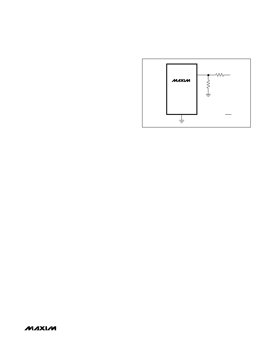
R1 = 10k TO 500k
V
OUT
V
REF
R2 = R1
(
-1
)
V
REF
= 1.5V
Figure 5. Adjustable Output Circuit
MAX770MAX773
Use an N-channel FET as the power switch when using
the shunt regulator (see
MAX773 Shunt-Regulator
Operation in the Detailed Description). The shunt-regu-
lator current powers the MAX773 and also provides the
FET gate-drive current, which depends largely on the
FET's total gate charge at V
GS
= 5V. To determine the
shunt-resistor value, first determine the maximum shunt
current required.
I
SHUNT
= I
SUPP
+ I
GATE
See
N-Channel MOSFETs in the Power-Transistor
Selection section to determine I
GATE
.
Determine the shunt-resistor value using the following
equation:
V
IN
(min) - V
SHUNT
(max)
R
SHUNT
(max) = ------------------------
I
SHUNT
where V
SHUNT
(max) is 6.3V.
The shunt regulator is not disabled in shutdown
mode, and continues to draw the calculated shunt
current.
If the calculated shunt regulator current exceeds 20mA,
or if the shunt current exceeds 5mA and less shunt reg-
ulator current is desired, use the circuit of Figure 6 to
provide increased drive and reduced shunt current
when driving N-FETs with large gate capacitances.
Select I
SHUNT
= 3mA. This provides adequate biasing
current for this circuit, although higher shunt currents
can be used.
To prevent the shunt regulator from drawing current in
shutdown mode, place a switch in series with the shunt
resistor.
5V/12V/15V or Adjustable, High-Efficiency,
Low I
Q
, Step-Up DC-DC Controllers
14
______________________________________________________________________________________
MAX773(N)/MAX773(S)
MAX770MAX773(N)
Fixed Output Available
Higher
Lower
GND to V
OUT
2V to 5V (MAX770/MAX771/MAX772),
3V to 5V (MAX773)
MAX770MAX773(N)
Higher
2V to 16.5V (MAX770/MAX771/MAX772),
(internal feedback resistors)
3V to 16.5V (MAX770/MAX771/MAX772),
(external feedback resistors)
3V to 16.5V (MAX773)
BOOTSTRAPPED*
MAX770/MAX771/MAX772/
MAX773(N)/MAX773(S)
Adjustable Output Available
Lower
Gate-Drive Capacitive Losses
Higher
FET On Resistance
GND to V+
Gate Drive
5V to 16.5V
(MAX770/MAX771/MAX772),
5V and up (MAX773)
Normally Recommended Input
Voltage Range
Lower
No-Load Supply Current
3V to 16.5V
(MAX770/MAX771/MAX772),
3V and up (MAX773)
Possible Input Voltage Range
NON-BOOTSTRAPPED
PARAMETER
Table 1. Bootstrapped vs. Non-Bootstrapped Operation
MAX773
CS
FB
SGND
R
SHUNT
N
EXTL
100
V+
C1
C2
0.1
µ
F
V
IN
L1
20
µ
H
NPN
2N2222A
R2
R1
D1
V
OUT
C4
R
SENSE
PNP
2N2907A
3
10
13
12
11
6
EXTH
Figure 6. Increased N-FET Gate Drive when Using the Shunt
Regulator
*MAX773(S) indicates shunt mode; MAX773(N) indicates NOT in shunt mode.
Determining R
SENSE
The
Typical Operating Characteristics graphs show the
output current capability for various modes, sense
resistors, and input/output voltages. Use these graphs,
along with the theoretical output current curves shown
in Figures 7a-7d, to select R
SENSE
. These theoretical
curves assume that an external N-FET power switch is
used. They were derived using the minimum (worst-
case) current-limit comparator threshold value, and the
inductance value. No tolerance was included for
R
SENSE
. The voltage drop across the diode was
assumed to be 0.5V, and the drop across the power
switch r
DS(ON)
and coil resistance was assumed to be
0.3V. To use the graphs, locate the graph with the
appropriate output voltage or the graph having the
nearest output voltage higher than the desired output
voltage. On this graph, find the curve for the largest
sense-resistor value with an output current that is ade-
quate at the lowest input voltage.
Determining the Inductor (L)
Practical inductor values range from 10µH to 300µH.
20µH is a good choice for most applications. In appli-
cations with large input/output differentials, the IC's
output current capability will be much less when the
inductance value is too low, because the IC will always
operate in discontinuous mode. If the inductor value
is too low, the current will ramp up to a high level
before the current-limit comparator can turn off the
switch. The minimum on-time for the switch (t
ON
(min))
is approximately 2µs; select an inductor that allows
the current to ramp up to I
LIM
/2 in no less than 2µs.
Choosing a value of I
LIM
/2 allows the half-size current
pulses to occur, increasing light-load efficiency and
minimizing output ripple.
MAX770MAX773
5V/12V/15V or Adjustable, High-Efficiency,
Low I
Q
, Step-Up DC-DC Controllers
______________________________________________________________________________________
15
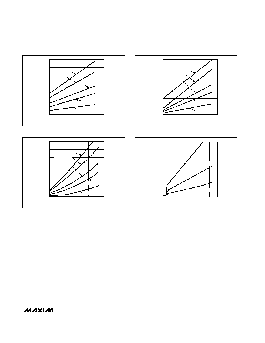
MAXIMUM OUTPUT CURRENT (A)
0
INPUT VOLTAGE (V)
0.5
1.0
1.5
2.0
2.5
3.0
3.5
2
3
4
5
R
SENSE
= 40m
R
SENSE
= 50m
R
SENSE
= 75m
R
SENSE
= 200m
R
SENSE
= 100m
V
OUT
= 5V
L = 22
µ
H
MAXIMUM OUTPUT CURRENT (A)
0
INPUT VOLTAGE (V)
0.5
1.0
1.5
2.0
2.5
3.0
3.5
2
4
6
8
10
12
R
SENSE
= 200m
R
SENSE
= 100m
R
SENSE
= 40m
R
SENSE
= 50m
R
SENSE
= 75m
V
OUT
= 12V
L = 22
µ
H
Figure 7a. Maximum Output Current vs. Input Voltage
(V
OUT
= 5V)
Figure 7b. Maximum Output Current vs. Input Voltage
(V
OUT
= 12V)
Figure 7c. Maximum Output Current vs. Input Voltage
(V
OUT
= 15V)
Figure 7d. Maximum Output Current vs. Input Voltage
(V
OUT
= 24V)
MAXIMUM OUTPUT CURRENT (A)
0
INPUT VOLTAGE (V)
0.5
1.0
1.5
2.0
2.5
3.0
3.5
2
4
6
8
10
12
14
16
R
SENSE
= 200m
R
SENSE
= 100m
V
OUT
= 15V
L = 22
µ
H
R
SENSE
= 40m
R
SENSE
= 50m
R
SENSE
= 75m
MAXIMUM OUTPUT CURRENT (A)
0
2
INPUT VOLTAGE (V)
0.8
6
10
14
0.2
0.4
0.6
V
OUT
= 24V
L =150
µ
H
R
SENSE
= 100m
R
SENSE
= 200m
R
SENSE
= 400m
MAX770MAX773
The standard operating circuits use a 22µH inductor.
If a different inductance value is desired, select L
such that:
V
IN
(max) x t
ON
(min)
L
--------------------
I
LIM
/ 2
Larger inductance values tend to increase the start-up
time slightly, while smaller inductance values allow the
coil current to ramp up to higher levels before the
switch turns off, increasing the ripple at light loads.
Inductors with a ferrite core or equivalent are recom-
mended; powder iron cores are not recommended for
use with high switching frequencies. Make sure the
inductor's saturation current rating (the current at which
the core begins to saturate and the inductance starts to
fall) exceeds the peak current rating set by R
SENSE
.
However, it is generally acceptable to bias the inductor
into saturation by approximately 20% (the point where
the inductance is 20% below the nominal value). For
highest efficiency, use a coil with low DC resistance,
preferably under 20m
. To minimize radiated noise,
use a toroid, a pot core, or a shielded coil.
Table 2 lists inductor suppliers and specific recom-
mended inductors.
Power Transistor Selection
Use an N-channel MOSFET power transistor with the
MAX770/MAX771/MAX772 (Figure 8a).
Use an N-FET whenever possible with the MAX773. An
NPN transistor can be used, but be extremely careful
when determining the base current (see
NPN
Transistors section). An NPN transistor is not recom-
mended when using the shunt regulator.
N-Channel MOSFETs
To ensure the external N-channel MOSFET (N-FET) is
turned on hard, use logic-level or low-threshold
N-FETs when the input drive voltage is less than 8V. This
applies even in bootstrapped mode, to ensure start-up.
N-FETs provide the highest efficiency because they do
not draw any DC gate-drive current, but they are typi-
cally more expensive than NPN transistors. When using
an N-FET with the MAX773, connect EXTH and EXTL to
the N-FET's gate (Figure 8b).
When selecting an N-FET, three important parameters
are the total gate charge (Q
g
), on resistance (r
DS(ON)
),
and reverse transfer capacitance (C
RSS
).
Q
g
takes into account all capacitances associated with
charging the gate. Use the typical Q
g
value for best
results; the maximum value is usually grossly over-
specified since it is a guaranteed limit and not the mea-
sured value. The typical total gate charge should be
50nC or less. With larger numbers, the EXT pins may
not be able to adequately drive the gate. The EXT
rise/fall time with various capacitive loads as shown in
the
Typical Operating Characteristics.
5V/12V/15V or Adjustable, High-Efficiency,
Low I
Q
, Step-Up DC-DC Controllers
16
______________________________________________________________________________________
MAX770
MAX771
MAX772
N
EXT
CS
R
SENSE
MAX773
NPN
EXTH
EXTL
CS
L
R
SENSE
R
BASE
I
C(PEAK)
I
B
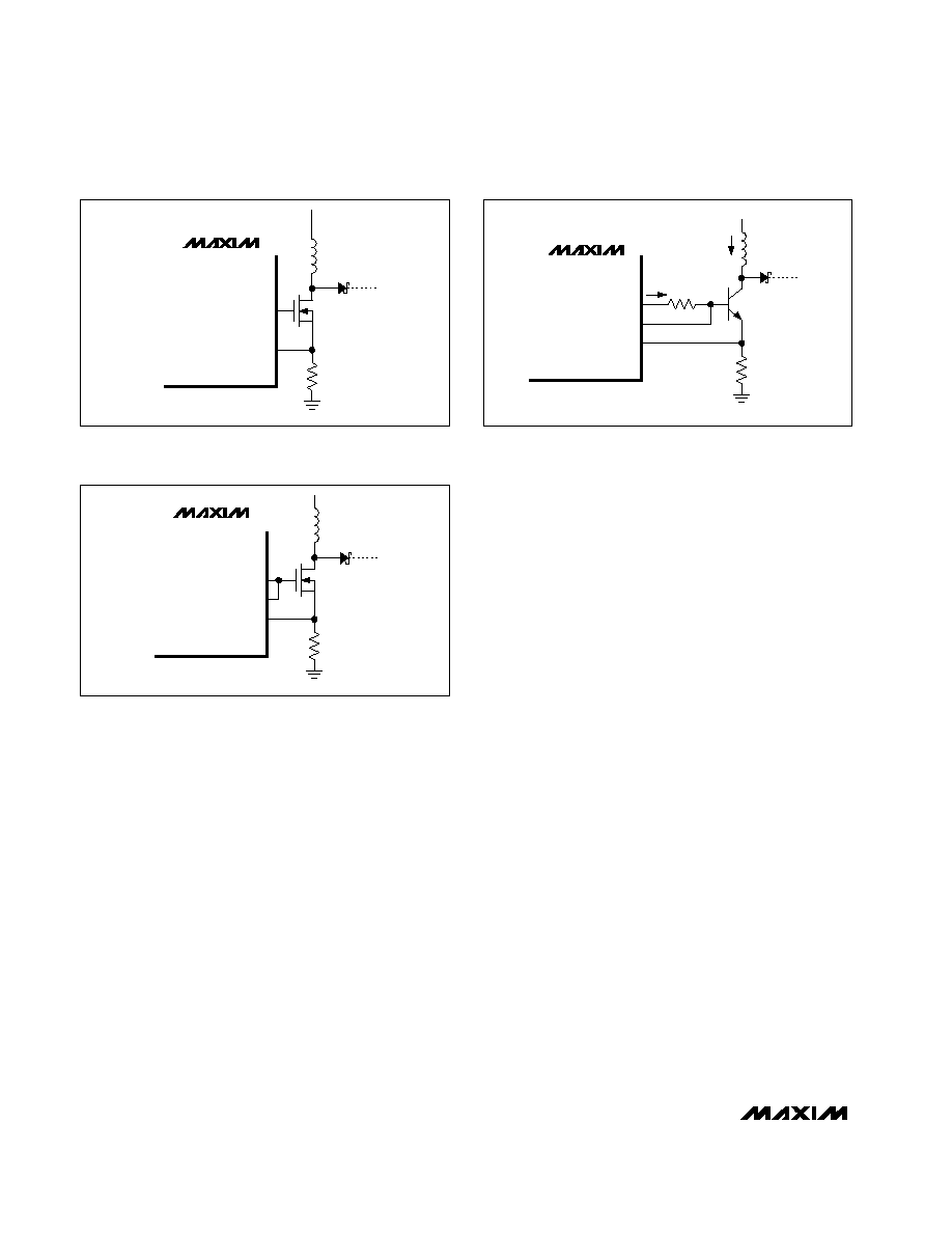
Figure 8a. Use an N-Channel MOSFET with the
MAX770/MAX771/MAX772
Figure 8b. Using an N-Channel MOSFET with the MAX773
Figure 8c. Using an NPN Transistor with the MAX773
MAX773
N
EXTH
EXTL
CS
L
R
SENSE

The two most significant losses contributing to the
N-FET's power dissipation are I
2
R losses and switching
losses. Select a transistor with low r
DS(ON)
and low
C
RSS
to minimize these losses.
Determine the maximum required gate-drive current
from the Q
g
specification in the N-FET data sheet.
The MAX773's maximum allowed switching frequency
during normal operation is 300kHz; but at start-up the
maximum frequency can be 500kHz, so the maximum
current required to charge the N-FET's gate is
f(max) x Q
g
(typ). Use the typical Q
g
number from the
transistor data sheet. For example, the Si9410DY has a
Q
g
(typ) of 17nC (at V
GS
= 5V), therefore the current
required to charge the gate is:
I
GATE
(max) = (500kHz) (17nC) = 8.5mA.
The bypass capacitor on V+ (C2) must instantaneously
furnish the gate charge without excessive droop (e.g.,
less than 200mV):
Q
g
V+ = ----
C2
Continuing with the example,
V+ = 17nC/0.1µF = 170mV.
Use I
GATE
when calculating the appropriate shunt
resistor. See the
Shunt Regulator Operation section.
Figure 2a's application circuit uses an MTD3055EL
logic-level N-FET with a guaranteed threshold voltage
(V
TH
) of 2V. Figure 2b's application circuit uses an
8-pin Si9410DY surface-mount N-FET that has 50m
on resistance with 4.5V V
GS
, and a guaranteed V
TH
of
less than 3V.
NPN Transistors
The MAX773 can drive NPN transistors, but be
extremely careful when determining the base-current
requirements. Too little base current can cause exces-
sive power dissipation in the transistor; too much base
current can cause the base to oversaturate, so the tran-
sistor remains on continually. Both conditions can dam-
age the transistor.
When using the MAX773 with an NPN transistor, con-
nect EXTL to the transistor's base, and connect R
BASE
between EXTH and the base (Figure 8c).
To determine the required peak inductor current,
I
C(PEAK
), observe the
Typical Operating Characteristics
efficiency graphs and the theoretical output current
capability vs. input voltage graphs to determine a
sense resistor that will allow the desired output current.
Divide the 170mV worst-case (smallest) voltage across
the current-sense amplifier V
CS
(max) by the sense-
resistor value. To determine I
B
, set the peak inductor
current (I
LIM)
equal to the peak transistor collector cur-
rent I
C(PEAK)
. Calculate I
B
as follows:
I
B
= I
LIM
/ß
Use the worst-case (lowest) value for ß given in the
transistor's electrical specification, where the collector
current used for the test is approximately equal to I
LIM
.
It may be necessary to use even higher base currents
(e.g., I
B
= I
LIM
/10), although excessive I
B
may impair
operation by extending the transistor's turn-off time.
R
BASE
is determined by:
(
V
EXTH
- V
BE
- V
CS
(min )
)
R
BASE
= ------------------------
I
B
Where V
EXTH
is the voltage at V+ (in bootstrapped
mode V
EXTH
is the output voltage), V
BE
is the 0.7V
transistor base-emitter voltage, V
CS
(min) is the voltage
drop across the current-sense resistor, and I
B
is the
minimum base current that forces the transistor into
saturation. This equation reduces to (V+ - 700mV -
170mV) / I
B
.
For maximum efficiency, make R
BASE
as large as pos-
sible, but small enough to ensure the transistor is
always driven near saturation. Highest efficiency is
obtained with a fast-switching NPN transistor
(f
T
150MHz) with a low collector-emitter saturation
voltage and a high current gain. A good transistor to
use is the Zetex ZTX694B.
Diode Selection
The MAX770MAX773's high switching frequency
demands a high-speed rectifier. Schottky diodes such
as the 1N58171N5822 are recommended. Make sure
that the Schottky diode's average current rating
exceeds the peak current limit set by R
SENSE
, and that
its breakdown voltage exceeds V
OUT
. For high-temper-
ature applications, Schottky diodes may be inadequate
due to their high leakage currents; high-speed silicon
diodes may be used instead. At heavy loads and high
temperatures, the benefits of a Schottky diode's low for-
ward voltage may outweigh the disadvantages of its
high leakage current.
Capacitor Selection
Output Filter Capacitor
The primary criterion for selecting the output filter
capacitor (C2) is low effective series resistance (ESR).
The product of the peak inductor current and the output
filter capacitor's ESR determines the amplitude of the
ripple seen on the output voltage. An OS-CON 300µF,
6.3V output filter capacitor has approximately 50m
of
ESR and typically provides 180mV ripple when
stepping up from 3V to 5V at 1A (Figure 2a).
MAX770MAX773
5V/12V/15V or Adjustable, High-Efficiency,
Low I
Q
, Step-Up DC-DC Controllers
______________________________________________________________________________________
17
MAX770MAX773
Smaller capacitors are acceptable for light loads or in
applications that can tolerate higher output ripple.
Since the output filter capacitor's ESR affects efficien-
cy, use low-ESR capacitors for best performance. The
smallest low-ESR surface-mount tantalum capacitors
currently available are the Sprague 595D series. Sanyo
OS-CON organic semiconductor through-hole capaci-
tors and the Nichicon PL series also exhibit low ESR.
See Table 2.
Input Bypass Capacitors
The input bypass capacitor (C1) reduces peak currents
drawn from the voltage source and also reduces noise
at the voltage source caused by the switching action of
the MAX770MAX773. The input voltage source imped-
ance determines the size of the capacitor required at
the V+ input. As with the output filter capacitor, a low-
ESR capacitor is recommended. For output currents up
to 1A, 150µF (C1) is adequate, although smaller
bypass capacitors may also be acceptable.
Bypass the IC with a 0.1µF ceramic capacitor (C2)
placed close to the V+ and GND pins.
Reference Capacitor
Bypass REF with a 0.1µF capacitor (C3). REF can
source up to 100µA of current.
Setting the Low-Battery-Detector Voltage
To set the low-battery detector's falling trip voltage
(V
TRIP
(falling)), select R3 between 10k
and 500k
(Figure 9), and calculate R4 as follows:
V
TRIP
- V
REF
R4 = (R3)
(
--------------
)
V
REF
where V
REF
= 1.5V.
The rising trip voltage is higher because of the com-
parator's approximately 20mV of hysteresis, and is
determined by:
R4
V
TRIP
(rising) = (V
REF
+ 20mV) (1 + ----)
R3
Connect a high value resistor (larger than R3 + R4)
between LBI and LBO if additional hysteresis is required.
Connect a pull-up resistor (e.g., 100k
) between LBO
and V+. Tie LBI to GND and leave LBO floating if the
low-battery detector is not used.
__________Applications Information
MAX773 Operation with High
Input/Output Voltages
The MAX773's shunt regulator input allows high volt-
ages to be converted to very high voltages. Since the
MAX773 runs off the 6V shunt (bootstrapped operation
is not allowed), the IC will not see the high input volt-
age. Use an external logic-level N-FET as the power
switch, since only 6V of V
GS
are available. Also, make
sure all external components are rated for very high
output voltage. Figure 3e shows a circuit that converts
28V to 100V.
Low Input Voltage Operation
When using a power supply that decays with time
(such as a battery), the N-FET transistor will operate in
its linear region when the voltage at EXT approaches
the threshold voltage of the FET, dissipating excessive
power. Prolonged operation in this mode may damage
the FET. This effect is much more significant in non-
bootstrapped mode than in bootstrapped mode, since
bootstrapped mode typically provides much higher
V
GS
voltages. To avoid this condition, make sure V
EXT
is above the V
TH
of the FET, or use a voltage detector
(such as the MAX8211) to put the IC in shutdown mode
once the input supply voltage falls below a predeter-
mined minimum value. Excessive loads with low input
voltages can also cause this condition.
5V/12V/15V or Adjustable, High-Efficiency,
Low I
Q
, Step-Up DC-DC Controllers
18
______________________________________________________________________________________
MAX773
LBI
LBO
GND
V+
R4
V
IN
R5
100k
R3
LOW-BATTERY
OUTPUT
V
TRIP
V
REF
R4 = R3
(
-1
)
V
REF
= 1.5V
Figure 9. Input Voltage Monitor Circuit
Starting Up under Load
The
Typical Operating Characteristics show the Start-
Up Voltage vs. Load Current graph for bootstrapped-
mode operation. This graph depends on the type
of power switch used. The MAX770MAX773 are
not designed to start up under full load in boot-
strapped mode with low input voltages.
Layout Considerations
Due to high current levels and fast switching wave-
forms, which radiate noise, proper PC board layout is
essential. Protect sensitive analog grounds by using a
star ground configuration. Minimize ground noise by
connecting GND, the input bypass capacitor ground
lead, and the output filter capacitor ground lead to a
single point (star ground configuration). Also, minimize
lead lengths to reduce stray capacitance, trace resis-
tance, and radiated noise. Place input bypass capaci-
tor C2 as close as possible to V+ and GND.
Excessive noise at the V+ input may falsely trigger the
timing circuitry, resulting in short pulses at EXT. If this
occurs it will have a negligible effect on circuit efficien-
cy. If desired, place a 4.7µF directly across the V+ and
GND pins (in parallel with the 0.1µF C2 bypass capaci-
tor) to reduce the noise at V+.
MAX770MAX773
5V/12V/15V or Adjustable, High-Efficiency,
Low I
Q
, Step-Up DC-DC Controllers
______________________________________________________________________________________
19
Table 2. Component Suppliers
PRODUCTION
INDUCTORS
CAPACITORS
TRANSISTORS
Surface Mount
Matsuo
267 series
Sprague
595D series
Through Hole
Sumida
CD54 series
CDR125 series
Coiltronics
CTX20 series
Motorola
1N58171N5822
MUR115 (high voltage)
Nihon
EC10 series
DIODES
Sumida
RCH855 series
RCH110 series
Renco
RL1284-18
Sanyo
OS-CON series
Nichicon
PL series
United Chemi-Con
LXF series
NPN
Zetex
ZTX694B
Coiltronics
Matsuo
USA: (714) 969-2491
(714) 960-6492
Japan: 81-6-337-6450
81-6-337-6456
Nichicon
USA: (847) 843-7500
(847) 843-2798
Nihon
USA: (805) 867-2555
(805) 867-2698
Renco
USA: (516) 586-5566
(516) 586-5562
Sanyo
USA: (619) 661-6835
(619) 661-1055
Japan: 81-7-2070-6306
81-7-2070-1174
Sumida
USA: (847) 956-0666
Japan: 81-3-3607-5111
81-3-3607-5144
United Chemi-Con
USA: (714) 255-9500
(714) 255-9400
N-FET
Siliconix
Si9410DY
Si9420DY (high voltage)
Motorola
MTP3055EL
MTD20N03HDL
USA: (561) 241-7876
(561) 241-9339
SUPPLIER
PHONE
FAX
Zetex
USA: (516) 543-7100
(516) 864-7630
UK: 44-61-627-4963
44-61-627-5467
MAX770MAX773
5V/12V/15V or Adjustable, High-Efficiency,
Low I
Q
, Step-Up DC-DC Controllers
20
______________________________________________________________________________________
14
13
12
11
10
9
8
1
2
3
4
5
6
7
V15
EXTH
EXTL
CS
LBO
V+
V5
V12
MAX773
SGND
GND
REF
SHDN
FB
LBI
DIP/SO
___Ordering Information (continued)
____Pin Configurations (continued)
TOP VIEW
_________________Chip Topographies
TRANSISTOR COUNT: 501;
SUBSTRATE CONNECTED TO V+.
TRANSISTOR COUNT: 501;
SUBSTRATE CONNECTED TO V+.
EXTH
EXTL
CS
SGND
GND
GND
V5
V12
V15
V+
LBO
LBI
FB
SHDN
REF
0.126"
(3.200mm)
0.080"
(2.032mm)
MAX770/MAX771/MAX772
MAX773
V+
FB
0.126"
(3.200mm)
0.080"
(2.032mm)
EXT
CS
GND
AGND
SHDN
REF
14 CERDIP
-55°C to +125°C
MAX773MJD
14 Narrow SO
-40°C to +85°C
MAX773ESD
14 Plastic DIP
-40°C to +85°C
MAX773EPD
Dice*
0°C to +70°C
MAX773C/D
14 SO
0°C to +70°C
MAX773CSD
14 Plastic DIP
0°C to +70°C
MAX773
CPD
8 CERDIP
-55°C to +125°C
MAX772MJA
8 SO
-40°C to +85°C
MAX772ESA
8 Plastic DIP
-40°C to +85°C
MAX772EPA
Dice*
0°C to +70°C
MAX772C/D
8 SO
0°C to +70°C
MAX772CSA
8 Plastic DIP
0°C to +70°C
MAX772
CPA
8 CERDIP
-55°C to +125°C
MAX771MJA
8 SO
-40°C to +85°C
MAX771ESA
8 Plastic DIP
-40°C to +85°C
MAX771EPA
Dice*
0°C to +70°C
MAX771C/D
8 SO
0°C to +70°C
MAX771CSA
8 Plastic DIP
0°C to +70°C
MAX771
CPA
PIN-PACKAGE
TEMP. RANGE
PART
*Contact factory for dice specifications.