General Description
The MAX7320 2-wire serial-interfaced peripheral fea-
tures eight push-pull outputs with selectable power-up
logic states.
The +5.5V tolerant RST input clears the serial interface,
terminating any I
2
C
communication to or from the
MAX7320.
The MAX7320 uses two address inputs with four-level
logic to allow 16 I
2
C slave addresses. The slave
address also determines the power-up state level for
the outputs in groups of four ports.
The MAX7320 supports hot insertion. The serial inter-
face SDA, SCL, AD0, AD2, and RST remain high
impedance in power-down (V+ = 0V) with up to +6V
asserted on them.
The MAX7320 is one device in a family of pin-compatible
port expanders with a choice of input ports, open-drain
I/O ports, and push-pull output ports (see Table 1).
The MAX7320 is available in 16-pin QSOP and 16-pin
TQFN packages, and is specified over the automotive
temperature range (-40°C to +125°C).
Applications
Features
o 400kHz, +5.5V-Tolerant I
2
C Serial Interface
o +1.71V to +5.5V Operating Voltage
o Eight Push-Pull Output Ports with Selectable
Power-Up Logic States
o RST Clears the Serial Interface, Terminating Any
Serial Transaction to or from the MAX7320
o AD0 and AD2 Inputs Select from 16 Slave
Addresses
o Low 0.6µA (typ) Standby Current
o -40°C to +125°C Temperature Range
MAX7320
I
2
C Port Expander with Eight Push-Pull Outputs
________________________________________________________________ Maxim Integrated Products
1
19-3879; Rev 0; 10/05
For pricing, delivery, and ordering information, please contact Maxim/Dallas Direct! at
1-888-629-4642, or visit Maxim's website at www.maxim-ic.com.
Ordering Information
PART
TEMP
RANGE
PIN-
PACKAGE
TOP
MARK
PKG
CODE
MAX7320AEE+
-40°C to
+125°C
16 QSOP
--
E16-4
MAX7320ATE+
-40°C to
+125°C
16 TQFN
3mm x 3mm
x 0.8mm
ADB
T1633-4
Pin Configurations, Typical Application Circuit, and
Functional Diagram appear at end of data sheet.
+Denotes lead-free package.
Selector Guide
PART
INPUTS
INTERRUPT MASK
OPEN-DRAIN OUTPUTS
PUSH-PULL OUTPUTS
MAX7319
8
Yes
--
--
MAX7320
--
--
--
8
MAX7321
Up to 8
--
Up to 8
--
MAX7322
4
Yes
--
4
MAX7323
Up to 4
--
Up to 4
4
MAX7328*
--
--
MAX7329**
Up to 8
--
Up to 8
--
*Second source to PCF8574.
**Second source to PCF8574A.
Purchase of I
2
C components from Maxim Integrated Products, Inc., or one of its sublicensed Associated Companies, conveys a
license under the Philips I
2
C Patent Rights to use these components in an I
2
C system, provided that the system conforms to the I
2
C
Standard Specification as defined by Philips.
Cell Phones/PDAs
Satellite Radios
Notebooks
Automotive
RAID
Servers

MAX7320
I
2
C Port Expander with Eight Push-Pull Outputs
2
_______________________________________________________________________________________
ABSOLUTE MAXIMUM RATINGS
Stresses beyond those listed under "Absolute Maximum Ratings" may cause permanent damage to the device. These are stress ratings only, and functional
operation of the device at these or any other conditions beyond those indicated in the operational sections of the specifications is not implied. Exposure to
absolute maximum rating conditions for extended periods may affect device reliability.
(All voltages referenced to GND.)
Supply Voltage V+....................................................-0.3V to +6V
SCL, SDA, AD0, AD2, RST .......................................-0.3V to +6V
O007...............................................................0.3V to V+ + 0.3V
0007 Output Current .......................................................±25mA
SDA Input Current.............................................................. 10mA
Total V+ Current..................................................................50mA
Total GND Current ...........................................................100mA
Continuous Power Dissipation (T
A
= +70°C)
16-Pin QSOP (derate 8.3mW/°C over +70°C)..............667mW
16-Pin Thin QFN (derate 15.6mW/°C over +70°C) ....1250mW
Operating Temperature Range .........................-40°C to +125°C
Junction Temperature ......................................................+150°C
Storage Temperature Range .............................-65°C to +150°C
Lead Temperature (soldering, 10s) .................................+300°C
ELECTRICAL CHARACTERISTICS
(V+ = +1.71V to +5.5V, T
A
= -40°C to +125°C, unless otherwise noted. Typical values are at V+ = +3.3V, T
A
= +25°C.) (Note 1)
PARAMETER
SYMBOL
CONDITIONS
MIN
TYP
MAX
UNITS
Operating Supply Voltage
V+
1.71
5.50
V
Power-On Reset Voltage
V
POR
1.6
V
Standby Current Voltage
(Interface Idle)
I
STB
SCL and SDA and other digital inputs at V+
0.6
1.5
µA
Supply Current
(Interface Running)
I+
f
SCL
= 400kHz; other digital inputs at V+
23
55
µA
V+ < 1.8V
0.8 x V+
Input High-Voltage
SDA, SCL, AD0, AD2, RST
V
IH
V+
1.8V
0.7 x V+
V
V+ < 1.8V
0.2 x V+
Input Low-Voltage
SDA, SCL, AD0, AD2, RST
V
IL
V+
1.8V
0.3 x V+
V
Input Leakage Current
SDA, SCL, AD0, AD2, RST
I
IH
, I
IL
SDA, SCL, AD0, AD2, RST, O0O7 at V+ or
GND
-0.2
+0.2
µA
Input Capacitance
SDA, SCL, AD0, AD2, RST
10
pF
V+ = +1.71V, I
SINK
= 1mA
120
240
V+ = +2.5V, I
SINK
= 2mA
140
280
V+ = +3.3V, I
SINK
= 3mA
170
310
Output Low Voltage
O0O7
V
OL
V+ = +5V, I
SINK
= 5mA
220
380
mV
V+ = +1.71V, I
SOURCE
= 1mA
V+
- 250
V+
- 130
V+ = +2.5V, I
SOURCE
= 2mA
V+
- 350 V+ - 200
V+ = +3.3V, I
SOURCE
= 3mA
V+
- 290 V+ - 150
Output High Voltage
O0O7
V
OH
V+ = +5V, I
SOURCE
= 5mA
V+
- 380
V+
- 230
mV
Output Low Voltage SDA
V
OLSDA
I
SINK
= 6mA
250
mV
MAX7320
I
2
C Port Expander with Eight Push-Pull Outputs
_______________________________________________________________________________________
3
PORT AND TIMING CHARACTERISTICS
(V+ = +1.71V to +5.5V, T
A
= -40°C to +125°C, unless otherwise noted. Typical values are at V+ = +3.3V, T
A
= +25°C.) (Note 1)
PARAMETER
SYMBOL
CONDITIONS
MIN
TYP
MAX
UNITS
Port Output Data Valid
t
PPV
C
L
100pF
4
µs
TIMING CHARACTERISTICS
(V+ = +1.71V to +5.5V, T
A
= -40°C to +125°C, unless otherwise noted. Typical values are at V+ = +3.3V, T
A
= +25°C.) (Note 1)
PARAMETER
SYMBOL
CONDITIONS
MIN
TYP
MAX
UNITS
Serial Clock Frequency
f
SCL
400
kHz
Bus Free Time Between a STOP
and a START Condition
t
BUF
1.3
µs
Hold Time (Repeated) START
Condition
t
HD, STA
0.6
µs
Repeated START Condition
Setup Time
t
SU, STA
0.6
µs
STOP Condition Setup Time
t
SU, STO
0.6
µs
Data Hold Time
t
HD, DAT
(Note 3)
0.9
µs
Data Setup Time
t
SU, DAT
100
ns
SCL Low to Data Out Valid
t
VD, DAT
SCL low to SDA output valid
3.4
µs
SCL Clock Low Period
t
LOW
1.3
µs
SCL Clock High Period
t
HIGH
0.7
µs
Rise Time of Both SDA and SCL
Signals, Receiving
t
R
(Notes 2, 4)
20 +
0.1C
b
300
ns
Fall Time of Both SDA and SCL
Signals, Receiving
t
F
(Notes 2, 4)
20 +
0.1C
b
300
ns
Fall Time of SDA Transmitting
t
F,TX
(Notes 2, 4)
20 +
0.1C
b
250
ns
Pulse Width of Spike Suppressed
t
SP
(Note 5)
50
ns
Capacitive Load for Each Bus
Line
C
b
(Note 2)
400
pF
RST Pulse Width
t
W
500
ns
RST Rising to START Condition
Setup Time
t
RST
1
µs
Note 1: All parameters tested at T
A
= +25°C. Specifications over temperature are guaranteed by design.
Note 2: Guaranteed by design.
Note 3: A master device must provide a hold time of at least 300ns for the SDA signal (referred to V
IL
of the SCL signal) to bridge
the undefined region of SCL's falling edge.
Note 4: C
b
= total capacitance of one bus line in pF. t
R
and t
F
measured between 0.3 x V+ and 0.7 x V+, I
SINK
6mA.
Note 5: Input filters on the SDA and SCL inputs suppress noise spikes less than 50ns.
MAX7320
I
2
C Port Expander with Eight Push-Pull Outputs
4
_______________________________________________________________________________________
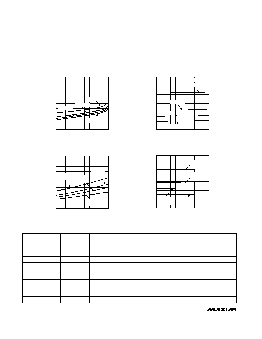
Typical Operating Characteristics
(T
A
= +25°C, unless otherwise noted.)
0
0.4
0.2
1.0
0.8
0.6
1.2
1.4
1.8
1.6
2.0
-40
-10 5
-25
20 35 50 65 80 95 110 125
STANDBY CURRENT vs. TEMPERATURE
MAX7320 toc01
TEMPERATURE (
°C)
STANDBY CURRENT (
µ
A)
V+ = +3.3V
V+ = +2.5V
V+ = +5.0V
V+ = +1.71V
f
SCL
= 0kHz
0
20
10
40
30
50
60
-40
-10 5
20
-25
35 50 65 80 95 110 125
SUPPLY CURRENT vs. TEMPERATURE
MAX7320 toc02
TEMPERATURE (
°C)
SUPPLY CURRENT (
µ
A)
V+ = +3.3V
V+ = +1.71V
V+ = +2.5V
f
SCL
= 400kHz
V+ = +5.0V
OUTPUT VOLTAGE LOW
vs. TEMPERATURE
TEMPERATURE (
°C)
OUTPUT VOLTAGE LOW (V)
MAX7320 toc03
-40 -25 -10 5
20 35 50 65 80 95 110 125
0
0.05
0.10
0.15
0.20
0.25
0.30
0.35
0.40
0.45
0.50
V+ = +3.3V
I
SINK
= 3mA
V+ = +5.0V
I
SINK
= 5mA
V+ = +2.5V
I
SINK
= 2mA
V+ = +1.71V
I
SINK
= 1mA
OUTPUT VOLTAGE HIGH
vs. TEMPERATURE
TEMPERATURE (
°C)
OUTPUT VOLTAGE HIGH (V)
MAX7320 toc04
-40 -25 -10 5
20 35 50 65 80 95 110 125
0
1
2
3
4
5
6
V+ = +5.0V
I
SOURCE
= 5mA
V+ = +3.3V
I
SOURCE
= 3mA
V+ = +1.71V
I
SOURCE
= 1mA
V+ = +2.5V
I
SOURCE
= 2mA
Pin Description
PIN
QSOP
TQFN
NAME
FUNCTION
1, 3
15, 1
AD0, AD2
Address Inputs. Select device slave address with AD0 and AD2. Connect AD0 and AD2
to either GND, V+, SCL, or SDA to give four logic combinations (see Table 3).
2
16
RST
Reset Input, Active Low. Drive RST low to clear the 2-wire interface.
47, 912
25, 710
O0O7
Output Ports. O0 to O7 are push-pull outputs.
8
6
GND
Ground
13
11
N.C.
No Connection. Not internally connected.
14
12
SCL
I
2
C-Compatible Serial Clock Input
15
13
SDA
I
2
C-Compatible Serial Data I/O
16
14
V+
Positive Supply Voltage. Bypass V+ to GND with a 0.047µF ceramic capacitor.
--
EP
EP
Exposed Pad. Connect exposed pad to GND.

Detailed Description
MAX7319MAX7329 Family Comparison
The MAX7319MAX7323 family consists of five pin-
compatible, eight-port expanders. Each version is opti-
mized for different applications. The MAX7328 and
MAX7329 are second sources to the PCF8574 and
PCF8574A.
The MAX7324MAX7327 family consists of four pin-
compatible, 16-port expanders that integrate the func-
tions of the MAX7320 and one of either the MAX7319,
MAX7321, MAX7322, or MAX7323.
Functional Overview
The MAX7320 is a general-purpose port expander
operating from a +1.71V to +5.5V supply that provides
eight push-pull output ports. The MAX7320 is rated to
sink a total of 100mA and source a total of 50mA from
all eight combined outputs.
The MAX7320 is set to one of 16 I
2
C slave addresses
(0x50 to 0x5F) using address select inputs AD0 and AD2,
and is accessed over an I
2
C serial interface up to
400kHz. Note the MAX7320 offers a different range of I
2
C
slave addresses than the MAX7319, MAX7321,
MAX7322, and MAX7323 (these expanders use the
address range 0x60 to 0x6F).
MAX7320
I
2
C Port Expander with Eight Push-Pull Outputs
_______________________________________________________________________________________
5
PART
I
2
C
SLAVE
ADDRESS
INPUTS
INPUT
INTERRUPT
MASK
OPEN-
DRAIN
OUTPUTS
PUSH-
PULL
OUTPUTS
APPLICATION
8-PORT EXPANDERS
MAX7319
110xxxx
8
Yes
--
--
Input-only versions:
Eight input ports with programmable latching
transition detection interrupt and selectable pullups.
Offers maximum versatility for automatic input
monitoring. An interrupt mask selects which inputs
cause an interrupt on transitions, and transition flags
identify which inputs have changed (even
momentarily) since the ports were last read.
MAX7320
101xxxx
--
--
--
8
Output-only versions:
Eight push-pull outputs with selectable power-up
default states.
Push-pull outputs offer faster rise time than open-
drain outputs, and require no pullup resistors.
MAX7321
110xxxx
Up to 8
--
Up to 8
--
I/O versions:
Eight open-drain I/O ports with latching transition
detection interrupt and selectable pullups.
Open-drain outputs can level shift the logic-high
state to a higher or lower voltage than V+ using
external pullup resistors. Any port can be used as an
input by setting the open-drain output to logic-high.
Transition flags identify which inputs have changed
(even momentarily) since the ports were last read.
MAX7322
110xxxx
4
Yes
--
4
Four input-only, four output-only versions:
Four input ports with programmable latching
transition detection interrupt and selectable pullups.
Four push-pull outputs with selectable power-up
default levels.
Table 1. MAX7319MAX7329 Family Comparison