
General Description
The MAX6806/MAX6807/MAX6808 precision voltage
detectors are ideal for accurate monitoring of power
supplies in digital systems. They provide circuit reliabili-
ty and reduce total cost by eliminating external compo-
nents and adjustments.
The MAX6806/MAX6807/MAX6808 assert a reset signal
whenever the supply voltage (V
CC
) falls below the factory-
preset, ±2% accurate threshold. Internal hysteresis
ensures stable switching. The MAX6806/MAX6807/
MAX6808 are available in 4.6V and 2.6V thresholds (2.3V
is also available for the MAX6806 only). The MAX6806 fea-
tures an active-low, push-pull RESET output; the MAX6807
features an active-high, push-pull RESET output; and the
MAX6808 features an active-low, open-drain RESET out-
put. RESET is valid for V
CC
down to 1V (MAX6806/
MAX6808), and RESET (MAX6807) is guaranteed for V
CC
down to 1.2V.
The MAX6806/MAX6807/MAX6808 are available in
3-pin SC70, 3-pin SOT23, and 4-pin SOT143 packages.
The SOT143 package includes a manual-reset input.
Applications
Computers
Controllers
Intelligent Instruments
Critical µP and µC Power Monitoring
Portable/Battery-Powered Equipment
Automotive
Bar-Code Scanners
Features
o
Preset Reset Thresholds: 4.6V and 2.6V
(2.3V also available for MAX6806 only)
o
±2% Accurate Reset Thresholds
o
Reset Output Available in Active-Low (MAX6806),
Active-High (MAX6807), and Open-Drain
(MAX6808) Versions
o
Immune to Power-Supply Transients
o
RESET
Valid to V
CC
= 1.0V (MAX6806/MAX6808)
o
35µA Supply Current
o
No External Components
o
Manual Reset Available with 4-Pin SOT143
Package
o
Miniature 3-Pin SC70, 3-Pin SOT23, and 4-Pin
SOT143 Packages
For free samples & the latest literature: http://www.maxim-ic.com, or phone 1-800-998-8800.
For small orders, phone 1-800-835-8769.
MAX6806/MAX6807/MAX6808
Voltage Detectors
________________________________________________________________
Maxim Integrated Products
1
19-1421; Rev 1; 4/99
PART
RESET OUTPUT
Selector Guide
Ordering Information
TOP MARK
NOMINAL
V
TH-
(V)
MAX6806
UR46-T
MAX6806UR26-T
Active-Low, Push-Pull
FZDP
FZDQ
4.6
2.6
MAX6806UR23-T
MAX6806US46-T
FZDR
KABT
2.3
4.6
MAX6806US26-T
MAX6806US23-T
KABU
KABV
2.6
2.3
Other reset thresholds may be available. Contact factory for availability.
TEMP. RANGE
MAX6806
XR_ _-T
-40°C to +85°C
PART
Typical Operating Circuit and Pin Configurations appear at
end of data sheet.
PIN-PACKAGE
3 SC70
MAX6806US_ _-T
-40°C to +85°C
4 SOT143
MAX6807US_ _-T
-40°C to +85°C
4 SOT143
MAX6807
XR_ _-T
-40°C to +85°C
3 SC70
MAX6808US_ _-T
-40°C to +85°C
4 SOT143
MAX6808
XR_ _-T
-40°C to +85°C
3 SC70
*
All devices available in tape-and-reel only, 2500 piece mini-
mum order quantity.
Note:
Insert the desired number from the Selector Guide into the
blank to complete the part number. Also see Selector Guide for
top mark.
Selector Guide continued at end of data sheet.
MAX6806UR_ _-T
-40°C to +85°C
3 SOT23
MAX6807UR_ _-T
-40°C to +85°C
3 SOT23
MAX6808UR_ _-T
-40°C to +85°C
3 SOT23
MAX6806/MAX6807/MAX6808
Voltage Detectors
2
_______________________________________________________________________________________
ABSOLUTE MAXIMUM RATINGS
ELECTRICAL CHARACTERISTICS
(V
CC
= +5V, T
A
= -40°C to +85°C, unless otherwise noted. Typical values are at T
A
= +25°C.) (Note 1)
Stresses beyond those listed under "Absolute Maximum Ratings" may cause permanent damage to the device. These are stress ratings only, and functional
operation of the device at these or any other conditions beyond those indicated in the operational sections of the specifications is not implied. Exposure to
absolute maximum rating conditions for extended periods may affect device reliability.
Note1:
All devices are 100% production tested at T
A
= +25°C, and are guaranteed by design for T
A
= T
MIN
to T
MAX
, as specified.
Note 2:
RESET output for MAX6806/MAX6808, RESET output for MAX6807.
V
CC
to GND ..........................................................-0.3V to +6.0V
RESET, RESET to GND
(MAX6806/MAX6807) ................................-0.3V to (V
CC
+ 0.3V)
RESET to GND (MAX6808)...................................-0.3V to + 6.0V
MR to GND (SOT143 package only) ....................-0.3V to + 6.0V
Input Current, V
CC
...........................................................±20mA
Output Current, RESET, RESET .......................................±20mA
Rate of Rise, V
CC
...........................................................100V/µs
Continuous Power Dissipation (T
A
= +70°C)
SOT23, SOT143 (derate 4mW/°C above +70°C) .........320mW
SC70 (derate 2.17mW/°C above +70°C) .....................174mW
Operating Temperature Range ..........................-40°C to +85°C
Storage Temperature Range .............................-65°C to +160°C
Lead Temperature (soldering, 10sec) .............................+300°C
V
CC
= +3.6V, no load
V
CC
> V
TH+
T
A
= -40°C to +85°C
T
A
= 0°C to +70°C
V
CC
falling at 1mV/µs
I
SINK
= 1.0mA, V
CC
= 2.0V
I
SINK
= 3.2mA, V
CC
= 5.0V
I
SOURCE
= 400µA, V
CC
= 2.0V
I
SINK
= 20µA, V
CC
= 1.0V
T
A
= +25°C, Figure 2
V
CC
= +5.5V, no load
I
SOURCE
= 20µA, V
CC
= 1.2V
T
A
= +25°C,
V
CC
falling
CONDITIONS
V
0.7V
CC
V
IH
MR Input Threshold
0.6
V
IL
k
40
80
120
R
MR
MR Pull-Down Resistance
ppm/°C
30
Reset Threshold Tempco
µs
30
V
CC
to Reset Delay (Note 2)
0.4
V
OL
RESET Output Voltage
(MAX6807)
V
0.8V
CC
V
OH
0.8V
CC
35
60
V
1.2
5.5
V
CC
1.0
5.5
Supply Voltage Range
V
OL
0.4
0.3
V
0.02
0.03
V
TH-
V
TH-
V
HYST
Reset Threshold Hysteresis
µA
50
80
I
CC
Supply Current
4.508
4.60
4.692
2.548
2.60
2.652
V
2.254
2.30
2.346
V
TH-
Reset Threshold
UNITS
MIN
TYP
MAX
SYMBOL
PARAMETER
MAX680_ _ _46
MAX680_ _ _26
MAX680_ _ _23
V
OH
I
SOURCE
= 2.0mA, V
CC
= 5.0V
(MAX6806 only)
RESET Output Voltage
(MAX6806/MAX6808)
V
0.8V
CC
V
CC
= 5.5V, RESET deasserted
(MAX6808 only)
µA
I
OH
RESET Output Leakage Current
MAX6806/MAX6807/MAX6808
Voltage Detectors
_______________________________________________________________________________________
3
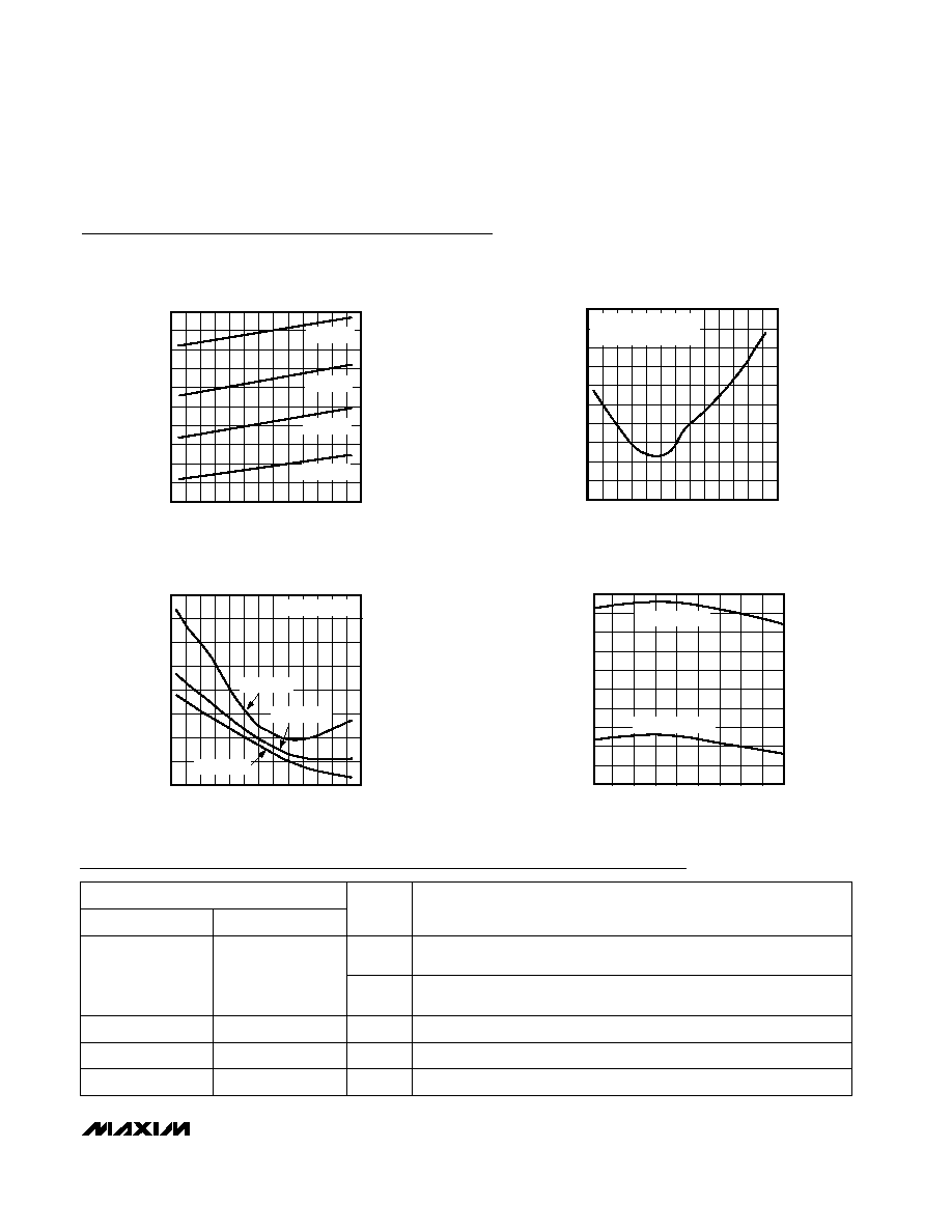
Typical Operating Characteristics
(T
A
= +25°C, unless otherwise noted.)
0
10
5
20
15
30
25
35
45
40
50
-60
-30
0
30
60
120
90
SUPPLY CURRENT vs. TEMPERATURE
MAX6806/7/8-01
TEMPERATURE (°C)
SUPPLY CURRENT (
µ
A)
V
CC
= 5.0V
V
CC
= 3.3V
V
CC
= 1.8V
V
CC
= 1.0V
25
29
27
33
31
35
37
43
41
39
45
-60
-30-15 0
-45
15 30 45
75
60
90 105 120135
POWER-DOWN RESET DELAY
vs. TEMPERATURE
MAX6806/7/8toc02
TEMPERATURE (°C)
RESET DELAY (
µ
s)
V
OD
= V
TH-
- V
CC
= 100mV
V
CC
FALLING AT 1mV/
µ
S
4
6
5
7
9
8
11
10
12
-60
-30
0
30
60
120
90
POWER-UP RESET DELAY vs. TEMPERATURE
MAX6806/7/8-03
TEMPERATURE (°C)
DELAY TIME (
µ
s)
V
OD
= V
CC
- V
TH
+
V
OD
= 50mV
V
OD
= 200mV
V
OD
= 100mV
0.9900
0.9940
0.9920
0.9980
0.9960
1.0020
1.0000
1.0040
1.0080
1.0060
1.0100
-40
-15
0
-30
15
30
60
45
85
75
NORMALIZED RESET THRESHOLD
vs. TEMPERATURE
MAX6806/7/8-04
TEMPERATURE (°C)
NORMALIZED RESET THRESHOLD
V
CC
RISING (V
TH+
)
V
CC
FALLING (V
TH-
)
1
Active-Low Reset Output (MAX6806/MAX6808). RESET remains low
while V
CC
is below the reset-threshold voltage or while MR is held high.
Active-High Reset Output (MAX6807). RESET remains high while V
CC
is
below the reset-threshold voltage or while MR is held high.
2
Ground
3
Supply Voltage Input
--
Active-High Manual Reset Input. Internal 80k
resistor to GND.
SOT23/SC70
FUNCTION
Pin Description
RESET
RESET
GND
V
CC
MR
NAME
1
4
3
2
SOT143
PIN
MAX6806/MAX6807/MAX6808
Voltage Detectors
4
_______________________________________________________________________________________
_______________Detailed Description
Reset Output
The MAX6806 voltage detector features an active-low,
push-pull RESET output, while the MAX6807 features
an active-high, push-pull RESET output. Unlike micro-
processor (µP) supervisory circuits that offer a reset
timeout period, the MAX6806 and MAX6807 RESET
goes high and RESET goes low virtually immediately
once V
CC
exceeds the reset threshold. If a brownout
occurs (V
CC
falls below the reset threshold), RESET
goes low and RESET goes high. RESET is guaranteed
to be a logic low for V
CC
1V and RESET is guaran-
teed to be a logic high for V
CC
1.2V.
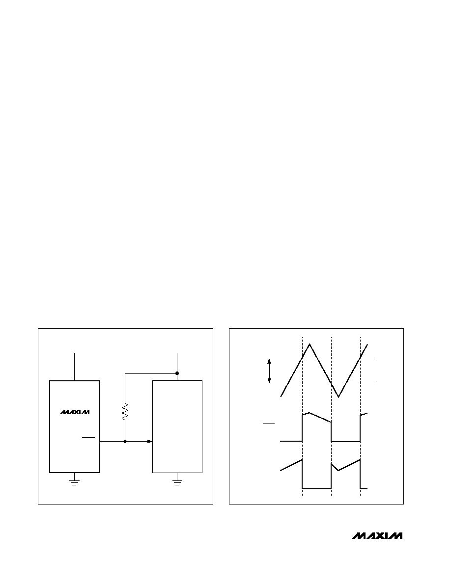
The MAX6808 features an active-low, open-drain RESET
output. The output sinks current when V
CC
falls below
the reset threshold. Connect a pull-up resistor from
RESET to any supply voltage up to 6V (Figure 1). Select
a resistor value large enough to provide a logic low and
small enough to provide a logic high while supplying all
input and leakage currents connected to the RESET
line. A 100k
resistor is sufficient in applications driving
high-impedance loads.
The manual reset input (MR, 4-pin SOT143 package)
can also initiate a reset (see
Manual Reset Input sec-
tion).
Manual Reset Input
Many applications require manual-reset capabilities,
allowing an operator, a test technician, or external logic
circuitry to initiate a reset. A logic high on MR asserts a
reset and remains asserted while MR is high. This input
has an 80k
pull-down resistor, so the input may be left
unconnected if not used. Connect a normally open
momentary switch from MR to V
CC
to create a manual-
reset function. If MR is driven from long cables or if the
device is used in a noisy environment, connecting a
0.1µF capacitor from MR to ground provides noise
immunity.
Hysteresis
The MAX6806/MAX6807/MAX6808 feature internal hys-
teresis that creates two trip points: one for the rising
supply voltage and one for the falling supply voltage
(Figure 2). The hysteresis prevents the output from oscil-
lating (chattering) when V
CC
is near the reset threshold.
Reset Threshold Accuracy
The MAX6806/MAX6807/MAX6808 are ideal for sys-
tems using a 5V ±5%, 3V ±5%, or 2.5V ±5% power
supply with ICs specified for 5V ±10%, 3V ±10%, or
2.5V ±10%, respectively. The reset is guaranteed to
assert after the power supply falls out of regulation, but
before power drops below the minimum specified oper-
ating voltage range for the system ICs.
MAX6808
V
CC
V
CC
GND
+3.3V
GND
+5.0V
100k
5V SYSTEM
RESET
Figure 1. The MAX6808 open-drain RESET output allows use
with multiple supplies.
V
TH+
HYST
RESET
(MAX6806/MAX6808)
RESET
(MAX6807)
V
HYST
= V
TH+
- V
TH-
V
OH
V
OL
V
OH
V
OL
V
TH-
Figure 2. Input and Output Waveforms with V
CC
Varied
Applications Information
Negative-Going V
CC
Transients
In addition to asserting a reset signal during power-up,
power-down, and brown-out conditions, the MAX6806/
MAX6807/MAX6808 are immune to short-duration, neg-
ative-going V
CC
transients.
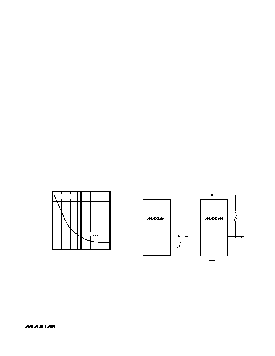
Figure 3 displays typical transient durations vs. reset-
comparator overdrive for which the MAX6806/MAX6807/
MAX6808 do
not
generate a reset pulse. The graph was
generated using a negative-going pulse applied to V
CC
,
starting 0.5V above the actual reset threshold and end-
ing below it by the magnitude indicated (reset-compara-
tor overdrive). The graph indicates the maximum pulse
width a negative-going V
CC
transient can have without
causing a reset pulse. As the magnitude of the transient
increases (goes further below the reset threshold), the
maximum allowable pulse width decreases. A 0.1µF
capacitor mounted as close as possible to V
CC
pro-
vides additional transient immunity.
Ensuring a Valid Reset Output Down to
V
CC
= Ground
When V
CC
falls below 1V, the MAX6806/MAX6808
RESET output no longer sinks current--it becomes an
open circuit. Therefore, high-impedance CMOS logic
inputs connected to RESET can drift to undetermined
voltages. This presents no problem in most applica-
tions, since most circuitry is inoperative when V
CC
is
below 1V. In applications where RESET must be valid
down to ground, add a pull-down resistor to RESET so
any stray leakage currents flow to ground, holding
RESET low (Figure 4). Select R1 to be large enough not
to load RESET and small enough to pull RESET to
ground. For most applications, 100k
will not load
RESET and will pull RESET to ground. Similarly, if
RESET (MAX6807) must be valid below 1.2V, add a
pull-up resistor to RESET.
MAX6806/MAX6807/MAX6808
Voltage Detectors
_______________________________________________________________________________________
5
80
70
20
10
100
1000
40
30
50
60
RESET COMPARATOR OVERDRIVE, V
TH-
- V
CC
(mV)
MAXIMUM TRANSIENT DURATION (
µ
s)
T
A
= +25°C
MAX680 46
Figure 3. Maximum Transient Duration without Causing a
Reset Pulse vs. Reset Comparator Overdrive
MAX6806
MAX6807
V
CC
V
CC
GND
GND
RESET
RESET
R1
100k
R1
100k
Figure 4. RESET / RESET Valid to V
CC
= Ground Circuit