_______________General Description
The MAX662A is a regulated +12V, 30mA-output, charge-
pump DC-DC converter. It provides the necessary +12V
▒5% output to program byte-wide flash memories, and
requires no inductors to deliver a guaranteed 30mA out-
put from inputs as low as 4.75V. It fits into less than 0.1in
2
of board space. The MAX662A is a pin-compatible
upgrade to the MAX662, and is recommended for new
designs. The MAX662A offers lower quiescent and shut-
down currents, and guarantees the output current over all
temperature ranges.
The MAX662A is the first charge-pump boost converter to
provide a regulated +12V output. It requires only a few
inexpensive capacitors, and the entire circuit is complete-
ly surface-mountable.
A logic-controlled shutdown pin that interfaces directly
with microprocessors reduces the supply current to only
0.5ÁA. The MAX662A comes in 8-pin narrow SO and DIP
packages.
For higher-current flash memory programming solutions,
refer to the data sheets for the MAX734 (120mA output
current, guaranteed) and MAX732 (200mA output cur-
rent, guaranteed) PWM, switch-mode DC-DC converters.
Or, refer to the MAX761 data sheet for a 150mA, PFM
switch-mode DC-DC converter that operates from inputs
as low as 2V.
________________________Applications
+12V Flash Memory Programming Supplies
Compact +12V Op-Amp Supplies
Switching MOSFETs in Low-Voltage Systems
Dual-Output +12V and +20V Supplies
____________________________Features
o
Regulated +12V ▒5% Output Voltage
o
4.5V to 5.5V Supply Voltage Range
o
Fits in 0.1in
2
o
Guaranteed 30mA Output
o
No Inductor--Uses Only 4 Capacitors
o
185ÁA Quiescent Current
o
Logic-Controlled 0.5ÁA Shutdown
o
8-Pin Narrow SO and DIP Packages
______________Ordering Information
MAX662A
+12V, 30mA Flash Memory
Programming Supply
________________________________________________________________
Maxim Integrated Products
1
1
2
3
4
8
7
6
5
SHDN
GND
V
OUT
V
CC
C2+
C2-
C1+
C1-
MAX662A
DIP/SO
TOP VIEW
__________________Pin Configuration
MAX662A
FLASH
MEMORY
4.7
Á
F
4.7
Á
F
0.22
Á
F
0.22
Á
F
OUTPUT
12V ▒5%
30mA
V
CC
SHDN
C1+
C1-
V
OUT
C2-
C2+
GND
INPUT
4.75V TO 5.5V
V
pp
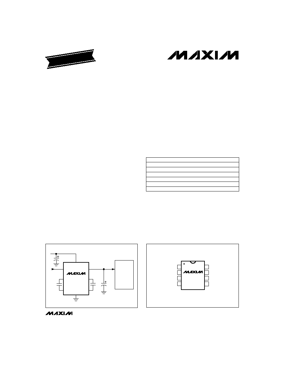
__________Typical Operating Circuit
Call toll free 1-800-998-8800 for free samples or literature.
19-0253; Rev 1; 8/94
EVALUATION KIT MANUAL
FOLLOWS DATA SHEET
PART
MAX662ACPA
MAX662ACSA
MAX662AC/D
0░C to +70░C
0░C to +70░C
0░C to +70░C
TEMP. RANGE
PIN-PACKAGE
8 Plastic DIP
8 SO
Dice*
MAX662AEPA
-40░C to +85░C
8 Plastic DIP
MAX662AESA
-40░C to +85░C
8 SO
MAX662AMJA
-55░C to +125░C
8 CERDIP**
* Dice are tested at T
A
= +25░C.
** Contact factory for availability and processing to MIL-STD-883.

MAX662A
+12V, 30mA Flash Memory
Programming Supply
2
_______________________________________________________________________________________
ABSOLUTE MAXIMUM RATINGS
ELECTRICAL CHARACTERISTICS
(Circuit of Figure 3a, V
CC
= 4.5V to 5.5V, T
A
= T
MIN
to T
MAX
, unless otherwise noted.)
Stresses beyond those listed under "Absolute Maximum Ratings" may cause permanent damage to the device. These are stress ratings only, and functional
operation of the device at these or any other conditions beyond those indicated in the operational sections of the specifications is not implied. Exposure to
absolute maximum rating conditions for extended periods may affect device reliability.
V
CC
to GND ................................................................-0.3V to 6V
SHDN..........................................................-0.3V to (V
CC
+ 0.3V)
I
OUT
Continuous..................................................................50mA
Continuous Power Dissipation (T
A
= +70░C)
Plastic DIP (derate 9.09mW/░C above +70░C) ............727mW
SO (derate 5.88mW/░C above +70░C) .........................471mW
CERDIP (derate 8.00mW/░C above +70░C) .................640mW
Operating Temperature Ranges
MAX662AC_A .....................................................0░C to +70░C
MAX662AE_A ..................................................-40░C to +85░C
MAX662AMJA................................................-55░C to +125░C
Storage Temperature Range .............................-65░C to +160░C
Lead Temperature (soldering, 10sec) .............................+300░C
MAX662AC/E
V
CC
= V
SHDN
= 5V,
I
OUT
= 30mA
V
CC
= 5V, I
OUT
= 30mA
MAX662AM
No load, V
SHDN
= 0V
No load, V
SHDN
= V
CC
V
CC
= V
SHDN
= 5V
V
CC
= 5V, I
OUT
= 30mA
V
CC
= 5V, V
SHDN
= 0V
CONDITIONS
ÁA
0
SHDN Pin Current
-50
-15
-5
11.4
12
12.6
11.4
12
12.6
11.4
12
12.6
V
0.4
V
IL
Shutdown Input Threshold
2.4
V
IH
k
1
2
R
SW
V
CC
-to-V
OUT
Switch Impedance
%
76
Power Efficiency
V
11.4
12
12.6
V
OUT
Output Voltage
ÁA
185
500
I
CC
Supply Current
ÁA
0.5
10
Shutdown Current
kHz
500
f
OSC
Oscillator Frequency
UNITS
MIN
TYP
MAX
SYMBOL
PARAMETER
__________________________________________Typical Operating Characteristics
(Circuit of Figure 3a, T
A
= +25░C, unless otherwise noted.)
100
4.50
5.25
SUPPLY CURRENT vs. SUPPLY VOLTAGE
140
300
MAX662A-01
SUPPLY VOLTAGE (V)
SUPPLY CURRENT (
Á
A)
220
180
4.75
260
5.00
120
160
200
240
280
5.50
T
A
= -55░C
T
A
= 0░C
T
A
= +25░C
T
A
= +125░C
12.6
10.6
0
20
60
100
OUTPUT VOLTAGE vs. OUTPUT CURRENT
11.0
12.2
MAX662A-02
OUTPUT CURRENT (mA)
OUTPUT VOLTAGE (V)
40
80
11.8
11.4
10
30
50
70
90
10.8
11.2
11.6
12.0
12.4
V
CC
= 5.5V
V
CC
= 5.0V
V
CC
= 4.75V
V
CC
= 4.5V
CONTINUOUS OUTPUT CURRENT MUST
NOT EXCEED 50mA ABS MAX LIMIT.
INTERMITTENT PEAK CURRENTS MAY
BE HIGHER.
30
0
20
60
100
EFFICIENCY vs. LOAD CURRENT
50
MAX662A-03
LOAD CURRENT (mA)
EFFICIENCY (%)
40
80
90
70
10
30
50
70
90
40
60
80
100
V
CC
= 5.5V
V
CC
= 5.0V
V
CC
= 4.75V
V
CC
= 4.5V
CONTINUOUS OUTPUT CURRENT
MUST NOT EXCEED 50mA ABS MAX
LIMIT. INTERMITTENT PEAK
CURRENTS MAY BE HIGHER.
0mA
I
OUT
30mA,
V
CC
= 4.75V to 5.5V
0mA
I
OUT
20mA
0mA
I
OUT
24mA,
V
CC
= 4.75V to 5.5V
0mA
I
OUT
16mA
MAX662AC/E
MAX662AM
1
2.5

MAX662A
+12V, 30mA Flash Memory
Programming Supply
_______________________________________________________________________________________
3
LOAD-TRANSIENT RESPONSE
A: OUTPUT CURRENT, 20mA/div, I
OUT
= 0mA to 30mA
B: OUTPUT VOLTAGE RIPPLE, 100mV/div, V
CC
= 5.0V
1ms/div
A
B
0mA
_____________________________Typical Operating Characteristics (continued)
(Circuit of Figure 3a, T
A
= +25░C, unless otherwise noted.)
LINE-TRANSIENT RESPONSE
A: SUPPLY VOLTAGE, 2V/div, V
CC
= 4.5V to 5.5V, I
OUT
= 30mA
B: OUTPUT VOLTAGE RIPPLE, 200mV/div
1ms/div
A
B
0V
0V
_____________________Pin Description
NAME
FUNCTION
1
C1-
Negative terminal for the first charge-
pump capacitor
PIN
2
C1+
Positive terminal for the first charge-
pump capacitor
4
C2+
Positive terminal for the second
charge-pump capacitor
3
C2-
Negative terminal for the second
charge-pump capacitor
7
GND
Ground
6
V
OUT
+12V Output Voltage. V
OUT
= V
CC
when in shutdown mode.
5
V
CC
Supply Voltage
8
Active-high CMOS-logic level
Shutdown Input. SHDN is internally
pulled up to V
CC
. Connect to GND for
normal operation. In shutdown mode,
the charge pumps are turned off and
V
OUT
= V
CC
.
SHDN
MAX662A
C1-
C1+
C2-
C2+
C4
4.7
Á
F
0.22
Á
F
0.22
Á
F
V
CC
V
CC
S1
S2
S1
S1
S1
S2
S2
GND
OSCILLATOR
VREF
R1
R2
SHDN
V
OUT
C5
4.7
Á
F
C3*
0.1
Á
F
+12V
SWITCH CLOSURES SHOWN FOR CHARGE PUMP IN THE TRANSFER MODE
* C3 NOT REQUIRED. FOR MAX662 ONLY.
ERROR
AMP
Figure 1. Block Diagram
MAX662A
_______________Detailed Description
Operating Principle
The MAX662A provides a regulated 12V output voltage
at 30mA from a 5V ▒5% power supply, making it ideal
for flash EEPROM programming applications. It uses
internal charge pumps and external capacitors to gen-
erate +12V, eliminating inductors. Regulation is provid-
ed by a pulse-skipping scheme that monitors the
output voltage level and turns on the charge pumps
when the output voltage begins to droop.
Figure 1 shows a simplified block diagram of the
MAX662A. When the S1 switches are closed and the
S2 switches are open, capacitors C1 and C2 are
charged up to V
CC
. The S1 switches are then opened
and the S2 switches are closed so that capacitors C1
and C2 are connected in series between V
CC
and
V
OUT
. This performs a voltage tripling function. A pulse-
skipping feedback scheme adjusts the output voltage
to 12V ▒5%. The efficiency of the MAX662A with V
CC
=
5V and I
OUT
= 30mA is typically 76%. See the
Efficiency vs. Load Current graph in the
Typical
Operating Characteristics.
During one oscillator cycle, energy is transferred from
the charge-pump capacitors to the output filter capaci-
tor and the load. The number of cycles within a given
time frame increases as the load current increases or
as the input supply voltage decreases. In the limiting
case, the charge pumps operate continuously, and the
oscillator frequency is nominally 500kHz.
Shutdown Mode
The MAX662A enters shutdown mode when SHDN is a
logic high. SHDN is a TTL/CMOS-compatible input sig-
nal that is internally pulled up to V
CC
. In shutdown
mode, the charge-pump switching action is halted and
V
IN
is connected to V
OUT
through a 1k
switch. When
entering shutdown, V
OUT
declines to V
CC
in typically
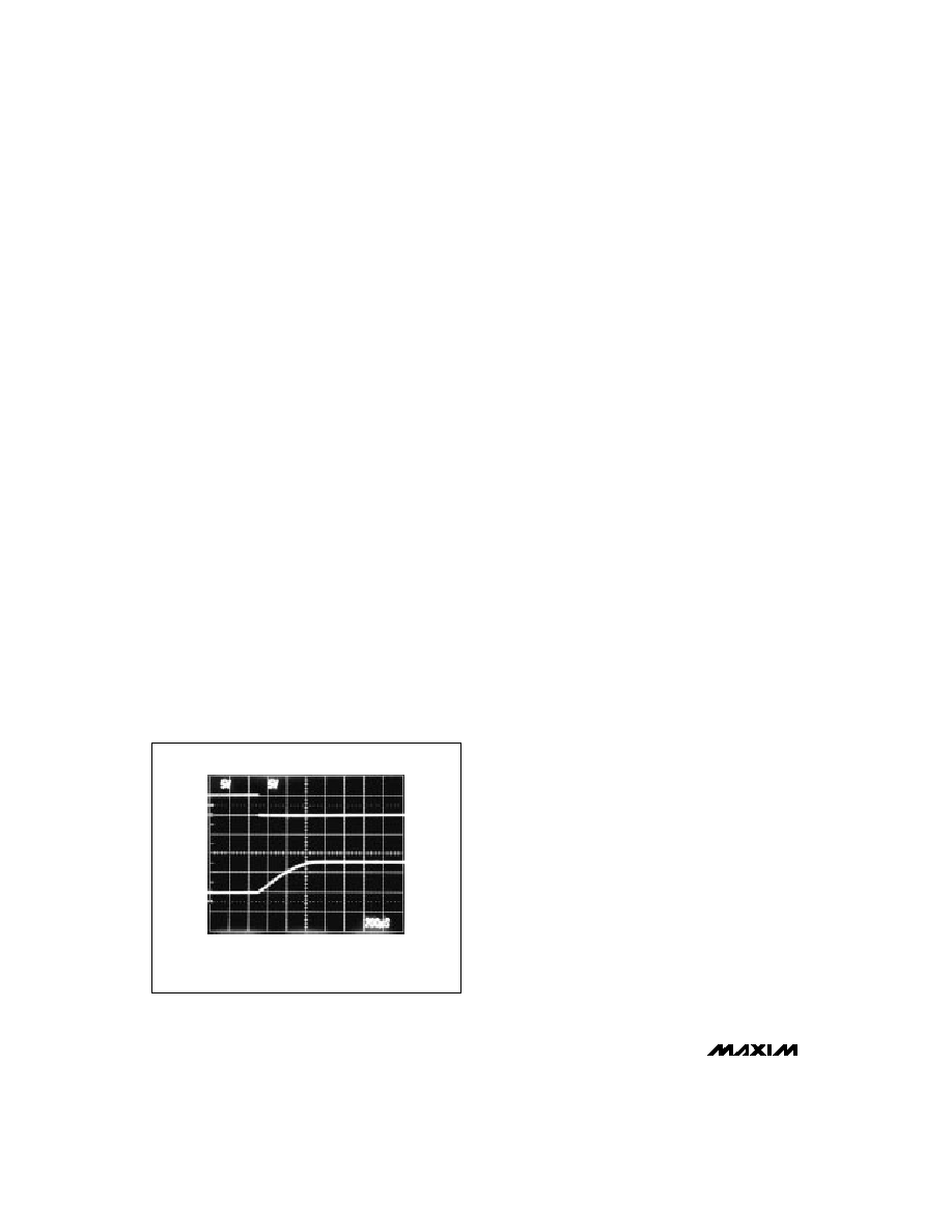
13ms. Connect SHDN to ground for normal operation.
When V
CC
= 5V, it takes typically 400Ás for the output
to reach 12V after SHDN goes low (Figure 2).
__________Applications Information
Compatibility with MAX662
The MAX662A is a 100%-compatible upgrade of the
MAX662. The MAX662A does not require capacitor C3,
although its presence does not affect performance.
Capacitor Selection
Charge-Pump Capacitors, C1 and C2
The capacitance values of the charge-pump capacitors
C1 and C2 are critical. Use ceramic or tantalum capaci-
tors in the 0.22ÁF to 1.0ÁF range. For applications requir-
ing operation over extended and/or military temperature
ranges, use 1.0ÁF tantalum capacitors for C1 and C2
(Figure 3b).
Input and Output Capacitors, C4 and C5
The type of input bypass capacitor (C4) and output filter
capacitor (C5) affects performance. Tantalums, ceramics
or aluminum electrolytics are suggested. For smallest size,
use Sprague 595D475X9016A7 surface-mount capacitors,
which are 3.51mm x 1.81mm. For lowest ripple, use low-
ESR through-hole ceramic or tantalum capacitors. For low-
est cost, use aluminum electrolytic or tantalum capacitors.
Figure 3a shows the component values for proper opera-
tion over the commercial temperature range using mini-
mum board space. The input bypass capacitor (C4) and
output filter capacitor (C5) should both be at least 4.7ÁF
when using Sprague's miniature 595D series of tantalum
chip capacitors. Figure 3b shows the suggested compo-
nent values for applications over extended and/or mili-
tary temperature ranges.
The values of C4 and C5 can be reduced to 2ÁF and
1ÁF, respectively, when using ceramic capacitors. If
using aluminum electrolytics, choose capacitance values
of 10ÁF or larger for C4 and C5. Note that as V
CC
increases above 5V and the output current decreases,
the amount of ripple at V
OUT
increases due to the slower
oscillator frequency combined with the higher input volt-
age. Increase the input and output bypass capacitance
to reduce output ripple.
Table 1 lists various capacitor suppliers.
+12V, 30mA Flash Memory
Programming Supply
4
_______________________________________________________________________________________
Figure 2. MAX662A Exiting Shutdown
CIRCUIT OF FIGURE 3, V
CC
= 5V, I
OUT
= 200ÁA
5V
0V
12V
5V
SHDN
V
OUT
200Ás/div

Layout Considerations
Layout is critical, due to the MAX662A's high oscillator
frequency. Good layout ensures stability and helps
maintain the output voltage under heavy loads. For best
performance, use very short connections to the capaci-
tors. The order of importance is: C4, C5, C1, C2.
Flash EEPROM Applications
The circuit of Figure 3a is a +12V ▒5% 30mA flash
EEPROM programming power supply. A microproces-
sor controls the programming voltage via the SHDN
pin. When SHDN is low, the output voltage (which is
connected to the flash memory V
PP
supply-voltage pin)
rises to +12V to facilitate programming the flash memo-
ry. When SHDN is high, the output voltage is connected
to V
IN
through an internal 1k
resistor.
Paralleling Devices
Two MAX662As can be placed in parallel to increase
output drive capability. The V
CC
, V
OUT
, and GND pins
can be paralleled, reducing pin count. Use a single
bypass capacitor and a single output filter capacitor
with twice the capacitance value if the two devices can
be placed close to each other. If the MAX662As cannot
be placed close together, use separate bypass and
output capacitors. The amount of output ripple
observed will determine whether single input bypass
and output filter capacitors can be used. Under certain
conditions, one device may supply the total output cur-
rent. Therefore, regardless of the number of devices in
parallel, the maximum continuous current must not
exceed 50mA.
12V and 20V Dual-Output Power Supply
Using the charge-pump voltage-doubler circuit of
Figure 4, the MAX662A can produce a +20V supply
from a single +5V supply. Figure 5 shows the current
capability of the +20V supply.
MAX662A
+12V, 30mA Flash Memory
Programming Supply
_______________________________________________________________________________________
5
Table 1. Capacitor Suppliers
MAX662A
*C1
1.0
Á
F
2
1
8
7
C2-
C2+
V
CC
V
OUT
PROGRAMMING
CONTROL
DIRECT FROM
Á
P
*C2
1.0
Á
F
V
IN
4.75V TO 5.5V
*C4
22
Á
F
V
OUT
+12V ▒5%
AT 30mA
*C5
22
Á
F
C1+
C1-
SHDN
GND
3
4
5
6
*SPRAGUE 595D SERIES OR EQUIVALENT
MAX662A
C1
0.22
Á
F
2
1
8
7
C2-
C2+
V
CC
V
OUT
PROGRAMMING
CONTROL
DIRECT FROM
Á
P
C2
0.22
Á
F
V
IN
4.75V TO 5.5V
C4
4.7
Á
F
V
OUT
+12V ▒5%
AT 30mA
C5
4.7
Á
F
C1+
C1-
SHDN
GND
3
4
5
6
Figure 3a. Flash EEPROM Programming Power Supply for
Commercial Temperature Range Applications
Figure 3b. Flash EEPROM Programming Power Supply for
Extended and/or Military Temperature Range Applications
Supplier
Phone Number
Fax Number
Capacitor
Capacitor Type*
GRM42-6Z5U224M50
0.22ÁF Ceramic (SM)
Murata Erie
(814) 237-1431
(814) 238-0490
RPE123Z5U105M50V
1.0ÁF Ceramic (TH)
595D475X9016A7
4.7ÁF Tantalum (SM)
Sprague Electric
(603) 224-1961
(207) 324-4140
(603) 224-1430
(207) 324-7223
595D105X9016A7
1.0ÁF Tantalum (SM)
*Note: (SM) denotes surface-mount component, (TH) denotes through-hole component.