General Description
The MAX6412¡MAX6420 low-power microprocessor
supervisor circuits monitor system voltages from 1.6V to
5V. These devices are designed to assert a reset signal
whenever the V
CC
supply voltage or RESET IN falls below
its reset threshold or the manual reset input is asserted.
The reset output remains asserted for the reset timeout
period after V
CC
and RESET IN rise above the reset
threshold and the manual reset input is deasserted. The
reset timeout is externally set by a capacitor to provide
more flexibility.
The MAX6412/MAX6413/MAX6414 feature fixed thresholds
from 1.575V to 5V in approximately 100mV increments and
a manual reset input. The MAX6415/MAX6416/MAX6417
are offered with an adjustable reset input that can monitor
voltages down to 1.26V and the MAX6418/MAX6419/
MAX6420 are offered with one fixed input and one
adjustable input to monitor dual-voltage systems.
The MAX6412/MAX6415/MAX6418 have an active-low,
push-pull reset output. The MAX6413/MAX6416/
MAX6419 have an active-high, push-pull reset output
and the MAX6414/MAX6417/MAX6420 have an active-
low, open-drain reset output. All of these devices are
offered in a SOT23-5 package and are fully specified
from -40░C to +125░C.
Applications
Automotive
Medical Equipment
Intelligent Instruments
Portable Equipment
Battery-Powered Computers/Controllers
Embedded Controllers
Critical ÁP Monitoring
Set-Top Boxes
Computers
Features
o Monitor System Voltages from 1.6V to 5V
o Capacitor-Adjustable Reset Timeout Period
o Manual Reset Input (MAX6412/MAX6413/MAX6414)
o Adjustable Reset Input Option
(MAX6415¡MAX6420)
o Dual-Voltage Monitoring
(MAX6418/MAX6419/MAX6420)
o Low Quiescent Current (1.7ÁA, typ)
o 3 RESET Output Options
Push-Pull RESET
Push-Pull RESET
Open-Drain RESET
o Guaranteed Reset Valid to V
CC
= 1V
o Power-Supply Transient Immunity
o Small SOT23-5 Packages
MAX6412¡MAX6420
Low-Power, Single/Dual-Voltage ÁP Reset Circuits
with Capacitor-Adjustable Reset Timeout Delay
________________________________________________________________ Maxim Integrated Products
1
Ordering Information
GND
SRT
1
5
V
CC
MAX6412¡
MAX6420
SOT23-5
TOP VIEW
2
3
4
RESET/RESET
RESET IN (MR)
( ) FOR THE MAX6412/MAX6413/MAX6414.
Pin Configuration
19-2336; Rev 1; 8/03
For pricing, delivery, and ordering information, please contact Maxim/Dallas Direct! at
1-888-629-4642, or visit Maxim's website at www.maxim-ic.com.
Typical Operating Circuit appears at end of data sheet.
Selector Guide appears at end of data sheet.
PART
TEMP RANGE
PIN-PACKAGE
MAX6412UK_ _-T
-40░C to +125░C
5 SOT23-5
MAX6413UK_ _-T
-40░C to +125░C
5 SOT23-5
MAX6414UK_ _-T
-40░C to +125░C
5 SOT23-5
MAX6415UK-T
-40░C to +125░C
5 SOT23-5
MAX6416UK-T
-40░C to +125░C
5 SOT23-5
MAX6417UK-T
-40░C to +125░C
5 SOT23-5
MAX6418UK_ _-T
-40░C to +125░C
5 SOT23-5
MAX6419UK_ _-T
-40░C to +125░C
5 SOT23-5
MAX6420UK_ _-T
-40░C to +125░C
5 SOT23-5
Note: The MAX6412/MAX6413/MAX6414 and MAX6418/
MAX6419/MAX6420 are available with factory-set V
CC
reset
thresholds from 1.575V to 5.0V in approximately 0.1V incre-
ments. Insert the desired nominal reset threshold suffix (from
Table 1) into the blanks following the letters UK. There are 33
standard versions with a required order increment of 2500
pieces. Sample stock is generally held on standard versions
only (see Standard Versions Table). Required order increment is
10,000 pieces for nonstandard versions. Contact factory for
availability. All devices are available in tape-and-reel only.

MAX6412¡MAX6420
Low-Power, Single/Dual-Voltage ÁP Reset Circuits
with Capacitor-Adjustable Reset Timeout Delay
2
_______________________________________________________________________________________
ABSOLUTE MAXIMUM RATINGS
ELECTRICAL CHARACTERISTICS
(V
CC
= 1V to 5.5V, T
A
= T
MIN
to T
MAX
, unless otherwise specified. Typical values are at V
CC
= 5V and T
A
= +25░C.) (Note 1)
Stresses beyond those listed under "Absolute Maximum Ratings" may cause permanent damage to the device. These are stress ratings only, and functional
operation of the device at these or any other conditions beyond those indicated in the operational sections of the specifications is not implied. Exposure to
absolute maximum rating conditions for extended periods may affect device reliability.
All Voltages Referenced to GND
V
CC
........................................................................-0.3V to +6.0V
SRT, MR, RESET IN ....................................-0.3V to (V
CC
+ 0.3V)
RESET, RESET (Push-Pull) .........................-0.3V to (V
CC
+ 0.3V)
RESET (Open-Drain) .............................................-0.3V to +6.0V
Input Current (All Pins) .....................................................▒20mA
Output Current (RESET, RESET) ......................................▒20mA
Continuous Power Dissipation (T
A
= +70░C)
5-Pin SOT23-5 (derate 7.1mW/░C above +70░C) ........571mW
Operating Temperature Range .........................-40░C to +125░C
Junction Temperature ......................................................+150░C
Storage Temperature Range .............................-65░C to +150░C
Lead Temperature (soldering, 10s) .................................+300░C
PARAMETER
SYMBOL
CONDITIONS
MIN
TYP
MAX
UNITS
Supply Voltage Range
V
CC
1.0
5.5
V
V
CC
5.0V
2.7
4.5
V
CC
3.3V
2
3.5
Supply Current
I
CC
V
CC
2.0V
1.7
2.5
ÁA
T
A
= +25░C
V
TH
-
1.5%
V
TH
+
1.5%
T
A
= 0░C to +125░C
V
TH
-
2.5%
V
TH
+
2.5%
V
CC
Reset Threshold Accuracy
V
TH
T
A
= -40░C to 0░C
V
TH
-
3.5%
V
TH
+
3.5%
V
Hysteresis
V
HYST
3
V
TH
mV
V
CC
to Reset Delay
t
RD
V
CC
falling at 1mV/Ás
100
Ás
C
SRT
= 1500pF
3.35
4.375
5.40
Reset Timeout Period
t
RP
C
SRT
= 0
0.275
ms
V
SRT
Ramp Current
I
RAMP
V
SRT
= 0 to 0.65V; V
CC
= 1.6V to 5V
240
nA
V
SRT
Ramp Threshold
V
TH-RAMP
V
CC
= 1.6V to 5V (V
RAMP
rising)
0.65
V
RAMP Threshold Hysteresis
V
RAMP
falling threshold
33
mV
V
CC
1.0V, I
SINK
= 50ÁA
0.3
V
CC
2.7V, I
SINK
= 1.2mA
0.3
RESET Output Voltage LOW
V
OL
V
CC
4.5V, I
SINK
= 3.2mA
0.4
V
V
CC
1.8V, I
SOURCE
= 200ÁA
0.8
V
CC
V
CC
2.25V, I
SOURCE
= 500ÁA
0.8
V
CC
RESET Output Voltage HIGH,
(Push-Pull)
V
OH
V
CC
4.5V, I
SOURCE
= 800ÁA
0.8
V
CC
V
RESET Output Leakage Current,
(Open-Drain)
I
LKG
V
CC
> V
TH
, reset not asserted
1.0
ÁA
V
CC
1.0V, I
SOURCE
= 1ÁA
0.8
V
CC
V
CC
1.8V, I
SOURCE
= 150ÁA
0.8
V
CC
V
CC
2.7V, I
SOURCE
= 500ÁA
0.8
V
CC
RESET Output Voltage HIGH
V
OH
V
CC
4.5V, I
SOURCE
= 800ÁA
0.8
V
CC
V

MAX6412¡MAX6420
Low-Power, Single/Dual-Voltage ÁP Reset Circuits
with Capacitor-Adjustable Reset Timeout Delay
_______________________________________________________________________________________
3
ELECTRICAL CHARACTERISTICS (continued)
(V
CC
= 1V to 5.5V, T
A
= T
MIN
to T
MAX
, unless otherwise specified. Typical values are at V
CC
= 5V and T
A
= +25░C.) (Note 1)
PARAMETER
SYMBOL
CONDITIONS
MIN
TYP
MAX
UNITS
V
CC
1.8V, I
SINK
= 500ÁA
0.3
V
CC
2.7V, I
SINK
= 1.2mA
0.3
RESET Output Voltage LOW
V
OL
V
CC
4.5V, I
SINK
= 3.2mA
0.4
V
RESET IN Leakage Current
10
nA
RESET IN Threshold
V
RST
V
RST
falling, V
CC
= 1.6V to 5.0V
1.212
1.263
1.313
V
RESET IN Hysteresis
25
mV
V
IL
0.8
V
IH
V
CC
> 4.0V
2.4
V
IL
0.3
V
CC
MR Input
V
IH
V
CC
< 4.0V
0.7
V
CC
V
MR Minimum Pulse Width
1
Ás
MR Glitch Rejection
75
ns
MR to RESET Delay
50
Ás
MR Pullup Resistance
Pull up to V
CC
12
20
28
k
Note 1: Devices production tested at +25░C. Over temperature limits are guaranteed by design.
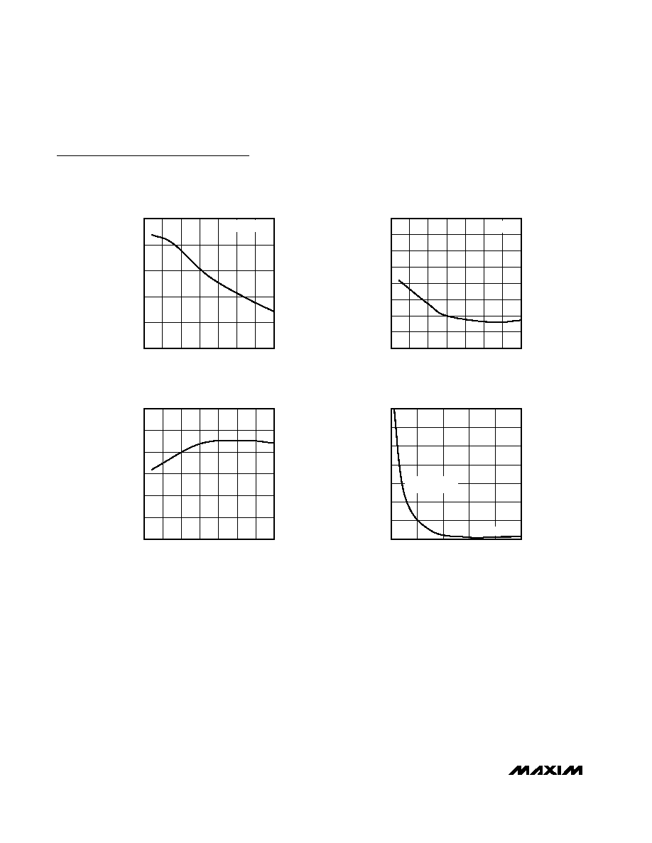
Typical Operating Characteristics
(V
CC
= 5V, C
SRT
= 1500pF, T
A
= +25░C, unless otherwise noted.)
4
3
2
1
0
0
3
1
2
4
5
6
SUPPLY CURRENT vs.
SUPPLY VOLTAGE
MAX6412-20 toc01
SUPPLY VOLTAGE (V)
SUPPLY CURRENT (
Á
A)
T
A
= +125
░C
T
A
= +25
░C
T
A
= -40
░C
0
1.0
0.5
2.0
1.5
3.0
2.5
3.5
-50
0
25
-25
50
75
100
125
SUPPLY CURRENT vs.
TEMPERATURE
MAX6412-20 toc02
TEMPERATURE (
░C)
SUPPLY CURRENT (
Á
A)
V
CC
= 5V
V
CC
= 3.3V
V
CC
= 1.8V
V
CC
= 1V
0.1
1
100
10
1000
10,000
0.001
0.1
0.01
1
10
100
1000
RESET TIMEOUT PERIOD vs. C
SRT
MAX6412-20 toc03
C
SRT
(nF)
RESET TIMEOUT PERIOD (ms)
MAX6412¡MAX6420
Low-Power, Single/Dual-Voltage ÁP Reset Circuits
with Capacitor-Adjustable Reset Timeout Delay
4
_______________________________________________________________________________________
4.05
4.10
4.20
4.15
4.25
4.30
-50
0
-25
25
50
75
100
125
RESET TIMEOUT PERIOD
vs. TEMPERATURE
MAX6412-20 toc04
TEMPERATURE (
░C)
RESET TIMEOUT PERIOD (ms)
C
SRT
= 1500pF
RESET TIMEOUT PERIOD
vs. TEMPERATURE
MAX6412-20 toc05
200
250
350
300
500
550
450
400
600
RESET TIMEOUT PERIOD (
Á
s)
-50
0
25
-25
50
75
100
125
TEMPERATURE (
░C)
C
SRT
= 0
1.250
1.260
1.255
1.270
1.265
1.275
1.280
-50
25
50
-25
0
75
100
125
RESET IN THRESHOLD VOLTAGE
vs. TEMPERATURE
MAX6412-20 toc06
TEMPERATURE (
░C)
RESET IN THRESHOLD VOLTAGE (V)
0
50
25
100
75
150
125
175
0
400
200
600
800
1000
MAXIMUM TRANSIENT DURATION
vs. RESET THRESHOLD OVERDRIVE
MAX6412-20 toc07
RESET THRESHOLD OVERDRIVE (mV)
TRANSIENT DURATION (
Á
s)
RESET OCCURS
ABOVE THE CURVE
V
TH
= 3.0V
Typical Operating Characteristics (continued)
(V
CC
= 5V, C
SRT
= 1500pF, T
A
= +25░C, unless otherwise noted.)
Detailed Description
The MAX6412¡MAX6420 low-power microprocessor
(ÁP) supervisory circuits provide maximum adjustability
for supply-voltage monitoring and reset functionality. In
addition, the MAX6412¡MAX6420 reset timeout period
is adjustable using an external capacitor.
The MAX6412/MAX6413/MAX6414 have factory-
trimmed reset threshold voltages in approximately
100mV increments from 1.575V to 5.0V with a manual
reset input. The MAX6415/MAX6416/MAX6417 contain
a reset threshold that can be adjusted to any voltage
above 1.26V using external resistors. The MAX6418/
MAX6419/MAX6420 offer both a factory-trimmed reset
threshold and an adjustable reset threshold input for
dual-voltage monitoring.
A reset signal is asserted when V
CC
and/or RESET IN
falls below the preset values or when MR is asserted.
The reset remains asserted for an externally pro-
grammed interval after V
CC
and/or RESET IN has risen
above the reset threshold or MR is deasserted.
Reset Output
The reset output is typically connected to the reset
input of a ÁP. A ÁP's reset input starts or restarts the ÁP
in a known state. The MAX6412¡MAX6420 ÁP supervi-
sory circuits provide the reset logic to prevent code-
execution errors during power-up, power-down, and
brownout conditions (see Typical Operating Circuit).
For the MAX6413, MAX6416, and MAX6419, RESET
changes from low to high whenever V
CC
or RESET IN
drops below the reset threshold voltages. Once RESET
IN and V
CC
exceed their respective reset threshold volt-
age(s), RESET remains high for the reset timeout period,
then goes low.
On power-up, once V
CC
reaches 1V, RESET is guaran-
teed to be a logic high. For applications requiring valid
reset logic when V
CC
is less than 1V, see the section
Ensuring a Valid RESET/RESET Output Down to V
CC
= 0.
The active-low RESET output of the remaining supervi-
sors is the inverse of the MAX6413, MAX6416, and
MAX6419 active-high RESET output and is guaranteed
valid for V
CC
1V.
Reset Threshold
The MAX6415¡MAX6420 monitor the voltage on RESET
IN with an external resistor voltage-divider (Figure 1).
MAX6412¡MAX6420
Low-Power, Single/Dual-Voltage ÁP Reset Circuits
with Capacitor-Adjustable Reset Timeout Delay
_______________________________________________________________________________________
5
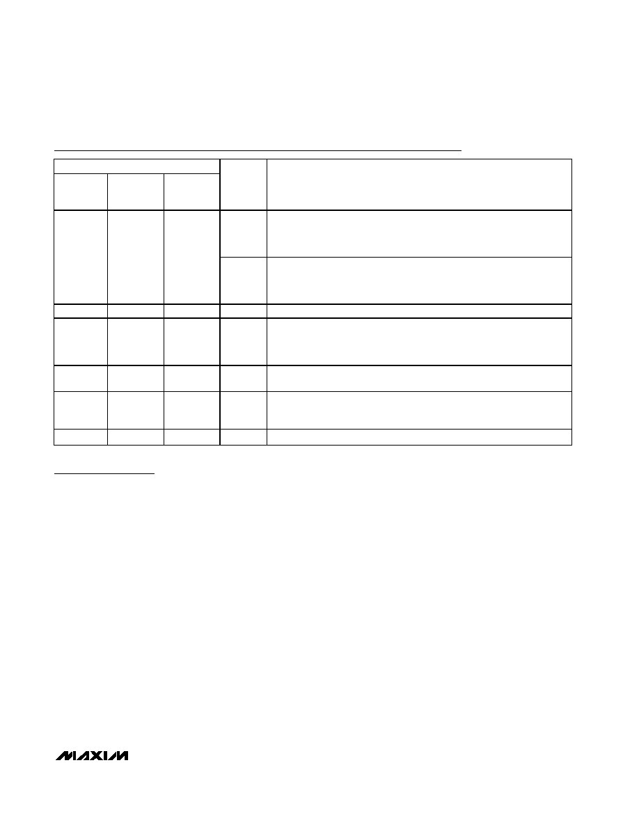
Pin Description
PIN
MAX6412/
MAX6413/
MAX6414
MAX6415/
MAX6416/
MAX6417
MAX6418/
MAX6419/
MAX6420
NAME
FUNCTION
RESET
RESET changes from high to low whenever V
CC
or RESET IN drops below
the selected reset threshold voltage (V
TH
or V
RESET IN
, respectively) or
manual reset is pulled low.
RESET remains low for the reset timeout period
after all reset conditions are deasserted and then goes high.
1
1
1
RESET
RESET changes from low to high whenever the V
CC
or RESET IN drops
below the selected reset threshold voltage (V
TH
or V
RESET IN
) or manual
reset is pulled low. RESET remains high for the reset timeout period after all
reset conditions are deasserted and then goes low.
2
2
2
GND
Ground
--
3
3
RESET
IN
Reset Input. High-impedance input to the adjustable reset comparator.
Connect RESET IN to the center point of an external resistor-divider
network to set the threshold of the externally monitored voltage. See Reset
Threshold section.
3
--
--
MR
Manual Reset Input. Pull this pin low to manually reset the device. Reset
remains asserted for the reset timeout period after
MR is released.
4
4
4
SRT
Set Reset Timeout Input. Connect a capacitor between SRT and ground to
set the timeout period. Determine the period as follows:
t
RP
= (2.73 x 10
6
)
C
SRT
+ 275Ás with t
RP
in seconds and C
SRT
in Farads.
5
5
5
V
CC
Supply Voltage and Input for Fixed-Threshold V
CC
Monitor