
General Description
The MAX6133 high-precision, low-power, low-dropout
voltage reference features a low 3ppm/░C (max) temper-
ature coefficient and a low dropout voltage (200mV,
max). This series-mode device features bandgap tech-
nology for low-noise performance and excellent accura-
cy. Load regulation specifications are guaranteed for
source currents up to 15mA. The laser-trimmed, high-
stability thin-film resistors, together with post-package
trimming, guarantee an excellent initial accuracy specifi-
cation (0.04%, max). The MAX6133 is a series voltage
reference and consumes only 40ÁA of supply current
(virtually independent of supply voltage). Series-mode
references save system power and use minimal external
components compared to 2-terminal shunt references.
The MAX6133 is available in 8-pin ÁMAX and SO pack-
ages. The unique blend of tiny packaging and excellent
precision performance make these parts ideally suited
for portable and communication applications.
Applications
Precision Regulators
A/D and D/A Converters
Power Supplies
High-Accuracy Industrial and Process Control
Hand-Held Instruments
Features
o Low Temperature Coefficient
3ppm/░C (max), SO
5ppm/░C (max), ÁMAX
o Tiny 5mm
3mm ÁMAX Package
o Low 200mV (max) Dropout Voltage
o Low 40ÁA Quiescent Current
o ▒0.04% (max) Initial Accuracy
o Low 16ÁV
P-P
Noise (0.1Hz to 10Hz) (2.5V Output)
o 15mA Output Source-Current Capability
o Wide 2.7V to 12.6V Supply Voltage
o Excellent Line (30ÁV/V, max) and
Load (0.05mV/mA, max) Regulation
MAX6133
3ppm/░C, Low-Power, Low-Dropout
Voltage Reference
________________________________________________________________ Maxim Integrated Products
1
OUT
I.C.*
GND
1
2
8
7
I.C.*
*INTERNALLY CONNECTED, DO NOT CONNECT.
N.C.
IN
N.C.
N.C.
SO/
ÁMAX
TOP VIEW
3
4
6
5
MAX6133
Pin Configuration
Ordering Information
MAX6133
OUT
SUPPLY INPUT
GND
*INPUT CAPACITORS ARE OPTIONAL.
IN
0.1
ÁF*
REFERENCE
OUTPUT
0.1
ÁF
Typical Operating Circuit
19-2266; Rev 2; 6/03
For pricing, delivery, and ordering information, please contact Maxim/Dallas Direct! at
1-888-629-4642, or visit Maxim's website at www.maxim-ic.com.
Note: Two-number part suffix indicates output voltage option.
PART
TEMP RANGE
PIN-PACKAGE
MAXIMUM INITIAL
ACCURACY (%)
MAXIMUM TEMPCO
(ppm/░C, -40
░C to +85░C)
MAX6133A_ _
-40░C to +125░C
8 ÁMAX
0.06
5
MAX6133AASA_ _
-40░C to +125░C
8 SO
0.04
3
MAX6133BASA_ _
-40░C to +125░C
8 SO
0.08
5
Selector Guide
SUFFIX
VOLTAGE OUTPUT
25
2.500V
30
3.000V
41
4.096V
50
5.000V

MAX6133
3ppm/░C, Low-Power, Low-Dropout
Voltage Reference
2
_______________________________________________________________________________________
ABSOLUTE MAXIMUM RATINGS
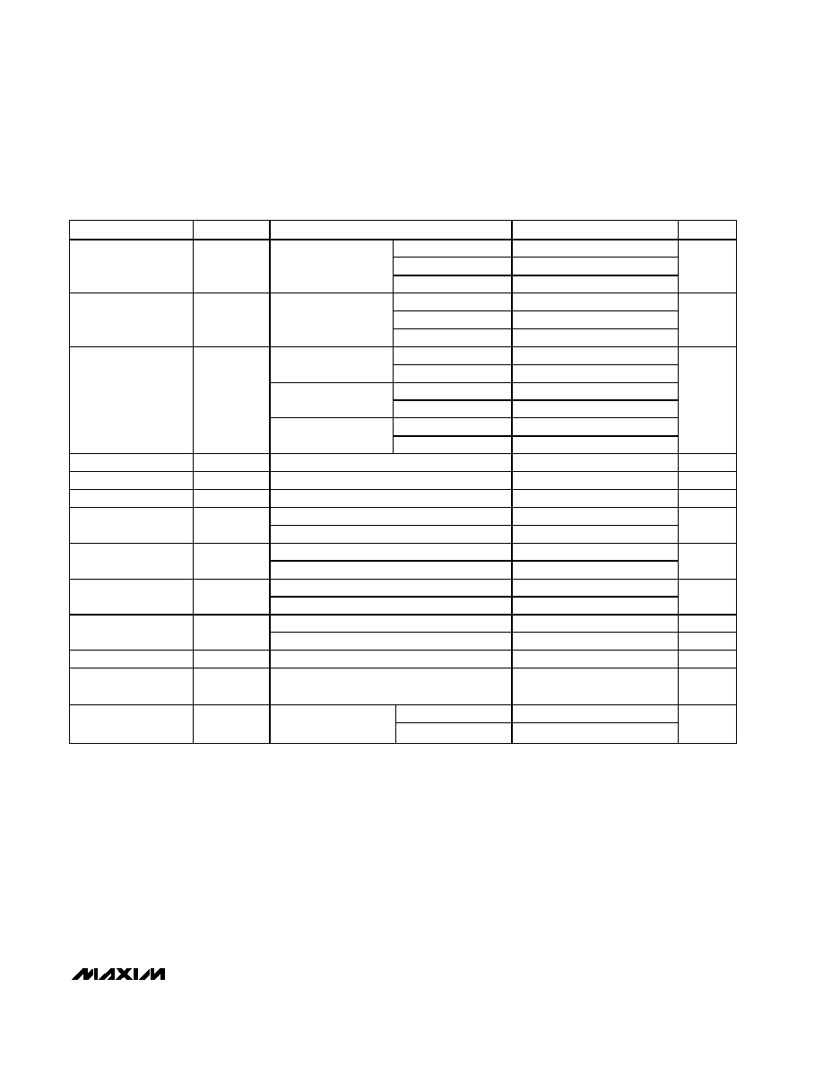
ELECTRICAL CHARACTERISTICS--MAX6133_25 (V
OUT
= 2.500V)
(V
IN
= 5V, C
LOAD
= 0.1ÁF, I
OUT
= 0, T
A
= T
MIN
to T
MAX
. Typical values are at T
A
= +25░C, unless otherwise noted.)
Stresses beyond those listed under "Absolute Maximum Ratings" may cause permanent damage to the device. These are stress ratings only, and functional
operation of the device at these or any other conditions beyond those indicated in the operational sections of the specifications is not implied. Exposure to
absolute maximum rating conditions for extended periods may affect device reliability.
Voltage (with Respect to GND)
IN ........................................................................-0.3V to +13V
OUT..............................................-0.3V to +6V or (V
IN
+ 0.3V)
OUT Short Circuit to IN or GND Duration ...............................60s
Continuous Power Dissipation (T
A
= +70░C)
8-Pin ÁMAX (derate 5.5mW/░C above +70░C) .............362mW
8-Pin SO (derate 5.88mW/░C above +70░C)................471mW
Operating Temperature Range .........................-40░C to +125░C
Storage Temperature Range .............................-65░C to +150░C
Junction Temperature ......................................................+150░C
Lead Temperature (soldering, 10s) .................................+300░C
PARAMETER
SYMBOL
CONDITIONS
MIN
TYP
MAX
UNITS
A grade SO
2.4990
2.5000
2.5010
B grade SO
2.4980
2.5000
2.5020
Output Voltage
V
OUT
T
A
= +25
░C
ÁMAX
2.4985
2.5000
2.5015
V
A grade SO
-0.04
+0.04
B grade SO
-0.08
+0.08
Output Voltage
Accuracy
T
A
= +25
░C
ÁMAX
-0.06
+0.06
%
T
A
= -40░C to +85
░C
1
3
A grade SO
T
A
= -40░C to +125
░C
4
7
T
A
= -40░C to +85
░C
3
5
B grade SO
T
A
= -40░C to +125
░C
5
10
T
A
= -40░C to +85
░C
1
5
Output Voltage
Temperature
Coefficient (Note 1)
TCV
OUT
ÁMAX
T
A
= -40░C to +125
░C
2
7
ppm/░C
Input Voltage Range
V
IN
Inferred from line regulation
2.7
12.6
V
Line Regulation
V
OUT
/
V
IN
2.7V
V
IN
12.6V
2
30
ÁV/V
Load Regulation
V
OUT
/
I
OUT
-100ÁA
I
OUT
15mA
0.003
0.05
mV/mA
V
OUT
= 0.1%, I
OUT
= 1mA
0.02
0.2
Dropout Voltage
(Note 2)
V
DO
V
OUT
= 0.1%, I
OUT
= 10mA
0.2
0.4
V
T
A
= +25
░C
40
60
Quiescent Supply
Current
I
IN
T
A
= -40
░C to +125░C
85
ÁA
Short to GND: V
OUT
= 0V
90
Output Short-Circuit
Current
I
SC
Short to V
IN
: V
OUT
= V
IN
-2
mA
0.1Hz
f 10Hz
16
ÁV
P-P
Output Voltage Noise
e
n
10Hz
f 1kHz
12
ÁV
RMS
Turn-On Settling Time
t
ON
V
OUT
settles to ▒0.01% of final value
500
Ás
Thermal Hysteresis
(Note 3)
120
ppm
SO
40
Long-Term Stability
t = 1000 hours
ÁMAX
145
ppm

MAX6133
3ppm/░C, Low-Power, Low-Dropout
Voltage Reference
_______________________________________________________________________________________
3
ELECTRICAL CHARACTERISTICS--MAX6133_30 (V
OUT
= 3.0000V)
(V
IN
= 5V, C
LOAD
= 0.1ÁF, I
OUT
= 0, T
A
= T
MIN
to T
MAX
. Typical values are at T
A
= +25░C, unless otherwise noted.)
PARAMETER
SYMBOL
CONDITIONS
MIN
TYP
MAX
UNITS
A grade SO
2.9988
3.0000
3.0012
B grade SO
2.9976
3.0000
3.0024
Output Voltage
V
OUT
T
A
= +25
░C
ÁMAX
2.9982
3.0000
3.0018
V
A grade SO
-0.04
+0.04
B grade SO
-0.08
+0.08
Output Voltage
Accuracy
T
A
= +25
░C
ÁMAX
-0.06
+0.06
%
T
A
= -40░C to +85
░C
1
3
A grade SO
T
A
= -40░C to +125
░C
4
7
T
A
= -40░C to +85
░C
3
5
B grade SO
T
A
= -40░C to +125
░C
5
10
T
A
= -40░C to +85
░C
1
5
Output Voltage
Temperature
Coefficient (Note 1)
TCV
OUT
ÁMAX
T
A
= -40░C to +125
░C
2
7
ppm/░C
Input Voltage Range
V
IN
Inferred from line regulation
3.2
12.6
V
Line Regulation
V
OUT
/
V
IN
3.2V
V
IN
12.6V
2
30
ÁV/V
Load Regulation
V
OUT
/
I
OUT
-100ÁA
I
OUT
15mA
0.003
0.06
mV/mA
V
OUT
= 0.1%, I
OUT
= 1mA
0.01
0.2
Dropout Voltage
(Note 2)
V
DO
V
OUT
= 0.1%, I
OUT
= 10mA
0.2
0.4
V
T
A
= +25
░C
40
60
Quiescent Supply
Current
I
IN
T
A
= -40
░C to +125░C
85
ÁA
Short to GND: V
OUT
= 0V
90
Output Short-Circuit
Current
I
SC
Short to V
IN
: V
OUT
= V
IN
-2
mA
0.1Hz
f 10Hz
24
ÁV
P-P
Output Voltage Noise
e
n
10Hz
f 1kHz
15
ÁV
RMS
Turn-On Settling Time
t
ON
V
OUT
settles to
▒0.01% of final value
600
Ás
Thermal Hysteresis
(Note 3)
120
ppm
SO
40
Long-Term Stability
t = 1000 hours
ÁMAX
145
ppm

MAX6133
3ppm/░C, Low-Power, Low-Dropout
Voltage Reference
4
_______________________________________________________________________________________
ELECTRICAL CHARACTERISTICS--MAX6133_41 (V
OUT
= 4.096V)
(V
IN
= 5V, C
LOAD
= 0.1ÁF, I
OUT
= 0, T
A
= T
MIN
to T
MAX
. Typical values are at T
A
= +25░C, unless otherwise noted.)
PARAMETER
SYMBOL
CONDITIONS
MIN
TYP
MAX
UNITS
A grade SO
4.0943
4.0960
4.0977
B grade SO
4.0927
4.0960
4.0993
Output Voltage
V
OUT
T
A
= +25
░C
ÁMAX
4.0935
4.0960
4.0985
V
A grade SO
-0.04
+0.04
B grade SO
-0.08
+0.08
Output Voltage
Accuracy
T
A
= +25
░C
ÁMAX
-0.06
+0.06
%
T
A
= -40░C to +85
░C
1
3
A grade SO
T
A
= -40░C to +125
░C
4
7
T
A
= -40░C to +85
░C
3
5
B grade SO
T
A
= -40░C to +125
░C
5
10
T
A
= -40░C to +85
░C
1
5
Output Voltage
Temperature
Coefficient (Note 1)
TCV
OUT
ÁMAX
T
A
= -40░C to +125
░C
2
7
ppm/░C
Input Voltage Range
V
IN
Inferred from line regulation
4.2
12.6
V
Line Regulation
V
OUT
/
V
IN
4.2V
V
IN
12.6V
2
40
ÁV/V
Load Regulation
V
OUT
/
I
OUT
-100ÁA
I
OUT
15mA
0.003
0.08
mV/mA
V
OUT
= 0.1%, I
OUT
= 1mA
0.01
0.2
Dropout Voltage
(Note 2)
V
DO
V
OUT
= 0.1%, I
OUT
= 10mA
0.2
0.4
V
T
A
= +25
░C
45
65
Quiescent Supply
Current
I
IN
T
A
= -40
░C to +125░C
85
ÁA
Short to GND: V
OUT
= 0V
90
Output Short-Circuit
Current
I
SC
Short to V
IN
: V
OUT
= V
IN
-2
mA
0.1Hz
f 10Hz
32
ÁV
P-P
Output Voltage Noise
e
n
10Hz
f 1kHz
22
ÁV
RMS
Turn-On Settling Time
t
ON
V
OUT
settles to ▒0.01% of final value
800
Ás
Thermal Hysteresis
(Note 3)
120
ppm
SO
40
Long-Term Stability
t = 1000 hours
ÁMAX
145
ppm
MAX6133
3ppm/░C, Low-Power, Low-Dropout
Voltage Reference
_______________________________________________________________________________________
5
ELECTRICAL CHARACTERISTICS--MAX6133_50 (V
OUT
= 5.000V)
(V
IN
= 5.5V, C
LOAD
= 0.1ÁF, I
OUT
= 0, T
A
= T
MIN
to T
MAX
. Typical values are at T
A
= +25░C, unless otherwise noted.)
PARAMETER
SYMBOL
CONDITIONS
MIN
TYP
MAX
UNITS
A grade SO
4.9980
5.0000
5.0020
B grade SO
4.9960
5.0000
5.0040
Output Voltage
V
OUT
T
A
= +25
░C
ÁMAX
4.9970
5.0000
5.0030
V
A grade SO
-0.04
+0.04
B grade SO
-0.08
+0.08
Output Voltage
Accuracy
T
A
= +25
░C
ÁMAX
-0.06
+0.06
%
T
A
= -40░C to +85
░C
1
3
A grade SO
T
A
= -40░C to +125
░C
4
7
T
A
= -40░C to +85
░C
3
5
B grade SO
T
A
= -40░C to +125
░C
5
10
T
A
= -40░C to +85
░C
1
5
Output Voltage
Temperature
Coefficient (Note 1)
TCV
OUT
ÁMAX
T
A
= -40░C to +125
░C
2
7
ppm/░C
Input Voltage Range
V
IN
Inferred from line regulation
5.2
12.6
V
Line Regulation
V
OUT
/
V
IN
5.2V
V
IN
12.6V
2
50
ÁV/V
Load Regulation
V
OUT
/
I
OUT
-100ÁA
I
OUT
15mA
0.01
0.10
mV/mA
V
OUT
= 0.1%, I
OUT
= 1mA
0.02
0.2
Dropout Voltage
(Note 2)
V
DO
V
OUT
= 0.1%, I
OUT
= 10mA
0.2
0.4
V
T
A
= +25
░C
40
60
Quiescent Supply
Current
I
IN
T
A
= -40
░C to +125░C
85
ÁA
Short to GND: V
OUT
= 0V
90
Output Short-Circuit
Current
I
SC
Short to V
IN
: V
OUT
= V
IN
-2
mA
0.1Hz
f 10Hz
40
ÁV
P-P
Output Voltage Noise
e
n
10Hz
f 1kHz
26
ÁV
RMS
Turn-On Settling Time
t
ON
V
OUT
settles to
▒0.01% of final value
1000
Ás
Thermal Hysteresis
(Note 3)
120
ppm
SO
40
Long-Term Stability
t = 1000 hours
ÁMAX
145
ppm
Note 1: The MAX6133 is 100% drift-tested for T
A
= T
MIN
to T
MAX
, as specified.
Note 2: Dropout Voltage is the minimum voltage at which V
OUT
changes
0.1% from V
OUT
at V
IN
= 5V (V
IN
= 5.5V for V
OUT
= 5V).
Note 3: Thermal Hysteresis is defined as the change in the initial +25
░C output voltage after cycling the device from T
MAX
to T
MIN
.