_______________General Description
The MAX603/MAX604 low-dropout, low quiescent cur-
rent, linear regulators supply 5V, 3.3V, or an adjustable
output for currents up to 500mA. They are available in a
1.8W SO package. Typical dropouts are 320mV at 5V
and 500mA, or 240mV at 3.3V and 200mA. Quiescent
currents are 15ÁA typ and 35ÁA max. Shutdown turns
off all circuitry and puts the regulator in a 2ÁA off mode.
A unique protection scheme limits reverse currents
when the input voltage falls below the output. Other fea-
tures include foldback current limiting and thermal
overload protection.
The output is preset at 3.3V for the MAX604 and 5V for
the MAX603. In addition, both devices employ Dual
ModeTM operation, allowing user-adjustable outputs
from 1.25V to 11V using external resistors. The input
voltage supply range is 2.7V to 11.5V.
The MAX603/MAX604 feature a 500mA P-channel
MOSFET pass transistor. This transistor allows the
devices to draw less than 35ÁA over temperature, inde-
pendent of the output current. The supply current
remains low because the P-channel MOSFET pass tran-
sistor draws no base currents (unlike the PNP transis-
tors of conventional bipolar linear regulators). Also,
when the input-to-output voltage differential becomes
small, the internal P-channel MOSFET does not suffer
from excessive base current losses that occur with sat-
urated PNP transistors.
________________________Applications
5V and 3.3V Regulators
1.25V to 11V Adjustable Regulators
Battery-Powered Devices
Pagers and Cellular Phones
Portable Instruments
Solar-Powered Instruments
____________________________Features
o
500mA Output Current, with Foldback Current
Limiting
o
High-Power (1.8W) 8-Pin SO Package
o
Dual ModeTM Operation: Fixed or Adjustable
Output from 1.25V to 11V
o
Large Input Range (2.7V to 11.5V)
o
Internal 500mA P-Channel Pass Transistor
o
15ÁA Typical Quiescent Current
o
2ÁA (Max) Shutdown Mode
o
Thermal Overload Protection
o
Reverse-Current Protection
______________Ordering Information
* Dice are tested at T
A
= +25░C, DC parameters only.
** Contact factory for availability.
MAX603/MAX604
5V/3.3V or Adjustable, Low-Dropout,
Low I
Q
, 500mA Linear Regulators
________________________________________________________________
Maxim Integrated Products
1
1
2
3
4
8
7
6
5
OUT
GND
GND
SET
IN
GND
GND
OFF
MAX603
MAX604
DIP/SO
TOP VIEW
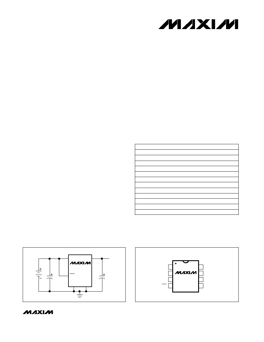
__________________Pin Configuration
MAX603
MAX604
OUT
SET
GND
IN
OFF
C
OUT
10
Á
F
C
IN
10
Á
F
BATTERY
OUTPUT
VOLTAGE
__________Typical Operating Circuit
Call toll free 1-800-998-8800 for free samples or literature.
19-0269; Rev 0; 9/94
PART
MAX603
CPA
MAX603CSA
MAX603C/D
0░C to +70░C
0░C to +70░C
0░C to +70░C
TEMP. RANGE
PIN-PACKAGE
8 Plastic DIP
8 SO
Dice*
MAX603EPA
MAX603ESA
-40░C to +85░C
-40░C to +85░C
8 Plastic DIP
8 SO
MAX603MJA
-55░C to +125░C
8 CERDIP**
MAX604
CPA
MAX604CSA
MAX604C/D
0░C to +70░C
0░C to +70░C
0░C to +70░C
8 Plastic DIP
8 SO
Dice*
MAX604EPA
MAX604ESA
-40░C to +85░C
-40░C to +85░C
8 Plastic DIP
8 SO
MAX604MJA
-55░C to +125░C
8 CERDIP**
TM Dual Mode is a trademark of Maxim Integrated Products.
MAX603/MAX604
5V/3.3V or Adjustable, Low-Dropout,
Low I
Q
, 500mA Linear Regulators
2
_______________________________________________________________________________________
ABSOLUTE MAXIMUM RATINGS
ELECTRICAL CHARACTERISTICS
(V
IN
= 6V (MAX603) or 4.3V (MAX604), C
IN
= C
OUT
= 10ÁF, OFF = V
IN
, SET = GND, T
J
= T
MIN
to T
MAX
, unless otherwise noted.
Typical values are at T
J
= +25░C.) (Note 1)
Stresses beyond those listed under "Absolute Maximum Ratings" may cause permanent damage to the device. These are stress ratings only, and functional
operation of the device at these or any other conditions beyond those indicated in the operational sections of the specifications is not implied. Exposure to
absolute maximum rating conditions for extended periods may affect device reliability.
Supply Voltage (IN or OUT to GND).......................-0.3V to +12V
Output Short-Circuit Duration ..............................................1 min
Continuous Output Current ...............................................600mA
SET, OFF Input Voltages ...........................-0.3V to the greater of
(IN + 0.3V) or (OUT + 0.3V)
Continuous Power Dissipation (T
A
= +70░C)
Plastic DIP (derate 9.09mW/░C above +70░C) ............727mW
SO (derate 23.6mW/░C above +70░C) .............................1.8W
CERDIP (derate 8.00mW/░C above +70░C) .................640mW
Operating Temperature Ranges
MAX60_C_A ........................................................0░C to +70░C
MAX60_E_A .....................................................-40░C to +85░C
MAX60_MJA ..................................................-55░C to +125░C
Junction Temperature ......................................................+150░C
Storage Temperature Range .............................-65░C to +160░C
Lead Temperature (soldering, 10sec) .............................+300░C
SET = OUT, R
L
= 1k
V
IN
= 11.5V, SET = OUT
OFF
0.4V, R
L
= 1k
,
(V
OUT
+ 1V)
V
IN
11.5V
I
OUT
= 500mA
I
OUT
= 200mA
3.0V
V
IN
11.5V, SET = OUT
I
OUT
= 1mA to 300mA
I
OUT
= 20ÁA to 500mA,
6.0V < V
IN
< 11.5V
I
OUT
= 20ÁA to 300mA,
4.3V < V
IN
< 11.5V
I
OUT
= 400mA
I
OUT
= 1mA to 500mA
I
OUT
= 200mA
mA
1200
I
LIM
Foldback Current Limit
(Note 4)
350
ÁA
20
I
OUT MIN
Minimum Load Current
6
2
ÁA
20
I
Q OFF
OFF Quiescent Current
10
0.01
2
ÁA
40
I
Q
Quiescent Current
15
35
mV
480
820
V
DO
Dropout Voltage (Note 3)
240
410
V
3.0
11.5
V
IN
Input Voltage
2.9
11.5
2.7
11.5
320
550
130
220
mV
7
40
V
LNR
Line Regulation
mV
30
100
V
LDR
Load Regulation
4.75
5.00
5.25
V
3.15
3.30
3.45
V
OUT
Output Voltage (Note 2)
60
100
150
UNITS
MIN
TYP
MAX
SYMBOL
PARAMETER
V
OUT
> 0.8V and V
IN
- V
OUT
> 0.7V
V
OUT
< 0.8V
MAX60_M
MAX60_M
MAX60_E
MAX60_E
MAX60_C
MAX60_C
MAX60_M
MAX60_E
MAX60_C
MAX603
MAX60_M
MAX60_C/E
(V
OUT
+ 0.5V)
V
IN
11.5V, I
OUT
= 25mA
MAX604
MAX603
MAX604
MAX603C/E
MAX604
MAX603M
CONDITIONS
░C
10
160
░C
Thermal Shutdown Hysteresis
T
SD
Thermal Shutdown Temperature
T
SD

Note 1:
Electrical specifications are measured by pulse testing and are guaranteed for a junction temperature (T
J
) equal to the
operating temperature range. C and E grade parts may be operated up to a T
J
of +125░. Expect performance similar to
M grade specifications. For T
J
between +125░C and +150░C, the output voltage may drift more.
Note 2:
(V
IN
- V
OUT
) is limited to keep the product (I
OUT
x (V
IN
- V
OUT
)) from exceeding the package power dissipation limits.
Note 3:
Dropout Voltage is (V
IN
- V
OUT
) when V
OUT
falls to 100mV below its nominal value at V
IN
= V
OUT
+ 2V. For example, the
MAX603 is tested by measuring the V
OUT
at V
IN
= 7V, then V
IN
is lowered until V
OUT
falls 100mV below the measured value.
The difference (V
IN
- V
OUT
) is then measured and defined as
V
DO
.
Note 4:
Foldback Current Limit was characterized by pulse testing to remain below the maximum junction temperature.
Note 5:
The Reverse-Current Protection Threshold is the output/input differential voltage (V
OUT
- V
IN
) at which reverse-current
protection switchover occurs and the pass transistor is turned off.
Note 6:
Noise is tested using a bandpass amplifier with two poles at 10Hz and two poles at 10kHz.
MAX603/MAX604
5V/3.3V or Adjustable, Low-Dropout,
Low I
Q
, 500mA Linear Regulators
_______________________________________________________________________________________
3
V
OUT
= 3.0V
V
OUT
= 4.5V
V
IN
= 11.5V, V
OUT
= 2V,
SET = OUT
V
IN
= 0V, V
OUT
= 4.5V (MAX603)
V
OUT
= 3.0V (MAX604)
ÁV
RMS
250
e
n
Output Noise (Note 6)
nA
▒0.01
▒10
I
OFF
OFF Input Leakage Current
4.0
V
IH OFF
OFF Threshold Voltage
3.0
2.0
V
0.4
20
I
OUT LKG
OUT Leakage Current
6
ÁA
0.01
2
nA
▒0.01
▒10
I
SET
SET Input Leakage Current
V
1.16
1.20
1.24
V
SET
SET Reference Voltage
150
80
V
SET TH
Dual-Mode SET Threshold
ÁA
0.01
10
6
20
V
RTH
mV
6
20
Reverse-Current Protection
Threshold (Note 5)
mV
80
30
t
START
%V
OUT
2
V
OSH
Start-Up Overshoot
20
100
UNITS
MIN
TYP
MAX
SYMBOL
PARAMETER
10Hz to 10kHz, SET = OUT, R
L
= 1k
,
C
OUT
= 10ÁF
V
OFF
= V
IN
or GND
MAX60_C
On, SET = OUT, V
IN
= 11.5V
On, SET = OUT, V
IN
= 6V
MAX604
On, SET = OUT, V
IN
= 4V
MAX603
Off
MAX60_M
MAX60_E
For internal feedback
V
IN
= 9V, R
L
= 18
, V
OFF
switched from
0V to V
IN
, time from 0% to 95% of V
OUT
MAX60_C
V
SET
= 1.5V or 0V
R
L
= 1k
, C
OUT
= 10ÁF, OFF rise time
1Ás
MAX60_E
MAX60_M
SET = OUT, R
L
= 1k
For external feedback
CONDITIONS
ELECTRICAL CHARACTERISTICS (continued)
(V
IN
= 6V (MAX603) or 4.3V (MAX604), C
IN
= C
OUT
= 10ÁF, OFF = V
IN
, SET = GND, T
J
= T
MIN
to T
MAX
, unless otherwise noted.
Typical values are at T
J
= +25░C.) (Note 1)
V
IL OFF
Reverse Leakage Current
I
RVL
Ás
200
Time Required to Exit Shutdown

MAX603/MAX604
5V/3.3V or Adjustable, Low-Dropout,
Low I
Q
, 500mA Linear Regulators
4
_______________________________________________________________________________________
__________________________________________Typical Operating Characteristics
(V
IN
= 7V for MAX603, V
IN
= 5.3V for MAX604, OFF = V
IN
, SET = GND, C
IN
= C
OUT
= 10ÁF, R
L
= 1k
, T
J
= +25░C, unless otherwise noted.)
1.00
1.01
0.95
0.1
10
700
OUTPUT VOLTAGE vs. LOAD CURRENT
0.96
MAX603/4-TOC-01
LOAD CURRENT (mA)
NORMALIZED OUTPUT VOLTAGE
0.97
0.98
0.99
1
100
V
OUT
= 3.3V, 5V, 10V
NORMALIZED TO
OUTPUT VOLTAGE
AT 1mA
25
30
0
0.1
10
700
QUIESCENT CURRENT vs. LOAD CURRENT
5
MAX603/4-TOC-02
LOAD CURRENT (mA)
QUIESCENT CURRENT (
Á
A)
10
15
20
1
100
UPWARD CURVE IS
THERMAL EFFECT
MAX603, V
IN
= 12V, V
OUT
= 10V
MAX603, V
IN
= 7V, V
OUT
= 5V
MAX604, V
IN
= 5.3V, V
OUT
= 3.3V
0
2
OUTPUT VOLTAGE AND
QUIESCENT CURRENT vs. SUPPLY VOLTAGE
MAX1603/4 TOC-03
SUPPLY VOLTAGE (V)
OUTPUT VOLTAGE (V)
QUIESCENT CURRENT (
Á
A)
8
4
2
4
6
12
6
3
1
5
10
3
9
5
7
11
24
22
20
18
16
14
12
10
8
6
MAX603, V
OUT
= 5V
MAX604, V
OUT
= 3.3V
I
Q
, MAX604
I
Q
, MAX603
96
97
98
99
100
101
102
103
104
-55
45
125
OUTPUT VOLTAGE vs.
TEMPERATURE
MAX603/4-TOC-04
TEMPERATURE (░C)
NORMALIZED OUTPUT VOLTAGE (%)
5
-35
85
65
25
-15
105
10ms/div
10Hz TO 10kHz OUTPUT NOISE
OUTPUT NOISE (1mV/div)
MAX603
V
OUT
= 5V
0
5
10
15
20
25
-55
45
125
QUIESCENT CURRENT vs.
TEMPERATURE
MAX603/4-TOC-05
TEMPERATURE (░C)
QUIESCENT CURRENT (
Á
A)
5
-35
85
65
25
-15
105
MAX603
MAX604
0
0.1
0.2
0.3
0.4
0.5
0.6
0.7
0.8
0.9
0
500
DROPOUT VOLTAGE vs. LOAD CURRENT
MAX603/4-TOC-06
LOAD CURRENT (mA)
DROPOUT VOLTAGE (V)
300
100
700
600
400
200
MAX604
V
OUT
= 3.3V
MAX603
V
OUT
= 5V
MAX603, V
OUT
= 10V,
SET EXTERNALLY
R
DS(ON)
= 0.4
R
DS(ON)
= 0.65
R
DS(ON)
= 1.2
2ms/div
LINE-TRANSIENT RESPONSE
A: V
IN
= 8V (HIGH), V
IN
= 7V (LOW)
B: OUTPUT VOLTAGE (50mV/div)
A
B
MAX603
V
OUT
= 5V
t
R
= 10
Á
s, t
F
= 70
Á
s

MAX603/MAX604
5V/3.3V or Adjustable, Low-Dropout,
Low I
Q
, 500mA Linear Regulators
_______________________________________________________________________________________
5
2ms/div
LOAD-TRANSIENT RESPONSE
A: OUTPUT VOLTAGE (100mV/div)
B: I
OUT
= 500mA (HIGH), I
OUT
= 5mA (LOW)
A
B
MAX603
V
OUT
= 5V
_____________________________Typical Operating Characteristics (continued)
(V
IN
= 7V for MAX603, V
IN
= 5.3V for MAX604, OFF = V
IN
, SET = GND, C
IN
= C
OUT
= 10ÁF, R
L
= 1k
, T
J
= +25░C, unless otherwise noted.)
500
Á
s/div
OVERSHOOT AND TIME
EXITING SHUTDOWN MODE
A: OFF PIN VOLTAGE (1V/div)
RISE TIME = 13
Á
s
B: MAX603 OUTPUT VOLTAGE (1V/div)
DELAY = 4.936ms, OVERSHOOT = 1%, RISE TIME = 55
Á
s
A
0V
5V
B
______________________________________________________________Pin Description
PIN
NAME
DESCRIPTION
1
IN
Regulator Input. Supply voltage can range from 2.7V to 11.5V.
2, 3, 6, 7
GND
Ground. These pins function as heatsinks, only in the SOIC package. All GND pins must be soldered to the
circuit board for proper power dissipation. Connect to large copper pads or planes to channel heat from the IC.
4
OFF
Shutdown, active low. Switch logic levels in less than 1Ás with the high level above the OFF threshold.
5
SET
Feedback for Setting the Output Voltage. Connect to GND to set the output voltage to the preselected 3.3V
or 5V. Connect to an external resistor network for adjustable output operation.
8
OUT
Regulator Output. Fixed or adjustable from 1.25V to 11.0V. Sources up to 500mA for input voltages above 4V.
MAX603
MAX604
OUT
GND
GND
SET
IN
OFF
C
OUT
10
Á
F
C
IN
10
Á
F
V
IN
V
OUT
GND
GND
R1
R2
R
L
1
2
3
4
8
7
6
5
Figure 1. Test Circuit