General Description
The MAX5888 is an advanced, 16-bit, 500Msps digital-
to-analog converter (DAC) designed to meet the
demanding performance requirements of signal synthe-
sis applications found in wireless base stations and
other communications applications. Operating from a
single 3.3V supply, this DAC offers exceptional dyna-
mic performance such as 76dBc spurious-free dynamic
range (SFDR) at f
OUT
= 40MHz. The DAC supports
update rates of 500Msps and a power dissipation of
only 250mW.
The MAX5888 utilizes a current-steering architecture,
which supports a full-scale output current range of 2mA
to 20mA, and allows a differential output voltage swing
between 0.1V
P-P
and 1V
P-P
.
The MAX5888 features an integrated 1.2V bandgap ref-
erence and control amplifier to ensure high accuracy
and low noise performance. Additionally, a separate
reference input pin enables the user to apply an exter-
nal reference source for optimum flexibility and to
improve gain accuracy.
The digital and clock inputs of the MAX5888 are
designed for differential low-voltage differential signal
(LVDS)-compatible voltage levels. The MAX5888 is
available in a 68-lead QFN package with an exposed
paddle (EP) and is specified for the extended industrial
temperature range (-40°C to +85°C).
Refer to the MAX5887 and MAX5886 data sheets for
pin-compatible 14- and 12-bit versions of the MAX5888.
Applications
Base Stations: Single-/Multicarrier UMTS,
CDMA, GSM
Communications: LMDS, MMDS, Point-to-Point
Microwave
Digital Signal Synthesis
Automated Test Equipment (ATE)
Instrumentation
Features
o 500Msps Output Update Rate
o Single 3.3V Supply Operation
o Excellent SFDR and IMD Performance
SFDR = 76dBc at f
OUT
= 40MHz (to Nyquist)
IMD = -85dBc at f
OUT
= 10MHz
ACLR = 73dB at f
OUT
= 61MHz
o 2mA to 20mA Full-Scale Output Current
o Differential, LVDS-Compatible Digital and Clock
Inputs
o On-Chip 1.2V Bandgap Reference
o Low 130mW Power Dissipation
o 68-Lead QFN-EP Package
MAX5888
3.3V, 16-Bit, 500Msps High Dynamic
Performance DAC with Differential LVDS Inputs
________________________________________________________________ Maxim Integrated Products
1
Ordering Information
19-2726; Rev 3; 12/03
For pricing, delivery, and ordering information, please contact Maxim/Dallas Direct! at
1-888-629-4642, or visit Maxim's website at www.maxim-ic.com.
PART
TEMP RANGE
PIN-
PACKAGE
MAX5888AEGK
-40
°C to +85°C
68 QFN-EP*
MAX5888EGK
-40
°C to +85°C
68 QFN-EP*
58
59
60
61
62
54
55
56
57
63
38
39
40
41
42
43
44
45
46
47
VCLK
AGND
B6P
QFN
TOP VIEW
DGND
DV
DD
DGND
B7N
B7P
B8N
B8P
B9N
B9P
52
53
B10N
B10P
AV
DD
FSADJ
REFIO
N.C.
DACREF
AGND
AV
DD
IOUTP
IOUTN
AV
DD
AGND
AGND
AV
DD
AV
DD
B13N
B13P
B14N
B14P
B15N
B15P
DGND
DV
DD
SEL0
N.C.
35
36
37
N.C.
N.C.
N.C.
DV
DD
DGND
B0N
B0P
B1N
VCLK
CLKGND
CLKN
CLKP
CLKGND
B1P
B2N
B2P
B3N
48
B12P
B3P
64
B6N
65
66
67
B4P
B5N
B5P
68
B4N
23
22
21
20
19
27
26
25
24
18
29
28
32
31
30
AGND
N.C.
34
33
49
50
B11P
B12N
51
B11N
11
10
9
8
7
6
5
4
3
2
16
15
14
13
12
1
PD
17
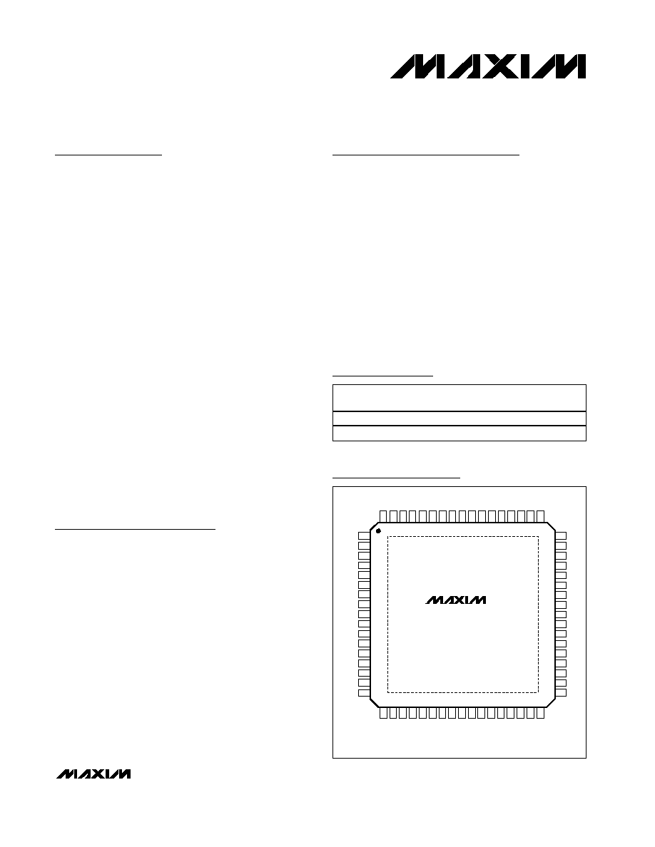
MAX5888
EP
Pin Configuration
*EP = Exposed paddle.
MAX5888
3.3V, 16-Bit, 500Msps High Dynamic
Performance DAC with Differential LVDS Inputs
2
_______________________________________________________________________________________
ABSOLUTE MAXIMUM RATINGS
ELECTRICAL CHARACTERISTICS
(AV
DD
= DV
DD
= VCLK = 3.3V, AGND = DGND = CLKGND = 0, external reference, V
REFIO
= 1.25V, differential transformer-coupled
analog output, 50
double terminated (Figure 7), I
OUT
= 20mA, T
A
= T
MIN
to T
MAX
, unless otherwise noted.
+25°C guaranteed by
production test, <+25°C guaranteed by design and characterization. Typical values are at T
A
= +25°C.)
Stresses beyond those listed under "Absolute Maximum Ratings" may cause permanent damage to the device. These are stress ratings only, and functional
operation of the device at these or any other conditions beyond those indicated in the operational sections of the specifications is not implied. Exposure to
absolute maximum rating conditions for extended periods may affect device reliability.
AV
DD
, DV
DD
, VCLK to AGND................................-0.3V to +3.9V
AV
DD
, DV
DD
, VCLK to DGND ...............................-0.3V to +3.9V
AV
DD
, DV
DD
, VCLK to CLKGND ...........................-0.3V to +3.9V
AGND, CLKGND to DGND....................................-0.3V to +0.3V
DACREF, REFIO, FSADJ to AGND.............-0.3V to AV
DD
+ 0.3V
IOUTP, IOUTN to AGND................................-1V to AV
DD
+ 0.3V
CLKP, CLKN to CLKGND...........................-0.3V to VCLK + 0.3V
B0P/B0NB15P/B15N, SEL0,
PD to DGND ...........................................-0.3V to DV
DD
+ 0.3V
Continuous Power Dissipation (T
A
= +70°C)
68-Lead QFN-EP (derate 41.7mW/°C above +70°C) ...3333mW
Thermal Resistance (
JA
) ..............................................+24°C/W
Operating Temperature Range ..........................-40°C to +85°C
Junction Temperature .....................................................+150°C
Storage Temperature Range ............................-60°C to +150°C
Lead Temperature (soldering, 10s) ................................+300°C
PARAMETER
SYMBOL
CONDITIONS
MIN
TYP
MAX
UNITS
STATIC PERFORMANCE
Resolution
16
Bits
MAX5888A___, measured differentially,
T
A
+25°C
-0.008
±0.004
+0.008
Integral Nonlinearity
INL
MAX5888___, measured differentially,
T
A
+25°C
±0.006
% FS
MAX5888A___, measured differentially,
T
A
+25°C
-0.006
±0.002
+0.006
Differential
Nonlinearity
DNL
MAX5888___, measured differentially,
T
A
+25°C
±0.003
% FS
Offset Error
OS
-0.025
±0.003 +0.025
%FS
Offset Drift
±50
ppm/
°C
Full-Scale Gain Error
GE
FS
External reference, T
A
+25°C
-3.1
+1.1
%FS
Internal reference
±100
Gain Drift
External reference
±50
ppm/
°C
Full-Scale Output Current
I
OUT
(Note 1)
2
20
mA
Min Output Voltage
Single ended
-0.5
V
Max Output Voltage
Single ended
1.1
V
Output Resistance
R
OUT
1
M
Output Capacitance
C
OUT
5
pF
DYNAMIC PERFORMANCE
Output Update Rate
f
CLK
1
500
Msps
f
CLK
= 300MHz
f
OUT
= 16MHz, -12dB FS
-165
Noise Spectral Density
f
CLK
= 500MHz
f
OUT
= 16MHz, -12dB FS
-164
dB FS/
Hz
f
OUT
= 1MHz, 0dB FS
88
f
OUT
= 1MHz, -6dB FS
89
Spurious-Free Dynamic Range to
Nyquist
SFDR
f
CLK
= 100MHz
f
OUT
= 1MHz, -12dB FS
85
dBc

MAX5888
3.3V, 16-Bit, 500Msps High Dynamic
Performance DAC with Differential LVDS Inputs
_______________________________________________________________________________________
3
ELECTRICAL CHARACTERISTICS (continued)
(AV
DD
= DV
DD
= VCLK = 3.3V, AGND = DGND = CLKGND = 0, external reference, V
REFIO
= 1.25V, differential transformer-coupled
analog output, 50
double terminated (Figure 7), I
OUT
= 20mA, T
A
= T
MIN
to T
MAX
, unless otherwise noted.
+25°C guaranteed by
production test, <+25°C guaranteed by design and characterization. Typical values are at T
A
= +25°C.)
PARAMETER
SYMBOL
CONDITIONS
MIN
TYP
MAX
UNITS
f
OUT
= 10MHz, -12dB FS
82
f
CLK
= 100MHz
f
OUT
= 30MHz, -12dB FS
79
f
OUT
= 10MHz, -12dB FS
73
f
OUT
= 16MHz, -12dB FS,
T
A
+25°C
69
77
f
OUT
= 50MHz, -12dB FS
72
f
CLK
= 200MHz
f
OUT
= 80MHz, -12dB FS
66
f
OUT
= 10MHz, -12dB FS
67
f
OUT
= 30MHz, -12dB FS
65
f
OUT
= 50MHz, -12dB FS
65
Spurious-Free Dynamic Range to
Nyquist
SFDR
f
CLK
= 500MHz
f
OUT
= 80MHz, -12dB FS
63
dBc
Spurious-Free Dynamic Range,
25MHz Bandwidth
SFDR
f
CLK
= 150MHz f
OUT
= 20MHz, -12dB FS
82
dBc
f
CLK
= 100MHz
f
OUT1
= 9MHz, -6dB FS,
f
OUT2
= 10MHz, -6dB FS
-85
2-Tone IMD
TTIMD
f
CLK
= 300MHz
f
OU T 1
= 49M H z, - 12d B FS ,
f
OU T 2
= 50M H z, - 12d B FS
-83
dBc
4-Tone IMD, 1MHz Frequency
Spacing, GSM Model
FTIMD
f
CLK
= 300MHz f
OUT
= 32MHz, -12dB FS
-78
dBc
Adjacent Channel Leakage
Power Ratio, 4.1MHz Bandwidth,
WCDMA Model
ACLR
f
CLK
=
184.32MHz
f
OUT
= 61.44MHz
73
dB
Output Bandwidth
BW
-1dB
(Note 2)
450
MHz
REFERENCE
Internal Reference Voltage Range
V
REFIO
1.13
1.22
1.3
V
Reference Voltage Drift
TCO
REF
±50
ppm/
°C
Reference Input Compliance
Range
V
REFIOCR
0.125
1.250
V
Reference Input Resistance
R
REFIO
10
k
ANALOG OUTPUT TIMING
Output Fall Time
t
FALL
90% to 10% (Note 3)
375
ps
Output Rise Time
t
RISE
10% to 90% (Note 3)
375
ps
Output Voltage Settling Time
t
SETTLE
Output settles to 0.025% FS (Note 3)
11
ns
Output Propagation Delay
t
PD
(Note 3)
1.8
ns
Glitch Energy
1
pV-s
I
OUT
= 2mA
30
Output Noise
N
OUT
I
OUT
= 20mA
30
pA/
Hz
MAX5888
3.3V, 16-Bit, 500Msps High Dynamic
Performance DAC with Differential LVDS Inputs
4
_______________________________________________________________________________________
ELECTRICAL CHARACTERISTICS (continued)
(AV
DD
= DV
DD
= VCLK = 3.3V, AGND = DGND = CLKGND = 0, external reference, V
REFIO
= 1.25V, differential transformer-coupled
analog output, 50
double terminated (Figure 7), I
OUT
= 20mA, T
A
= T
MIN
to T
MAX
, unless otherwise noted.
+25°C guaranteed by
production test, <+25°C guaranteed by design and characterization. Typical values are at T
A
= +25°C.)
PARAMETER
SYMBOL
CONDITIONS
MIN
TYP
MAX
UNITS
TIMING CHARACTERISTICS
Data to Clock Setup Time
t
SETUP
Referenced to rising edge of clock (Note 4)
-0.8
ns
Data to Clock Hold Time
t
HOLD
Referenced to rising edge of clock (Note 4)
1.8
ns
Data Latency
3.5
Clock
cycles
Minimum Clock Pulse Width High
t
CH
CLKP, CLKN
0.9
ns
Minimum Clock Pulse Width Low
t
CL
CLKP, CLKN
0.9
ns
LVDS LOGIC INPUTS (B0NB15N, B0PB15P)
Differential Input Logic High
V
IH
100
mV
Differential Input Logic Low
V
IL
-100
mV
Common-Mode Voltage Range
V
COM
1.125
1.375
V
Differential Input Resistance
R
IN
85
100
125
Input Capacitance
C
IN
5
pF
CMOS LOGIC INPUTS (PD, SEL0)
Input Logic High
V
IH
0.7
DV
DD
V
Input Logic Low
V
IL
0.3
DV
DD
V
Input Leakage Current
I
IN
-15
+15
µA
Input Capacitance
C
IN
5
pF
CLOCK INPUTS (CLKP, CLKN)
Sine wave
1.5
Differential Input Voltage Swing
V
CLK
Square wave
0.5
V
P-P
Differential Input Slew Rate
SR
CLK
(Note 5)
>100
V/µs
Common-Mode Voltage Range
V
COM
1.5
±20%
V
Input Resistance
R
CLK
5
k
Input Capacitance
C
CLK
5
pF
POWER SUPPLIES
Analog Supply Voltage Range
AV
DD
3.135
3.3
3.465
V
Digital Supply Voltage Range
DV
DD
3.135
3.3
3.465
V
Clock Supply Voltage Range
V
CLK
3.135
3.3
3.465
V
f
CLK
= 100Msps, f
OUT
= 1MHz
27
Analog Supply Current
I
AVDD
Power-down
0.3
mA
f
CLK
= 100Msps, f
OUT
= 1MHz
7
mA
Digital Supply Current
I
DVDD
Power-down
10
µA
f
CLK
= 100Msps, f
OUT
= 1MHz
5.6
mA
Clock Supply Current
I
VCLK
Power-down
10
µA

MAX5888
3.3V, 16-Bit, 500Msps High Dynamic
Performance DAC with Differential LVDS Inputs
_______________________________________________________________________________________
5
Note 1: Nominal full-scale current I
OUT
= 32
I
REF
.
Note 2: This parameter does not include update-rate depending effects of sin(x)/x filtering inherent in the MAX5888.
Note 3: Parameter measured single ended into a 50
termination resistor.
Note 4: Parameter guaranteed by design.
Note 5: A differential clock input slew rate of >100V/ms is required to achieve the specified dynamic performance.
Note 6: Parameter defined as the change in midscale output caused by a ±5% variation in the nominal supply voltage.
PARAMETER
SYMBOL
CONDITIONS
MIN
TYP
MAX
UNITS
f
CLK
= 100Msps, f
OUT
= 1MHz
130
Power Dissipation
P
DISS
Power-down
1
mW
Power-Supply Rejection Ratio
PSRR
AV
DD
= VCLK = DV
DD
= 3.3V
±5% (Note 6)
-1
+1
%FS/V
ELECTRICAL CHARACTERISTICS (continued)
(AV
DD
= DV
DD
= VCLK = 3.3V, AGND = DGND = CLKGND = 0, external reference, V
REFIO
= 1.25V, differential transformer-coupled
analog output, 50
double terminated (Figure 7), I
OUT
= 20mA, T
A
= T
MIN
to T
MAX
, unless otherwise noted.
+25°C guaranteed by
production test, <+25°C guaranteed by design and characterization. Typical values are at T
A
= +25°C.)
Typical Operating Characteristics
(AV
DD
= DV
DD
= VCLK = 3.3V, external reference, V
REFIO
= 1.25V, R
L
= 50
, I
OUT
= 20mA, T
A
= +25°C, unless otherwise noted.)
0
30
20
10
40
50
60
70
80
90
100
0
20
10
30
40
50
SPURIOUS-FREE DYNAMIC RANGE
vs. OUTPUT FREQUENCY (f
CLK
= 100MHz)
MAX5888 toc01
f
OUT
(MHz)
SFDR (dBc)
-12dB FS
0dB FS
-6dB FS
0
30
20
10
40
50
60
70
80
90
100
0
40
20 30
50
70
90
10
60
80
100
SPURIOUS-FREE DYNAMIC RANGE
vs. OUTPUT FREQUENCY (f
CLK
= 200MHz)
MAX5888 toc02
f
OUT
(MHz)
SFDR (dBc)
-6dB FS
-12dB FS
0dB FS
0
30
20
10
40
50
60
70
80
90
100
0
100
50
150
200
250
SPURIOUS-FREE DYNAMIC RANGE
vs. OUTPUT FREQUENCY (f
CLK
= 500MHz)
MAX5888 toc03
f
OUT
(MHz)
SFDR (dBc)
-6dB FS
0dB FS
-12dB FS
-100
-70
-80
-90
-60
-50
-40
-30
-20
-10
0
7
9
8
10
11
12
2-TONE INTERMODULATION DISTORTION
(f
CLK
= 100MHz)
MAX5888 toc04
f
OUT
(MHz)
2-TONE IMD (dBm)
2 x f
T1
- f
T2
2 x f
T2
- f
T1
f
T2
f
T1
A
OUT
= -6dB FS
BW = 5MHz
f
T1
= 9.0252MHz
f
T2
= 10.0417MHz
-40
-60
-50
-80
-70
-90
-100
0
2-TONE IMD vs. OUTPUT FREQUENCY
(1MHz CARRIER SPACING, f
CLK
= 300MHz)
MAX5888 toc05
f
OUT
(MHz)
TWO-TONE IMD (dBc)
50
25
75
100
-6dB FS
-12dB FS
-100
-70
-80
-90
-60
-50
-40
-30
-20
-10
0
77
79
78
80
81
82
2-TONE INTERMODULATION DISTORTION
(f
CLK
= 450MHz)
MAX5888 toc06
f
OUT
(MHz)
2-TONE IMD (dBm)
2 x f
T1
- f
T2
2 x f
T2
- f
T1
f
T2
f
T1
A
OUT
= -6dB FS
BW = 5MHz
f
T1
= 79.2114MHz
f
T2
= 80.0903MHz