MAX5527 DS
General Description
The MAX5527/MAX5528/MAX5529 linear-taper digital
potentiometers perform the same function as mechanical
potentiometers, replacing the mechanics with a simple
2-wire up/down digital interface. These digital poten-
tiometers provide an optional one-time programmable
feature that sets the power-on reset position of the wiper.
Once the wiper position is programmed, the 2-wire inter-
face can be disabled to prevent unwanted adjustment.
The MAX5527/MAX5528/MAX5529 provide an end-to-end
resistance of 100k
, 50k, and 10k, respectively. The
devices feature low temperature coefficients of 35ppm/
°C
end-to-end and 5ppm/
°C ratiometric. All devices offer 64
wiper positions and operate from a single +2.7V to +5.5V
supply. An ultra-low, 0.25µA (typ) standby supply current
saves power in battery-operated applications.
The MAX5527/MAX5528/MAX5529 are available in
3mm x 3mm, 8-pin TDFN and 5mm x 3mm, 8-pin
µMAX
®
packages. Each device is guaranteed over the
-40
°C to +105°C temperature range.
Applications
Products Using One-Time Factory Calibration
Mechanical Potentiometer Replacements
Features
o Wiper Position Stored After One-Time Fuse
Programming
o 64 Tap Positions
o Wiper Position Programmed Through Simple
2-Wire Up/Down Interface
o 35ppm/°C End-to-End Temperature Coefficient
o 5ppm/°C Ratiometric Temperature Coefficient
o Ultra-Low 1.5µA (max) Static Supply Current
o +2.7V to +5.5V Single-Supply Operation
o 10k, 50k, and 100k End-to-End Resistances
o Tiny, 3mm x 3mm, 8-Pin TDFN and 5mm x 3mm,
8-Pin µMAX Packages
MAX5527/MAX5528/MAX5529
One-Time Programmable, Linear-Taper Digital
Potentiometers
________________________________________________________________ Maxim Integrated Products
1
Ordering Information
19-3665; Rev 0; 5/05
For pricing, delivery, and ordering information, please contact Maxim/Dallas Direct! at
1-888-629-4642, or visit Maxim's website at www.maxim-ic.com.
PART
PIN-PACKAGE
RESISTANCE
(k
)
TOP
MARK
MAX5527GTA
8 TDFN-EP*
100
AOG
MAX5527GUA
8 µMAX
100
--
MAX5528GTA
8 TDFN-EP*
50
AOH
MAX5528GUA
8 µMAX
50
--
MAX5529GTA
8 TDFN-EP*
10
AOI
MAX5529GUA
8 µMAX
10
--
*EP = Exposed pad.
All devices operate over the -40°C to +105°C temperature range.
1
H
V
DD
CS
GND
µMAX
TDFN*
TOP VIEW
2
3
4
L
U/
D
PV
8
7
6
5
W
*EXPOSED PADDLE. CONNECT TO GND.
MAX5527
MAX5528
MAX5529
1
H
V
DD
CS
GND
2
3
4
L
U/
D
PV
8
7
6
5
W
MAX5527
MAX5528
MAX5529
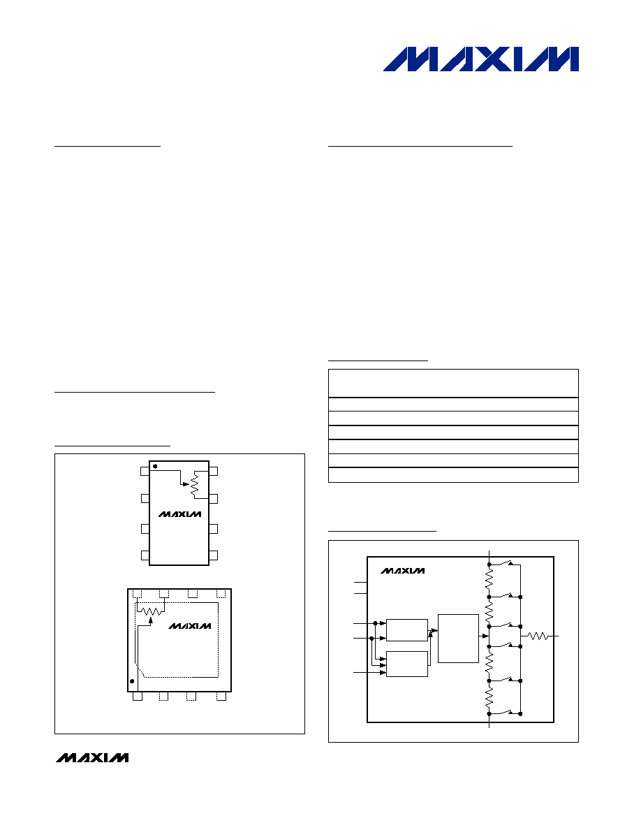
Pin Configurations
µMAX is a registered trademark of Maxim Integrated Products, Inc.
Functional Diagram
MAX5527
MAX5528
MAX5529
64-
POSITION
DECODER
UP/DOWN
COUNTER
ONE-TIME
PROGRAM
BLOCK
V
DD
GND
CS
U/
D
PV
L
H
W
R
62
R
61
R
1
R
0
S
63
S
62
S
61
S
2
S
1
S
0
R
W
MAX5527/MAX5528/MAX5529
One-Time Programmable, Linear-Taper Digital
Potentiometers
2
_______________________________________________________________________________________
ABSOLUTE MAXIMUM RATINGS
Stresses beyond those listed under "Absolute Maximum Ratings" may cause permanent damage to the device. These are stress ratings only, and functional
operation of the device at these or any other conditions beyond those indicated in the operational sections of the specifications is not implied. Exposure to
absolute maximum rating conditions for extended periods may affect device reliability.
V
DD
to GND ...........................................................-0.3V to +6.0V
PV to GND ...........................................................-0.3V to +12.0V
All Other Pins to GND.................................-0.3V to (V
DD
+ 0.3V)
Maximum Continuous Current into H, L, and W
MAX5527 ......................................................................±0.5mA
MAX5528 ......................................................................±1.0mA
MAX5529 ......................................................................±2.0mA
Continuous Power Dissipation (T
A
= +70°C)
8-Pin µMAX (derate 4.5mW/°C above +70°C) ..............362mW
8-Pin TDFN (derate 18.2mW/°C above +70°C) .......1454.5mW
Operating Temperature Range .........................-40°C to +105°C
Junction Temperature ......................................................+150°C
Storage Temperature Range .............................-65°C to +150°C
Lead Temperature (soldering, 10s) .................................+300°C
ELECTRICAL CHARACTERISTICS
(V
DD
= +2.7V to +5.5V, V
H
= V
DD
, V
L
= GND, T
A
= -40
°C to +105°C, unless otherwise noted. Typical values are at V
DD
= +5.0V, T
A
= +25
°C.) (Note 1)
PARAMETER
SYMBOL
CONDITIONS
MIN
TYP
MAX
UNITS
DC PERFORMANCE
Resolution
64
Taps
MAX5527
75
100
125
MAX5528
37.5
50
62.5
End-to-End Resistance
MAX5529
7.5
10
12.5
k
End-to-End Resistance
Temperature Coefficent
TC
R
35
ppm/
°C
MAX5527/MAX5528
5
Resistance Ratio Temperature
Coefficient
MAX5529
10
ppm/
°C
Integral Nonlinearity
INL
Potentiometer configuration, no load,
Figure 1
±0.025
±1
LSB
Differential Nonlinearity
DNL
Potentiometer configuration, no load,
Figure 1
±0.01
±1
LSB
Full-Scale Error
Potentiometer configuration, no load,
Figure 1
-0.005
-1
LSB
Zero-Scale Error
Potentiometer configuration, no load,
Figure 1
+0.006
+1
LSB
V
DD
3V
90
200
Wiper Resistance (Note 2)
R
W
V
DD
< 3V
125
650
DYNAMIC CHARACTERISTICS
MAX5527
100
MAX5528
200
Wiper -3dB Bandwidth (Note 3)
MAX5529
1000
kHz
MAX5527
-78
MAX5528
-82
Total Harmonic Distortion
f = 10kHz, midscale, 1V
RMS
R
L
= 100k
MAX5529
-94
dB
MAX5527/MAX5528/MAX5529
One-Time Programmable, Linear-Taper Digital
Potentiometers
_______________________________________________________________________________________
3
ELECTRICAL CHARACTERISTICS (continued)
(V
DD
= +2.7V to +5.5V, V
H
= V
DD
, V
L
= GND, T
A
= -40
°C to +105°C, unless otherwise noted. Typical values are at V
DD
= +5.0V, T
A
= +25
°C.) (Note 1)
PARAMETER
SYMBOL
CONDITIONS
MIN
TYP
MAX
UNITS
DIGITAL INPUTS (
CS, U/D)
Input High Voltage
V
IH
0.7 x
V
DD
V
Input Low Voltage
V
IL
0.3 x
V
DD
V
Input Current
I
IN
±0.1
±1
µA
Input Capacitance
C
IN
5
pF
TIMING CHARACTERISTICS (Note 4)
U/
D Mode to CS Setup Time
t
CU
Figures 2 and 3
50
ns
U/
D Mode to CS Hold Time
t
CI
Figures 2 and 3
50
ns
CS to U/D Step Hold Time
t
IC
Figures 2 and 3
0
ns
U/
D Step Low Time
t
IL
Figures 2 and 3
100
ns
U/
D Step High Time
t
IH
Figures 2 and 3
100
ns
Wiper Settling Time
t
IW
C
L
= 0pF, Figures 2 and 3 (Note 5)
400
ns
PV Rising Edge to
CS Falling
Edge
t
PC
Figure 5
1
ms
CS Falling Edge to PV Falling
Edge
t
CP
Figure 5
5
ms
CS Step Low Time
t
CL
Figure 5
5
ms
CS Step High Time
t
CH
Figure 5
5
ms
PV Falling Edge to
CS Rising
Edge
t
PH
Figure 5
1
ms
U/
D Frequency
f
U/
DMAX
5
MHz
Power-Up Time
t
UP
(Note 6)
1
ms
POWER SUPPLY
Supply Voltage
V
DD
2.7
5.5
V
Static Supply Current
I
DD
CS = U/D = GND or V
DD
1.5
µA
T
A
< +50°C
10.45
11.55
Programming Voltage
PV
T
A
+50°C
11.00
11.55
V
Programming Current
I
PV
V
PV
= 11V
4
5
mA
Note 1: All devices are production tested at T
A
= +25°C, and are guaranteed by design for T
A
= -40°C to +105°C.
Note 2: The wiper resistance is measured by driving the wiper terminal with a source of 20µA for the MAX5527, 40µA for the
MAX5528, and 200µA for the MAX5529.
Note 3: Wiper at midscale with a 10pF load.
Note 4: Digital timing is guaranteed by design, not production tested.
Note 5: Wiper setting time is measured for a single step from U/
D transition until wiper voltage reaches 90% of final value.
Note 6: Power-up time is the period of time from when the power supply is applied, until the serial interface is ready for writing.
MAX5527/MAX5528/MAX5529
One-Time Programmable, Linear-Taper Digital
Potentiometers
4
_______________________________________________________________________________________
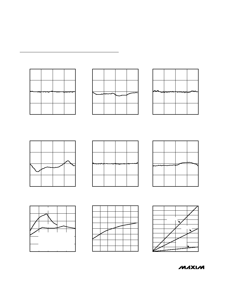
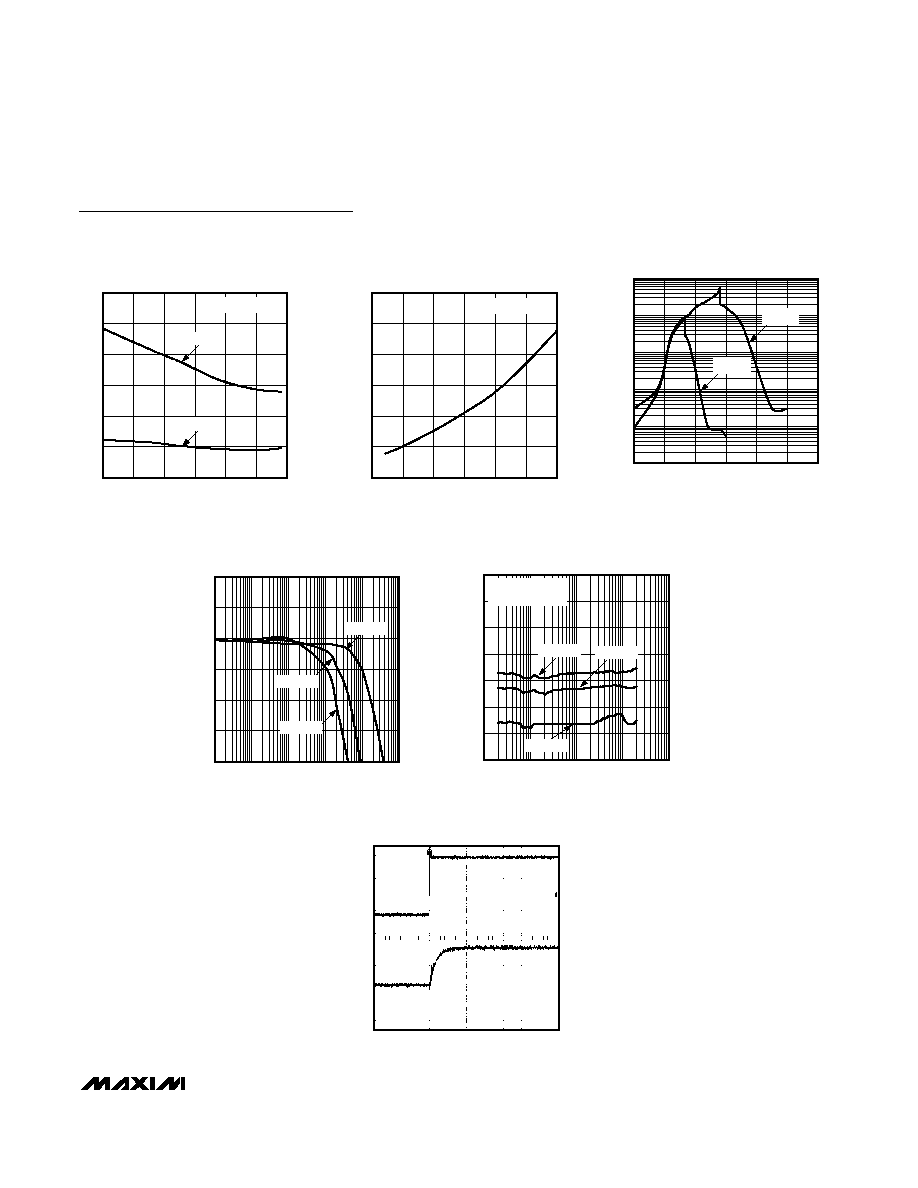
Typical Operating Characteristics
(V
DD
= +5.0V, T
A
= +25
°C, unless otherwise noted.)
MAX5527 R-DNL ERROR
vs. WIPER POSITION
MAX5527 toc01
WIPER POSITION
R-DNL ERROR (LSB)
48
32
16
-0.005
0
0.005
0.010
-0.010
0
64
MAX5527 R-INL ERROR
vs. WIPER POSITION
MAX5527 toc02
WIPER POSITION
R-INL ERROR (LSB)
48
32
16
-0.005
0
0.005
0.010
-0.010
0
64
MAX5528 R-DNL ERROR
vs. WIPER POSITION
MAX5527 toc03
WIPER POSITION
R-DNL ERROR (LSB)
48
32
16
-0.005
0
0.005
0.010
-0.010
0
64
MAX5528 R-INL ERROR
vs. WIPER POSITION
MAX5527 toc04
WIPER POSITION
R-INL ERROR (LSB)
48
32
16
-0.005
0
0.005
0.010
-0.010
0
64
MAX5529 R-DNL ERROR
vs. WIPER POSITION
MAX5527 toc05
WIPER POSITION
R-DNL ERROR (LSB)
48
32
16
-0.005
0
0.005
0.010
-0.010
0
64
MAX5529 R-INL ERROR
vs. WIPER POSITION
MAX5527 toc06
WIPER POSITION
R-INL ERROR (LSB)
48
32
16
-0.005
0
0.005
0.010
-0.010
0
64
WIPER RESISTANCE vs. WIPER VOLTAGE
MAX5527 toc07
WIPER VOLTAGE
WIPER RESISTANCE (
)
4
3
2
1
25
50
75
100
125
150
0
0
5
V
DD
= 3V
V
DD
= 5V
MAX5527: V
DD
= 5V, I
SOURCE
= 50
µA
V
DD
= 3V, I
SOURCE
= 30
µA
MAX5528: V
DD
= 5V, I
SOURCE
= 100
µA
V
DD
= 3V, I
SOURCE
= 60
µA
MAX5529: V
DD
= 5V,
ISOURCE
= 500
µA
V
DD
= 3V, I
SOURCE
= 300
µA
END-TO-END RESISTANCE PERCENTAGE
CHANGE vs. TEMPERATURE
MAX5527 toc08
TEMPERATURE (
°C)
END-TO-END RESISTANCE CHANGE (%)
85
60
-15
10
35
-0.3
-0.2
-0.1
0
0.1
0.2
0.3
0.4
-0.4
-40
110
W-TO-L RESISTANCE vs. WIPER POSITION
W-TO-L RESISTANCE (k
)
10
20
30
40
50
60
70
80
90
100
0
MAX5527 toc09
WIPER POSITION
48
32
16
0
64
MAX5527
MAX5528
MAX5529
MAX5527/MAX5528/MAX5529
One-Time Programmable, Linear-Taper Digital
Potentiometers
_______________________________________________________________________________________
5
STATIC SUPPLY CURRENT
vs. TEMPERATURE
MAX5527 toc10
TEMPERATURE (
°C)
SUPPLY CURRENT (nA)
85
60
35
10
-15
50
100
150
200
250
300
0
-40
110
V
DD
= 5V
V
DD
= 3V
CS = U/D = GND
STATIC SUPPLY CURRENT
vs. SUPPLY VOLTAGE
MAX5527 toc11
SUPPLY VOLTAGE (V)
SUPPLY CURRENT (nA)
5.0
4.5
4.0
3.5
3.0
50
100
150
200
250
300
0
2.5
5.5
CS = U/D = GND
SUPPLY CURRENT
vs. DIGITAL INPUT VOLTAGE
MAX5527 toc12
DIGTAL INPUT VOLTAGE (V)
SUPPLY CURRENT (
µ
A)
5
4
3
2
1
0.1
1
10
100
1000
0.01
0
6
V
DD
= 5V
V
DD
= 3V
MIDSCALE WIPER RESPONSE
vs. FREQUENCY
MAX5527 toc13
FREQUENCY (kHz)
GAIN (dB)
1000
100
10
1
-15
-12
-9
-6
-3
0
-18
0.1
10,000
MAX5527
MAX5528
MAX5529
TOTAL HARMONIC DISTORTION
vs. FREQUENCY
MAX5527 toc14
FREQUENCY (kHz)
THD (dB)
10
1
0.1
-100
-90
-80
-70
-60
-50
-40
-110
0.01
100
MAX5527
MAX5528
MAX5529
MIDSCALE, 1V
RMS
,
R
L
= 100k
TAP-TO-TAP SWITCHING TRANSIENT
MAX5527 toc15
400ns
U/
D
2V/div
GND
OUTPUT
W
50mV/div
Typical Operating Characteristics (continued)
(V
DD
= +5V, T
A
= +25°C, unless otherwise noted.)