General Description
The MAX5490 precision resistor-divider consists of two
accurately matched resistors with access to the ends
and center of the divider. This device offers excellent
resistance matching of 0.035% (A grade), 0.05% (B
grade), and 0.1% (C grade). The MAX5490 provides an
extremely low resistance-ratio temperature drift of
1ppm/°C (typ) over -40°C to +85°C, and has an end-to-
end resistance of 100k
. Resistance ratios from 1:1 to
100:1 are available. Five standard ratios are available
(see Table 1), and custom ratios are also available upon
request. The MAX5490 is ideal for precision gain-setting
applications where tight resistance matching and low
temperature drift are necessary.
The MAX5490 is available in a space-saving 3-pin
SOT23 package, and is guaranteed over the extended
-40°C to +85°C temperature range.
Applications
Industrial Process Control
Instrumentation
Precision Gain Setting
Medical Equipment
Automatic Test Equipment
Base Stations
Features
Resistance Ratios from 1:1 to 100:1
Custom Ratios Available Upon Request
Tight Initial Ratio Accuracy
0.035% (MAX5490A)
0.05% (MAX5490B)
0.1% (MAX5490C)
Low 1ppm/
°
C (typ) Resistor-Ratio-Drift
Up to 80V Operating Voltage Across Sum of R1
and R2
Tiny 3-Pin SOT23 Package
MAX5490
100k
Precision-Matched Resistor-Divider in
SOT23
________________________________________________________________ Maxim Integrated Products
1
P2
1
3
P3
P1
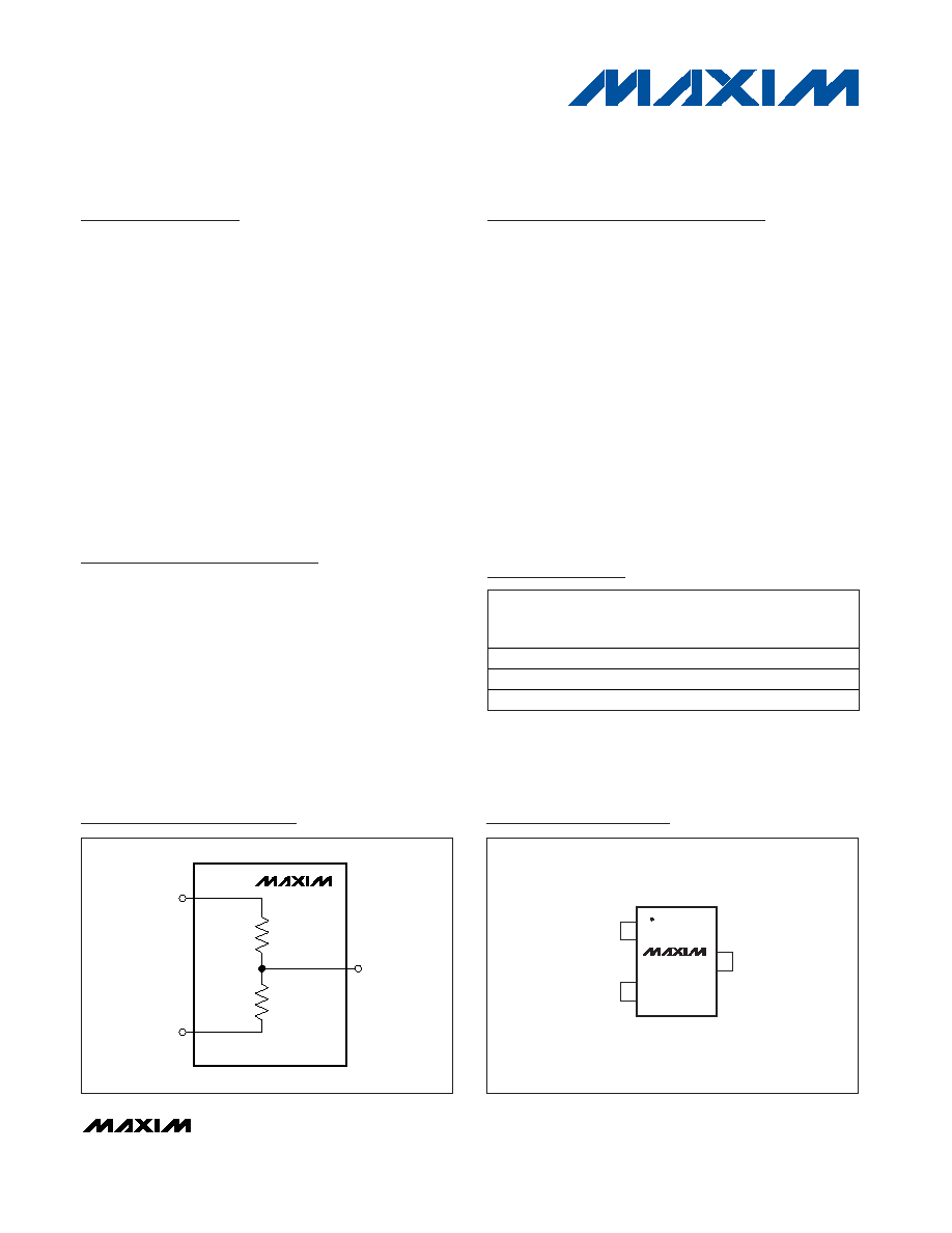
MAX5490
SOT23
TOP VIEW
2
Pin Configuration
Ordering Information*
P1
P2
P3
MAX5490
R
2
R
1
Block Diagram
19-3337; Rev 1; 8/04
For pricing, delivery, and ordering information, please contact Maxim/Dallas Direct! at
1-888-629-4642, or visit Maxim's website at www.maxim-ic.com.
*See the How to Order section for more details.
PA R T
T EM P
R A N G E
PIN -
PA C K A G E
R A T IO
A C C U R A C Y
( % )
M AX 5490
_
A
_ _ _ _ _
- T - 40° C to + 85°C 3
S
O T23- 3
0.035
M AX 5490
_
B
_ _ _ _ _
- T - 40° C to + 85°C 3
S
O T23- 3
0.05
M AX 5490
_
C
_ _ _ _ _
- T - 40° C to + 85°C 3
S
O T23- 3
0.1

MAX5490
100k
Precision-Matched Resistor-Divider in
SOT23
2
_______________________________________________________________________________________
ABSOLUTE MAXIMUM RATINGS
DC ELECTRICAL CHARACTERISTICS
(T
A
= -40°C to +85°C, unless otherwise noted. Typical values are at T
A
= +25°C.) (Note 1)
Stresses beyond those listed under "Absolute Maximum Ratings" may cause permanent damage to the device. These are stress ratings only, and functional
operation of the device at these or any other conditions beyond those indicated in the operational sections of the specifications is not implied. Exposure to
absolute maximum rating conditions for extended periods may affect device reliability.
Voltage Between P1 and P2.................................................100V
Maximum Current into Any Pin ......................................±1.00mA
Continuous Power Dissipation (T
A
= +70°C)
3-Pin SOT23 (derate 7.1mW/°C above +70°C).........571.4mW
3-Pin SOT23 (
J-A
) .....................................................141°C/W
Operating Temperature Range ...........................-40°C to +85°C
Junction Temperature ......................................................+150°C
Storage Temperature Range .............................-65°C to +150°C
Lead Temperature (soldering, 10s) .................................+300°C
PARAMETER
SYMBOL
CONDITIONS
MIN
TYP
MAX
UNITS
MAX5490_A, T
A
= +25°C
±0.035
MAX5490_B, T
A
= +25°C
±0.05
Initial Resistor Ratio Error (Note 2)
MAX5490_C, T
A
= +25°C
±0.1
%
1:1
ratio 10:1
1
2
Resistance-Ratio Temperature
Coefficient (Note 3)
10:1
ratio 25:1
2
4
ppm/°C
Absolute Temperature Coefficient
of Resistance
TCR
(Note 4)
35
ppm/°C
Voltage Coefficient of Resistance
VCR
(Note 5)
0.1
ppm/V
End-to-End Resistance (R
1
+ R
2
)
95
100
105
k
Continuous Working Voltage
Between P1 and P2
V
P1-P2
-80
+80
V
Continuous Current
I
R1
, I
R2
840
µA
P1, P2, P3 Capacitance
2
pF
Maximum Power Rating
67.2
mW
Resistance Ratio Long-Term
Stability
2000 hours at +70
°C
±0.03
%
-3dB Bandwidth
f
3dB
1:1 ratio (Note 6)
3
MHz
Thermal Noise
45
µV
RMS
Current Noise
In accordance with MIL-STD-2020
method 30B
-25
dB
Note 1:
The MAX5490 is 100% production tested at T
A
= +25°C. Specifications over -40°C to +85°C are guaranteed by design and
characterization.
Note 2:
Testing conditions: T
A
= +25°C, V
P1-P2
= 10V and 80V.
Note 3:
Resistance-ratio temperature coefficient is defined as
For ratios from 25:1 to 100:1, contact factory.
Note 4:
Absolute TCR is defined as
R
R
R
R
T
1
2
1
2
×
R
R
R
R
T
1
2
1
2
+
(
)
+
(
)
×
and is guaranteed by design, not production tested.
and is tested at 10V and 80V.
MAX5490
100k
Precision-Matched Resistor-Divider in
SOT23
_______________________________________________________________________________________
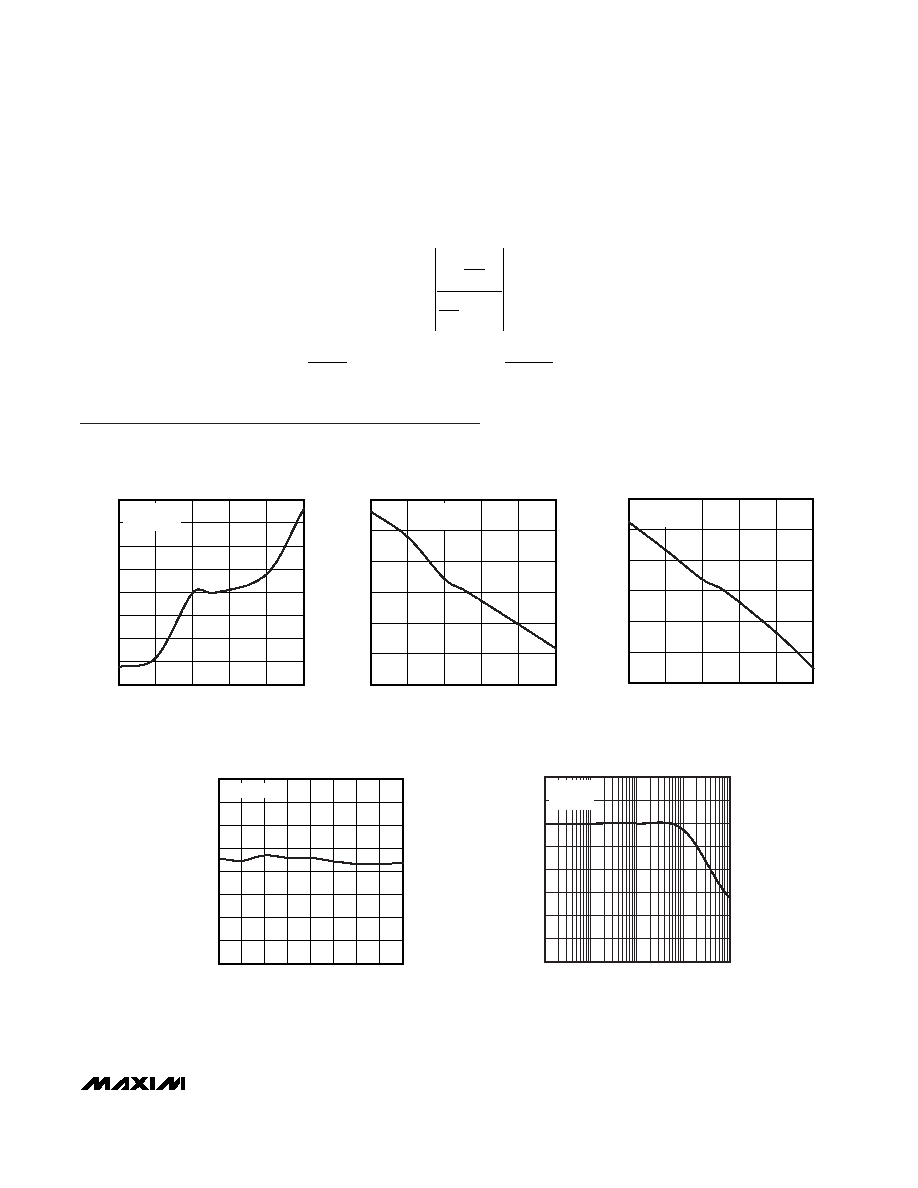
3
-20
-15
-10
-5
0
5
10
15
20
-40
-15
10
35
60
85
NORMALIZED RESISTANCE-RATIO DRIFT
vs. TEMPERATURE
MAX5490 toc01
TEMPERATURE (
°C)
RATIO DRIFT (ppm)
V
P1-P2
= 10V
RATIO 1:1
-120
-40
-80
40
0
80
120
-40
10
-15
35
60
85
NORMALIZED RESISTANCE-RATIO DRIFT
vs. TEMPERATURE
MAX5490 toc02
TEMPERATURE (
°C)
RATIO DRIFT (ppm)
V
P1-P2
= 10V
RATIO 10:1
-150
-50
-100
50
0
100
150
-40
10
-15
35
60
85
NORMALIZED RESISTANCE-RATIO DRIFT
vs. TEMPERATURE
MAX5490 toc03
TEMPERATURE (
°C)
RATIO DRIFT (ppm)
V
P1-P2
= 10V
RATIO 25:1
-0.04
-0.03
-0.02
-0.01
0
0.01
0.02
0.03
0.04
0
20
40
60
70
10
30
50
80
RESISTANCE-RATIO ACCURACY
vs. VOLTAGE
MAX5490 toc04
VOLTAGE (V)
RATIO ACCURACY (%)
RATIO 25:1
0.1
10
1
100
1000
FREQUENCY RESPONSE
MAX5490 toc05
FREQUENCY (kHz)
RESPONSE (dB)
6
-18
-12
-9
-3
3
-15
-6
0
1:1 RATIO
C
L
= 10pF
Typical Operating Characteristics
(V
P1-P2
= 10V, T
A
= +25°C, unless otherwise noted.)
Note 5:
Resistance-ratio voltage coefficient is defined as
R
R
R
R
V
1
2
1
2
×
and is guaranteed by design, not production tested.
Note 6:
Calculate bandwidth by using
1
2
RC
,
where C = C
P3
and
R
R
R
R
R
=
×
+
1
2
1
2
.
DC ELECTRICAL CHARACTERISTICS (continued)
(T
A
= -40°C to +85°C, unless otherwise noted. Typical values are at T
A
= +25°C.) (Note 1)
MAX5490
100k
Precision-Matched Resistor-Divider in
SOT23
4
_______________________________________________________________________________________
Detailed Description
As shown in the Block Diagram, the MAX5490 consists
of two precision, low-ratio-drift resistors with an end-to-
end resistance of 100k
(R
1
+ R
2
). P3 is the set point
of the divider. The maximum working voltage of the
MAX5490 is 80V. This device offers a wide range of
resistance ratios (R
1
/R
2
) from 1:1 to 100:1 and is ideal
for precision operational amplifier gain/attenuation con-
trol. A maximum initial ratio accuracy of 0.035% and a
low 1ppm/
°C ratio drift enhance system accuracy.
Applications Information
Self-Heating and Error
Applying a voltage across terminals P1 and P2 causes
the device to heat up due to power dissipation. In high-
voltage applications, consider the error in resistance-
ratio temperature coefficient caused by self-heating.
The worst-case self-heating occurs when the operating
voltage attains its maximum value. Approximate the
result of power dissipation under this condition as:
The thermal resistance from junction to ambient,
J-A
,
for a 3-pin SOT23 package is 141°C/W. Calculate the
resulting temperature rise as:
T = 64mW x 141°C/W = 9.02°C
If the ratio temperature coefficient is 1ppm/°C (typ), the
total error introduced by self-heating is:
9.02
°C x 1ppm/°C = 9.02ppm
P
V
R
V
k
mW
DISS
MAX
=
(
)
=
( )
=
2
2
80
100
64
Pin Description
PIN
NAME
FUNCTION
1
P1
R
1
Connection Terminal
2
P2
R
2
Connection Terminal
3
P3
Set-Point Connection Terminal
1000
10
1
100
1k
100
FREQUENCY (Hz)
NOISE (nV/
Hz
)
10
SPECTRAL NOISE DENSITY
MAX5490 toc06
RATIO 1:1
SIGNAL CONNECTED TO P2
P1 GROUNDED
V
P1-P2
= 10V
V
P1-P2
= 2V
100
10
1
0.1
0.01
0.001
0.0001
10
1k
10k
100
100k
THD+N RESPONSE
MAX5490 toc07
FREQUENCY (Hz)
THD+N (%)
1:1 RATIO
20Hz TO 20kHz BANDPASS
Typical Operating Characteristics (continued)
(V
P1-P2
= 10V, T
A
= +25°C, unless otherwise noted.)
MAX5490
100k
Precision-Matched Resistor-Divider in
SOT23
_______________________________________________________________________________________
5
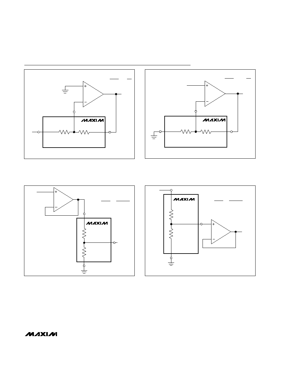
IN
P1
P2
P3
MAX5490
R
2
R
1
OUT
Figure 3. Buffered Attenuator
MAX5490
R
2
R
1
P1
P2
P3
IN
OUT
Figure 1. Inverting Amplifier Configuration
P1
P2
P3
MAX5490
R
2
R
1
OUT
IN
Figure 4. Attenuator with Buffer
MAX5490
R
2
R
1
P1
P2
P3
IN
OUT
Figure 2. Noninverting Amplifier Configuration
A
V
V
R
R
OUT
IN
=
= -
1
2
A
V
V
R
R
OUT
IN
=
=
+
1
1
2
A
V
V
R
R
R
OUT
IN
=
=
+
2
1
2
A
V
V
R
R
R
OUT
IN
=
=
+
2
1
2
Typical Applications