General Description
The MAX5487/MAX5488/MAX5489 dual, linear-taper,
digital potentiometers function as mechanical poten-
tiometers with a simple 3-wire SPITM-compatible digital
interface that programs the wipers to any one of 256
tap positions. These digital potentiometers feature a
nonvolatile memory (EEPROM) to return the wipers to
their previously stored positions upon power-up.
The MAX5487 has an end-to-end resistance of 10k
,
while the MAX5488 and MAX5489 have resistances of
50k
and 100k, respectively. These devices have a
low 35ppm/°C end-to-end temperature coefficient, and
operate from a single +2.7V to +5.25V supply.
The MAX5487/MAX5488/MAX5489 are available in a
16-pin 3mm x 3mm x 0.8mm thin QFN package. Each
device is guaranteed over the extended -40
°C to +85°C
temperature range.
Applications
LCD Screen Adjustment
Audio Volume Control
Mechanical Potentiometer Replacement
Low-Drift Programmable Filters
Low-Drift Programmable-Gain Amplifiers
Features
o Wiper Position Stored in Nonvolatile Memory
(EEPROM) and Recalled Upon Power-Up or
Recalled by an Interface Command
o 3mm x 3mm x 0.8mm Thin QFN Package
o ±1 LSB INL, ±0.5 LSB DNL (Voltage-Divider Mode)
o 256 Tap Positions
o 35ppm/°C End-to-End Resistance Temperature
Coefficient
o 5ppm/°C Ratiometric Temperature Coefficient
o 10k, 50k, and 100k End-to-End Resistance
Values
o SPI-Compatible Serial Interface
o Reliability
200,000 Wiper Store Cycles
50-Year Wiper Data Retention
o +2.7V to +5.25V Single-Supply Operation
MAX5487/MAX5488/MAX5489
Dual, 256-Tap, Nonvolatile, SPI-Interface,
Linear-Taper Digital Potentiometers
________________________________________________________________ Maxim Integrated Products
1
19-3478; Rev 1; 1/05
For pricing, delivery, and ordering information, please contact Maxim/Dallas Direct! at
1-888-629-4642, or visit Maxim's website at www.maxim-ic.com.
SPI is a trademark of Motorola, Inc.
Ordering Information/Selector Guide
PART
TEMP RANGE
PIN-PACKAGE
END-TO-END
RESISTANCE (k
)
TOP MARK
MAX5487ETE*
-40
°C to +85°C
16 Thin QFN-EP**
10
ABR
MAX5488ETE
-40
°C to +85°C
16 Thin QFN-EP**
50
ABS
MAX5489ETE
-40
°C to +85°C
16 Thin QFN-EP**
100
ABT
*Future product--contact factory for availability.
**EP = Exposed pad.
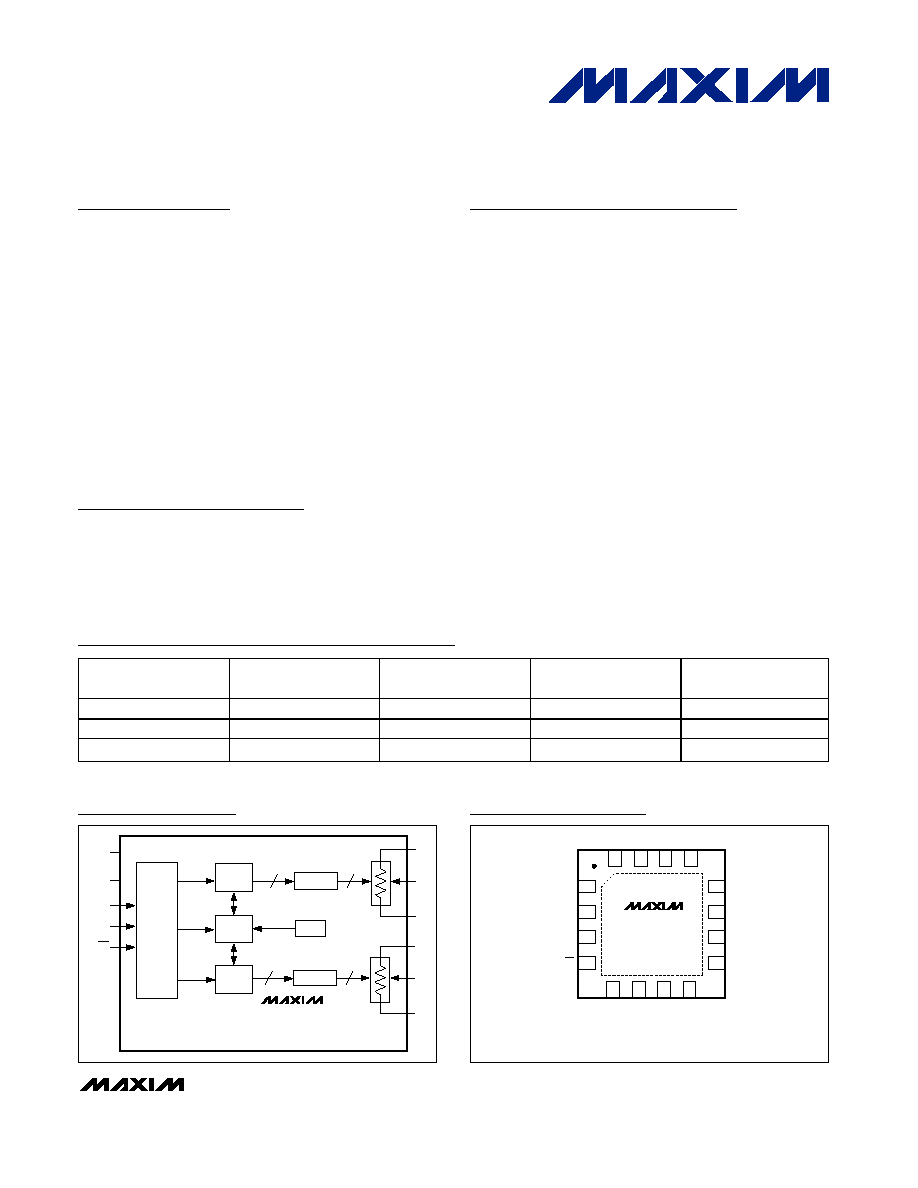
MAX5487
MAX5488
MAX5489
POR
8-BIT
LATCH
16-BIT
NV RAM
SCLK
DIN
CS
DECODER
8
8
256
DECODER
256
HA
WA
LA
HB
WB
LB
V
DD
GND
SPI
INTERFACE
8-BIT
LATCH
Functional Diagram
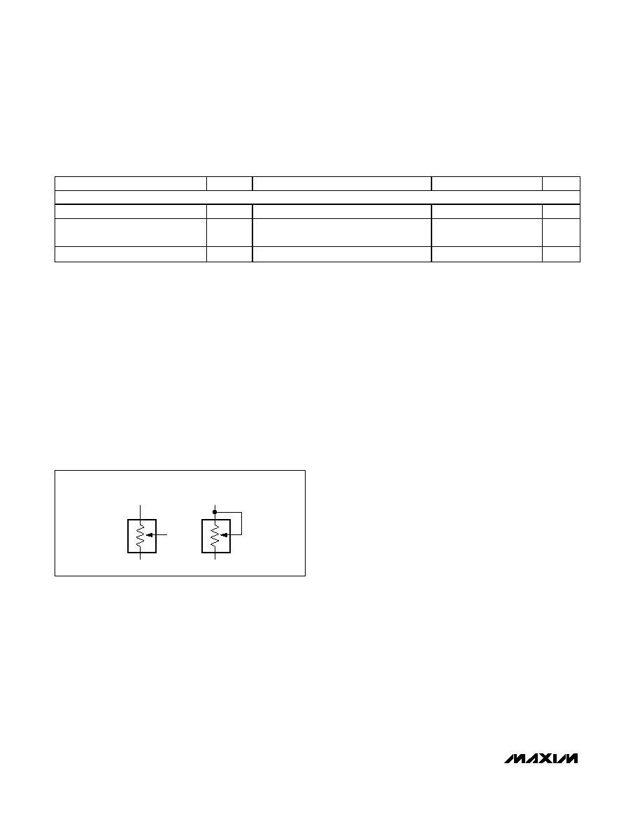
16
1
2
3
4
12
11
10
9
15
14
13
5
6
7
8
N.C.
HA
WA
LA
HB
WB
LB
N.C.
SCLK
DIN
N.C.
N.C.
GND
N.C.
V
DD
TOP VIEW
EXPOSED PAD CONNECTED TO GND.
MAX5487
MAX5488
MAX5489
CS
THIN QFN
3mm
× 3mm
Pin Configuration

MAX5487/MAX5488/MAX5489
Dual, 256-Tap, Nonvolatile, SPI-Interface,
Linear-Taper Digital Potentiometers
2
_______________________________________________________________________________________
ABSOLUTE MAXIMUM RATINGS
Stresses beyond those listed under "Absolute Maximum Ratings" may cause permanent damage to the device. These are stress ratings only, and functional
operation of the device at these or any other conditions beyond those indicated in the operational sections of the specifications is not implied. Exposure to
absolute maximum rating conditions for extended periods may affect device reliability.
V
DD
to GND ...........................................................-0.3V to +6.0V
All Other Pins
to GND......................-0.3V to the lower of (V
DD
+ 0.3V) and +6.0V
Maximum Continuous Current into H_, W_, and L_
MAX5487......................................................................
±5.0mA
MAX5488......................................................................
±1.3mA
MAX5489......................................................................
±0.6mA
Continuous Power Dissipation (T
A
= +70
°C)
16-Pin Thin QFN (derate 17.5mW/
°C above +70°C).....1398mW
Operating Temperature Range ...........................-40
°C to +85°C
Junction Temperature ......................................................+150
°C
Storage Temperature Range .............................-60
°C to +150°C
Lead Temperature (soldering, 10s) .................................+300
°C
DC ELECTRICAL CHARACTERISTICS
(V
DD
= +2.7V to +5.25V, V
H
= V
DD
, V
L
= GND, T
A
= -40
°C to +85°C, unless otherwise noted. Typical values are at V
DD
= +5.0V,
T
A
= +25
°C, unless otherwise noted.) (Note 1)
PARAMETER
SYMBOL
CONDITIONS
MIN
TYP
MAX
UNITS
DC PERFORMANCE (Voltage-Divider Mode, Figure 1)
Resolution
N
256
Taps
Integral Nonlinearity
INL
(Note 2)
±1
LSB
Differential Nonlinearity
DNL
(Note 2)
±0.5
LSB
Dual-Code Matching
Register A = register B
2
LSB
End-To-End Resistor Tempco
TC
R
35
ppm/°C
Ratiometric Resistor Tempco
5
ppm/°C
MAX5488
-0.6
+1.2
Full-Scale Error
MAX5489
-0.3
+1.2
LSB
MAX5488
0.6
1.5
Zero-Scale Error
MAX5489
0.3
1
LSB
DC PERFORMANCE (Variable-Resistor Mode, Figure 1)
Resolution
256
Taps
V
DD
= 5.0V
±1.5
Integral Nonlinearity (Note 3)
MAX5488/MAX5489
V
DD
= 3.0V
±3
V
DD
= 5.0V
±1
Differential Nonlinearity (Note 3)
MAX5488/MAX5489
V
DD
= 3.0V
±1
LSB
DC PERFORMANCE (Resistor Characteristics)
V
DD
= 5.0V
200
350
Wiper Resistance (Note 4)
R
W
V
DD
= 3.0V
325
675
Wiper Capacitance
C
W
50
pF
MAX5487
7.5
10
12.5
MAX5488
37.5
50
62.5
End-to-End Resistance
R
HL
MAX5489
75
100
125
k

MAX5487/MAX5488/MAX5489
Dual, 256-Tap, Nonvolatile, SPI-Interface,
Linear-Taper Digital Potentiometers
_______________________________________________________________________________________
3
DC ELECTRICAL CHARACTERISTICS (continued)
(V
DD
= +2.7V to +5.25V, V
H
= V
DD
, V
L
= GND, T
A
= -40
°C to +85°C, unless otherwise noted. Typical values are at V
DD
= +5.0V,
T
A
= +25
°C, unless otherwise noted.) (Note 1)
PARAMETER
SYMBOL
CONDITIONS
MIN
TYP
MAX
UNITS
DIGITAL INPUTS
V
DD
= 3.6V to 5.25V
2.4
Input High Voltage (Note 5)
V
IH
V
DD
= 2.7V to 3.6V
0.7 x
V
DD
V
Input Low Voltage
V
IL
V
DD
= 2.7V to 5.25V (Note 5)
0.8
V
Input Leakage Current
I
IN
±1.0
µA
Input Capacitance
C
IN
5.0
pF
AC PERFORMANCE
Crosstalk
f
H_
= 1kHz, L_ = GND, measurement at W_
(Note 6)
-90
dB
MAX5488
90
-3dB Bandwidth
BW
Wiper at midscale
C
W_
= 10pF
MAX5489
45
kHz
Total Harmonic Distortion
THD
V
H_
= 1V
RMS
at 1kHz, L_ = GND,
measurement at W_
0.02
%
TIMING CHARACTERISTICS (Analog)
MAX5488
0.75
Wiper-Settling Time
t
S
Code 0 to 127
(Note 7)
MAX5489
1.5
µs
TIMING CHARACTERISTICS (Digital, Figure 2, Note 8)
SCLK Frequency
5
MHz
SCLK Clock Period
t
CP
200
ns
SCLK Pulse-Width High
t
CH
80
ns
SCLK Pulse-Width Low
t
CL
80
ns
CS Fall to SCLK Rise Setup
t
CSS
80
ns
SCLK Rise to
CS Rise Hold
t
CSH
0
ns
DIN to SCLK Setup
t
DS
50
ns
DIN Hold after SCLK
t
DH
0
ns
SCLK Rise to
CS Fall Delay
t
CS0
20
ns
CS Rise to SCLK Rise Hold
t
CS1
80
ns
CS Pulse-Width High
t
CSW
200
ns
Write NV Register Busy Time
t
BUSY
12
ms
Read NV Register Access Time
t
ACC
1
µs
W r i te W i p er Reg i ster to O utp ut D el ay
t
WO
1
µs
NONVOLATILE MEMORY RELIABILITY
T
A
= +85°C
50
Data Retention
Mil-Std-883 test
method 1008
T
A
= +125°C
10
Years
T
A
= +85°C
200,000
Endurance
Mil-Std-883 test
method 1033
T
A
= +125°C
50,000
Stores
MAX5487/MAX5488/MAX5489
Dual, 256-Tap, Nonvolatile, SPI-Interface,
Linear-Taper Digital Potentiometers
4
_______________________________________________________________________________________
Note 1: All devices are production tested at T
A
= +25°C and are guaranteed by design and characterization for -40°C < T
A
< +85°C.
Note 2: DNL and INL are measured with the potentiometer configured as a voltage-divider with H_ = V
DD
and L_ = 0. The wiper terminal
is unloaded and measured with an ideal voltmeter.
Note 3: DNL and INL are measured with the potentiometer configured as a variable resistor. H_ is unconnected and L_ = 0. For V
DD
=
+5V, the wiper terminal is driven with a source current of 400µA for the 10k
configuration, 80µA for the 50k configuration,
and 40µA for the 100k
configuration. For V
DD
= +3V, the wiper terminal is driven with a source current of 200µA for the 10k
configuration, 40µA for the 50k
configuration, and 20µA for the 100k configuration.
Note 4: The wiper resistance is the worst value measured by injecting the currents given in Note 3 into W_ with L_ = GND. R
W
=
(V
W
- V
H
) / I
W
.
Note 5: The device draws higher supply current when the digital inputs are driven with voltages between (V
DD
- 0.5V) and (GND +
0.5V). See Supply Current vs. Digital Input Voltage in the Typical Operating Characteristics section.
Note 6: Wiper at midscale with a 10pF load.
Note 7: Wiper-settling time is the worst-case 0-to-50% rise time, measured between tap 0 and tap 127. H_ = V
DD
, L_ = GND, and
the wiper terminal is unloaded and measured with a 10pF oscilloscope probe (see Tap-to-Tap Switching Transient in the
Typical Operating Characteristics section).
Note 8: Digital timing is guaranteed by design and characterization, and is not production tested.
DC ELECTRICAL CHARACTERISTICS (continued)
(V
DD
= +2.7V to +5.25V, V
H
= V
DD
, V
L
= GND, T
A
= -40
°C to +85°C, unless otherwise noted. Typical values are at V
DD
= +5.0V,
T
A
= +25
°C, unless otherwise noted.) (Note 1)
PARAMETER
SYMBOL
CONDITIONS
MIN
TYP
MAX
UNITS
POWER SUPPLIES
Power-Supply Voltage
V
DD
2.70
5.25
V
Supply Current
I
DD
During write cycle only, digital inputs =
V
DD
or GND
400
µA
Standby Current
Digital inputs = V
DD
or GND, T
A
= +25°C
0.5
1
µA
H
L
W
VOLTAGE-DIVIDER
CONFIGURATION
VARIABLE-RESISTOR
CONFIGURATION
H
L
Figure 1. Voltage-Divider/Variable-Resistor Configurations
MAX5487/MAX5488/MAX5489
Dual, 256-Tap, Nonvolatile, SPI-Interface,
Linear-Taper Digital Potentiometers
_______________________________________________________________________________________
5
SUPPLY CURRENT vs. TEMPERATURE
MAX5487-89 toc01
TEMPERATURE (
°C)
SUPPLY CURRENT (
µ
A)
60
35
10
-15
0.2
0.4
0.6
0.8
1.0
1.2
0
-40
85
V
CC
= 5V
V
CC
= 3V
SUPPLY CURRENT
vs. DIGITAL INPUT VOLTAGE
MAX5487-89 toc02
DIGITAL INPUT VOLTAGE (V)
SUPPLY CURRENT (
µ
A)
4
3
2
1
1
10
100
1000
10,000
0
0
5
V
CC
= 5V
V
CC
= 3V
0
100
200
300
400
0
64
128
192
32
96
160
224
256
WIPER RESISTANCE
vs. TAP POSITION (MAX5488)
MAX5487-89toc03
TAP POSITION
WIPER RESISTANCE (
)
TAP-TO-TAP SWITCHING TRANSIENT
(MAX5488)
MAX5487-89 toc04
1.0
µs/div
WIPER
20mV/div
V
H_
= 5.0V
CS
2.0V/div
TAP-TO-TAP SWITCHING TRANSIENT
(MAX5489)
MAX5487-89 toc05
1.0
µs/div
WIPER
20mV/div
V
H_
= 5.0V
CS
2.0V/div
WIPER TRANSIENT AT POWER-ON
MAX5487-89 toc06
2.0
µs/div
WIPER
2.0V/div
V
H_
= V
DD
V
DD
2.0V/div
Typical Operating Characteristics
(V
DD
= +5.0V, T
A
= +25
°C, unless otherwise noted.)