
General Description
The MAX5481MAX5484 10-bit (1024-tap) nonvolatile,
linear-taper, programmable voltage-dividers and vari-
able resistors perform the function of a mechanical
potentiometer, but replace the mechanics with a pin-
configurable 3-wire serial SPITM-compatible interface or
up/down digital interface. The MAX5481/MAX5482 are
3-terminal voltage-dividers and the MAX5483/MAX5484
are 2-terminal variable resistors.
The MAX5481MAX5484 feature an internal, non-
volatile, electrically erasable programmable read-only
memory (EEPROM) that stores the wiper position for ini-
tialization during power-up. The 3-wire SPI-compatible
serial interface allows communication at data rates up
to 7MHz. A pin-selectable up/down digital interface is
also available.
The MAX5481MAX5484 are ideal for applications
requiring digitally controlled potentiometers. Two end-to-
end resistance values are available (10k
and 50k) in a
voltage-divider or a variable-resistor configuration (see
the Selector Guide). The nominal resistor temperature
coefficient is 35ppm/°C end-to-end, and only 5ppm/°C
ratiometric, making these devices ideal for applications
requiring low-temperature-coefficient voltage-dividers,
such as low-drift, programmable gain-amplifiers.
The MAX5481MAX5484 operate with either a +2.7V to
+5.25V single power supply or ±2.5V dual power sup-
plies. These devices consume 400µA (max) of supply
current when writing data to the nonvolatile memory
and 1.0µA (max) of standby supply current. The
MAX5481MAX5484 are available in a space-saving
(3mm x 3mm), 16-pin TQFN, or a 14-pin TSSOP pack-
age and are specified over the extended (-40°C to
+85°C) temperature range.
Applications
Features
1024 Tap Positions
Power-On Recall of Wiper Position from
Nonvolatile Memory
16-Pin (3mm x 3mm x 0.8mm) TQFN or 14-Pin
TSSOP Package
35ppm/°C End-to-End Resistance Temperature
Coefficient
5ppm/°C Ratiometric Temperature Coefficient
10k and 50k End-to-End Resistor Values
Pin-Selectable SPI-Compatible Serial Interface or
Up/Down Digital Interface
1µA (max) Standby Current
Single +2.7V to +5.25V Supply Operation
Dual ±2.5V Supply Operation
MAX5481MAX5484
10-Bit, Nonvolatile, Linear-Taper Digital
Potentiometers
________________________________________________________________ Maxim Integrated Products
1
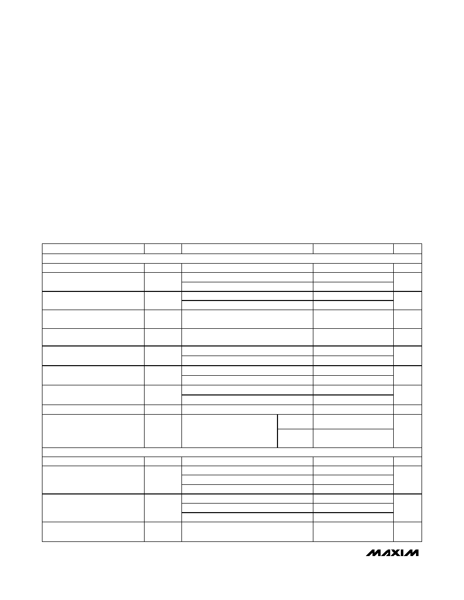
Ordering Information
16
15
14
13
V
SS
N.C.
V
DD
GND
9
10
11
12
SPI/
UD
DIN(U/
D
)
SCLK(
INC
)
CS
4
3
2
1
N.C.
L
W
H
5
6
7
8
N.C.
N.C.
N.C.
V
SS
INTERFACE
TOP VIEW
TQFN
*SEE FUNCTIONAL DIAGRAM
16
15
14
13
V
SS
N.C.
V
DD
GND
9
10
11
12
SPI/
UD
DIN(U/
D
)
SCLK(
INC
)
CS
4
3
2
1
N.C.
L
W
D.N.C.
5
6
7
8
N.C.
N.C.
N.C.
V
SS
MAX5483
MAX5484
INTERFACE
TQFN
MAX5481*
MAX5482*
Pin Configurations
19-3708; Rev 0; 5/05
For pricing, delivery, and ordering information, please contact Maxim/Dallas Direct! at
1-888-629-4642, or visit Maxim's website at www.maxim-ic.com.
PART
PIN-PACKAGE
PKG CODE
TOP
MARK
MAX5481ETE
16 TQFN-EP**
T1633F-3
ACP
MAX5481EUD*
14 TSSOP
--
--
Selector Guide appears at end of data sheet.
SPI is a trademark of Motorola, Inc.
All devices are specified over the -40°C to +85°C operating
temperature range.
*Future product--contact factory for availability.
**EP = Exposed pad.
Ordering Information continued at end of data sheet.
Pin Configurations continued at end of data sheet.
Gain and Offset
Adjustment
LCD Contrast Adjustment
Pressure Sensors
Low-Drift Programmable
Gain Amplifiers
Mechanical Potentiometer
Replacement
MAX5481MAX5484
10-Bit, Nonvolatile, Linear-Taper Digital
Potentiometers
2
_______________________________________________________________________________________
ABSOLUTE MAXIMUM RATINGS
Stresses beyond those listed under "Absolute Maximum Ratings" may cause permanent damage to the device. These are stress ratings only, and functional
operation of the device at these or any other conditions beyond those indicated in the operational sections of the specifications is not implied. Exposure to
absolute maximum rating conditions for extended periods may affect device reliability.
V
DD
to GND ...........................................................-0.3V to +6.0V
V
SS
to GND............................................................-6.0V to +0.3V
V
DD
to V
SS
.............................................................-0.3V to +6.0V
H, L, W to V
SS
..................................(V
SS
- 0.3V) to (V
DD
+ 0.3V)
CS, SCLK(INC), DIN(U/D), SPI/UD to GND ..-0.3V to (V
DD
+ 0.3V)
Maximum Continuous Current into H, L, and W
MAX5481/MAX5483.........................................................±5mA
MAX5482/MAX5484......................................................±1.0mA
Maximum Current into Any Other Pin ...............................±50mA
Continuous Power Dissipation (T
A
= +70°C)
16-Pin TQFN (derate 17.5mW/°C above +70°C) .....1398.6mW
14-Pin TSSOP (derate 9.1mW/°C above +70°C) ..........727mW
Operating Temperature Range ...........................-40°C to +85°C
Junction Temperature ......................................................+150°C
Storage Temperature Range .............................-60°C to +150°C
Lead Temperature (soldering, 10s) .................................+300°C
ELECTRICAL CHARACTERISTICS
(V
DD
= +2.7V to +5.25V, V
SS
= GND = 0, V
H
= V
DD
, V
L
= 0, T
A
= -40°C to +85°C, unless otherwise noted. Typical values are at V
DD
= +5.0V, T
A
= +25°C, unless otherwise noted.) (Note 1)
PARAMETER
SYMBOL
CONDITIONS
MIN
TYP
MAX
UNITS
DC PERFORMANCE (MAX5481/MAX5482 programmable voltage-divider)
Resolution
N
10
Bits
V
DD
= 2.7V
±2
Integral Nonlinearity (Note 2)
INL
V
DD
= 5V
±2
LSB
V
DD
= 2.7V
±1
Differential Nonlinearity (Note 2)
DNL
V
DD
= 5V
±1
LSB
End-to-End Resistance
Temperature Coefficient
TC
R
35
ppm/°C
Ratiometric Resistance
Temperature Coefficient
5
ppm/°C
MAX5481
-4
-2.5
0
Full-Scale Error
FSE
MAX5482
-4
-0.75
0
LSB
MAX5481
0
+3.3
+5
Zero-Scale Error
ZSE
MAX5482
0
+1.45
+5
LSB
MAX5481
7.5
10
12.5
End-to-End Resistance
R
H-L
MAX5482
37.5
50
62.5
k
Wiper Capacitance
C
W
60
pF
MAX5481
6.3
Resistance from W to L and H
W at code = 15, H and L
shorted to V
SS
, measure
resistance from W to H, Figures
1 and 2
MAX5482
25
k
DC PERFORMANCE (MAX5483/MAX5484 variable resistor)
Resolution
N
10
Bits
V
DD
= 2.7V
-1.6
V
DD
= 3V
-4
-1.4
+4
Integral Nonlinearity (Note 3)
INL_R
V
DD
= 5V
-4
-1.3
+4
LSB
V
DD
= 2.7V
+0.45
V
DD
= 3V
-1
+0.4
+1
Differential Nonlinearity (Note 3)
DNL_R
V
DD
= 5V
-1
+0.35
+1
LSB
Variable-Resistor Temperature
Coefficient
TC
VR
V
DD
= 3V to 5.25V; code = 128 to 1024
35
ppm/°C
MAX5481MAX5484
10-Bit, Nonvolatile, Linear-Taper Digital
Potentiometers
_______________________________________________________________________________________
3
ELECTRICAL CHARACTERISTICS (continued)
(V
DD
= +2.7V to +5.25V, V
SS
= GND = 0, V
H
= V
DD
, V
L
= 0, T
A
= -40°C to +85°C, unless otherwise noted. Typical values are at V
DD
= +5.0V, T
A
= +25°C, unless otherwise noted.) (Note 1)
PARAMETER
SYMBOL
CONDITIONS
MIN
TYP
MAX
UNITS
MAX5483
7.5
10
12.5
k
Full-Scale Wiper-to-End
Resistance
R
W-L
MAX5484
37.5
50
62.5
k
MAX5483
70
Zero-Scale Resistor Error
R
Z
Code = 0
MAX5484
110
Wiper Resistance
R
W
V
DD
3V (Note 4)
50
Wiper Capacitance
C
W
60
pF
DIGITAL INPUTS (CS, SCLK(INC), DIN(U/D), SPI/UD) (Note 5)
V
DD
= +3.6V to
+5.25V
2.4
Single-supply operation
V
DD
= +2.7V to
+3.6V
0.7 x
V
DD
Input-High Voltage
V
IH
Dual-supply operation
V
DD
= +2.5V, V
SS
= -2.5V
2.0
V
Single-supply operation
V
DD
= +2.7V to
+5.25V
0.8
Input-Low Voltage
V
IL
Dual-supply operation
V
DD
= +2.5V, V
SS
= -2.5V
0.6
V
Input Leakage Current
I
IN
±1
µA
Input Capacitance
C
IN
5
pF
DYNAMIC CHARACTERISTICS
MAX5481
250
Wiper -3dB Bandwidth
Wiper at code = 01111
01111, C
LW
= 10pF
MAX5482
50
kHz
MAX5481
0.026
Total Harmonic Distortion
THD
V
DD
= 3V, wiper at
code = 01111 01111,
1V
RMS
at 10kHz is
applied at H, 10pF
load on W
MAX5482
0.03
%
NONVOLATILE MEMORY RELIABILITY
Data Retention
T
A
= +85°C
50
Years
T
A
= +25°C
200,000
Endurance
T
A
= +85°C
50,000
Stores
POWER SUPPLY
Single-Supply Voltage
V
DD
V
SS
= GND = 0
2.70
5.25
V
V
DD
GND = 0
2.50
5.25
Dual-Supply Voltage
V
SS
V
DD
- V
SS
5.25V
-2.5
-0.2
V
Average Programming Current
I
PG
During nonvolatile write; digital inputs =
V
DD
or GND
220
400
µA
Peak Programming Current
During nonvolatile write only; digital inputs
= V
DD
or GND
4
mA
Standby Current
I
DD
Digital inputs = V
DD
or GND, T
A
= +25°C
0.6
1
µA
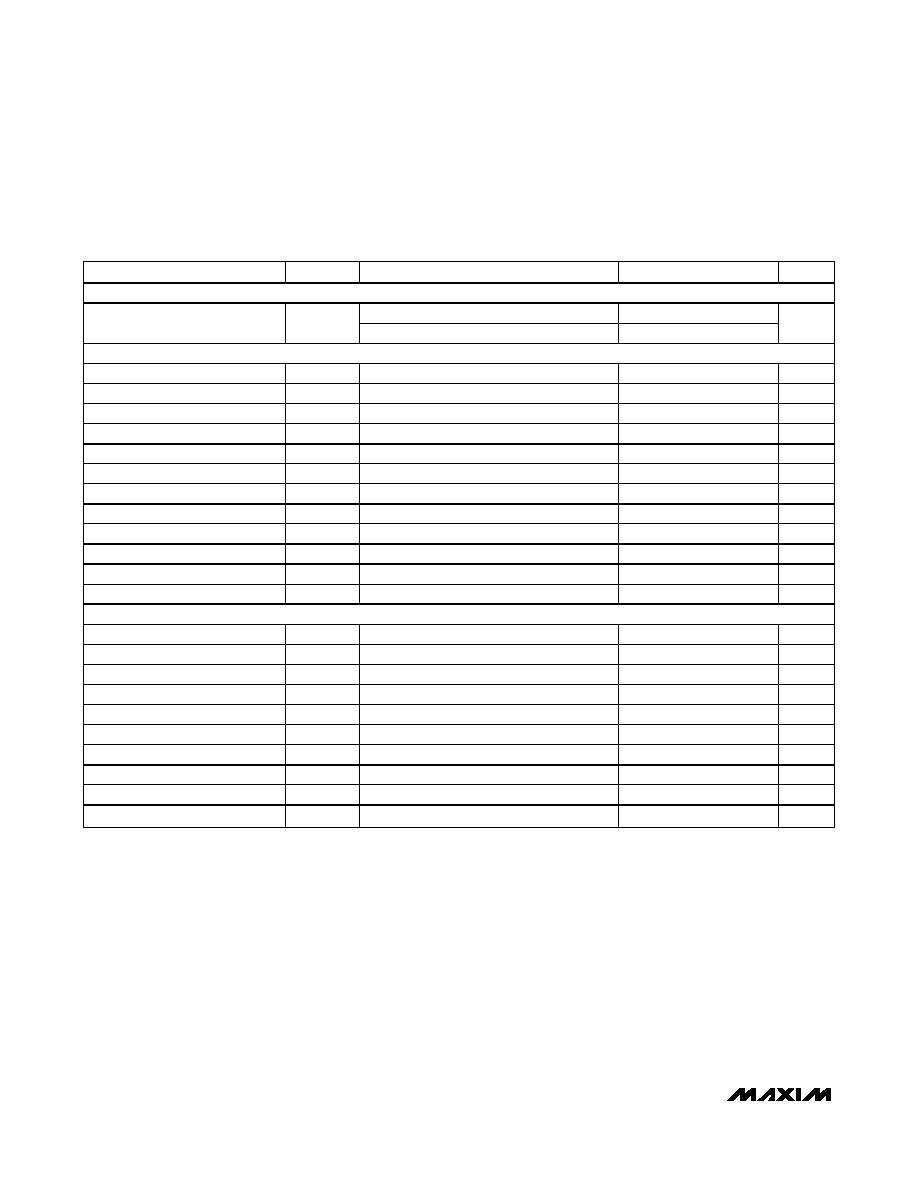
MAX5481MAX5484
10-Bit, Nonvolatile, Linear-Taper Digital
Potentiometers
4
_______________________________________________________________________________________
TIMING CHARACTERISTICS
(V
DD
= +2.7V to +5.25V, V
SS
= GND = 0, V
H
= V
DD
, V
L
= 0, T
A
= -40°C to +85°C, unless otherwise noted. Typical values are at V
DD
= +5.0V, T
A
= +25°C, unless otherwise noted.) (Note 1)
PARAMETER
SYMBOL
CONDITIONS
MIN
TYP
MAX
UNITS
ANALOG SECTION
MAX5481
5
Wiper Settling Time (Note 6)
t
S
MAX5482
22
µs
SPI-COMPATIBLE SERIAL INTERFACE (Figure 3)
SCLK Frequency
f
SCLK
7
MHz
SCLK Clock Period
t
CP
140
ns
SCLK Pulse-Width High
t
CH
60
ns
SCLK Pulse-Width Low
t
CL
60
ns
CS Fall to SCLK Rise Setup
t
CSS
60
ns
SCLK Rise to CS Rise Hold
t
CSH
0
ns
DIN to SCLK Setup
t
DS
40
ns
DIN Hold after SCLK
t
DH
0
ns
SCLK Rise to CS Fall Delay
t
CS0
15
ns
CS Rise to SCLK Rise Hold
t
CS1
60
ns
CS Pulse-Width High
t
CSW
150
ns
Write NV Register Busy Time
t
BUSY
12
ms
UP/DOWN DIGITAL INTERFACE (Figure 8)
CS to INC Setup
t
CI
25
ns
INC High to U/D Change
t
ID
20
ns
U/D to INC Setup
t
DI
25
ns
INC Low Period
t
IL
25
ns
INC High Period
t
IH
25
ns
INC Inactive to CS Inactive
t
IC
50
ns
CS Deselect Time (Store)
t
CPH
50
ns
INC Cycle Time
t
CYC
50
ns
INC Active to CS Inactive
t
IK
50
ns
Wiper Store Cycle
t
WSC
12
ms
Note 1: 100% production tested at T
A
= +25°C and T
A
= +85°C. Guaranteed by design to T
A
= -40°C.
Note 2: The DNL and INL are measured with the device configured as a voltage-divider with H = V
DD
and L = V
SS
. The wiper termi-
nal (W) is unloaded and measured with a high-input-impedance voltmeter.
Note 3: The DNL_R and INL_R are measured with D.N.C. unconnected and L = V
SS
= 0. For V
DD
= 5V, the wiper terminal is driven
with a source current of I
W
= 80µA for the 50k
device and 400µA for the 10k device. For V
DD
= 3V, the wiper terminal is
driven with a source current of 40µA for the 50k
device and 200µA for the 10k device.
Note 4: The wiper resistance is measured using the source currents given in Note 3.
Note 5: The device draws higher supply current when the digital inputs are driven with voltages between (V
DD
- 0.5V) and (GND +
0.5V). See Supply Current vs. Digital Input Voltage in the Typical Operating Characteristics.
Note 6: Wiper settling test condition uses the voltage-divider configuration with a 10pF load on W. Transition code from 00000 00000
to 01111 01111 and measure the time from CS going high to the wiper voltage settling to within 0.5% of its final value.
MAX5481MAX5484
10-Bit, Nonvolatile, Linear-Taper Digital
Potentiometers
_______________________________________________________________________________________
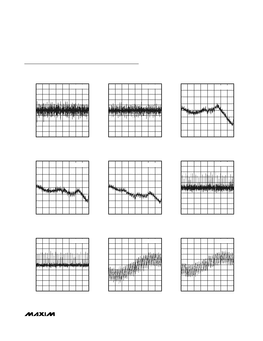
5
-1.0
-0.6
-0.8
-0.2
-0.4
0.2
0
0.4
0.8
0.6
1.0
0
256 384
128
512 640 768 896 1024
DNL vs. CODE (MAX5483)
MAX5481 toc01
CODE
DNL (LSB)
V
DD
= 2.7V
-1.0
-0.6
-0.8
-0.2
-0.4
0.2
0
0.4
0.8
0.6
1.0
0
256 384
128
512 640 768 896 1024
DNL vs. CODE (MAX5483)
MAX5481 toc02
CODE
DNL (LSB)
V
DD
= 5V
-2.0
-1.0
-1.5
0
-0.5
0.5
1.0
1.5
2.0
INL vs. CODE (MAX5483)
MAX5481 toc03
INL (LSB)
V
DD
= 2.7V
0
256 384
128
512 640 768 896 1024
CODE
-2.0
-1.0
-1.5
0
-0.5
0.5
1.0
1.5
2.0
INL vs. CODE (MAX5483)
MAX5481 toc04
INL (LSB)
V
DD
= 3V
0
256 384
128
512 640 768 896 1024
CODE
-2.0
-1.0
-1.5
0
-0.5
0.5
1.0
1.5
2.0
INL vs. CODE (MAX5483)
MAX5481 toc05
INL (LSB)
V
DD
= 5V
0
256 384
128
512 640 768 896 1024
CODE
-1.0
-0.6
-0.8
-0.2
-0.4
0.2
0
0.4
0.8
0.6
1.0
0
256 384
128
512 640 768 896 1024
DNL vs. CODE (MAX5481)
MAX5481 toc06
CODE
DNL (LSB)
V
DD
= 2.7V
-1.0
-0.6
-0.8
-0.2
-0.4
0.2
0
0.4
0.8
0.6
1.0
0
256 384
128
512 640 768 896 1024
DNL vs. CODE (MAX5481)
MAX5481 toc07
CODE
DNL (LSB)
V
DD
= 5V
-1.0
-0.6
-0.8
-0.2
-0.4
0.2
0
0.4
0.8
0.6
1.0
0
256 384
128
512 640 768 896 1024
INL vs. CODE (MAX5481)
MAX5481 toc08
CODE
INL (LSB)
V
DD
= 2.7V
-1.0
-0.6
-0.8
-0.2
-0.4
0.2
0
0.4
0.8
0.6
1.0
0
256 384
128
512 640 768 896 1024
INL vs. CODE (MAX5481)
MAX5481 toc09
CODE
INL (LSB)
V
DD
= 5V
Typical Operating Characteristics
(V
DD
= 5.0V, V
SS
= 0, T
A
= +25°C, unless otherwise noted.)