Äîêóìåíòàöèÿ è îïèñàíèÿ www.docs.chipfind.ru
General Description
The MAX5477/MAX5478/MAX5479 nonvolatile, dual,
linear-taper, digital potentiometers perform the function
of a mechanical potentiometer, but replace the
mechanics with a simple 2-wire digital interface. Each
device performs the same function as a discrete poten-
tiometer or variable resistor and has 256 tap points.
The devices feature an internal, nonvolatile EEPROM
used to store the wiper position for initialization during
power-up. A write-protect feature prevents accidental
overwrites of the EEPROM. The fast-mode I
2
C-compati-
ble serial interface allows communication at data rates
up to 400kbps, minimizing board space and reducing
interconnection complexity in many applications. Three
address inputs allow a total of eight unique address
combinations.
The MAX5477/MAX5478/MAX5479 provide three nomi-
nal resistance values: 10k
(MAX5477), 50k
(MAX5478), or 100k
(MAX5479). The nominal resistor
temperature coefficient is 35ppm/°C end-to-end and
5ppm/°C ratiometric. The low temperature coefficient
makes the devices ideal for applications requiring a low-
temperature-coefficient variable resistor, such as low-
drift, programmable gain-amplifier circuit configurations.
The MAX5477/MAX5478/MAX5479 are available in 16-
pin 3mm x 3mm x 0.8mm thin QFN and 14-pin 4.4mm x
5mm TSSOP packages. These devices operate over
the extended -40°C to +85°C temperature range.
Applications
Mechanical Potentiometer Replacement
Low-Drift Programmable-Gain Amplifiers
Volume Control
Liquid-Crystal Display (LCD) Contrast Control
Features
Power-On Recall of Wiper Position from
Nonvolatile Memory
EEPROM Write Protection
Tiny 3mm x 3mm x 0.8mm Thin QFN Package
35ppm/°C End-to-End Resistance Temperature
Coefficient
5ppm/°C Ratiometric Temperature Coefficient
Fast 400kbps I
2
C
-Compatible Serial Interface
1µA (max) Static Supply Current
Single-Supply Operation: +2.7V to +5.25V
256 Tap Positions per Potentiometer
±0.5 LSB DNL in Voltage-Divider Mode
±1 LSB INL in Voltage-Divider Mode
MAX5477/MAX5478/MAX5479
Dual, 256-Tap, Nonvolatile, I
2
C-Interface,
Digital Potentiometers
________________________________________________________________ Maxim Integrated Products
1
MAX5477
MAX5478
MAX5479
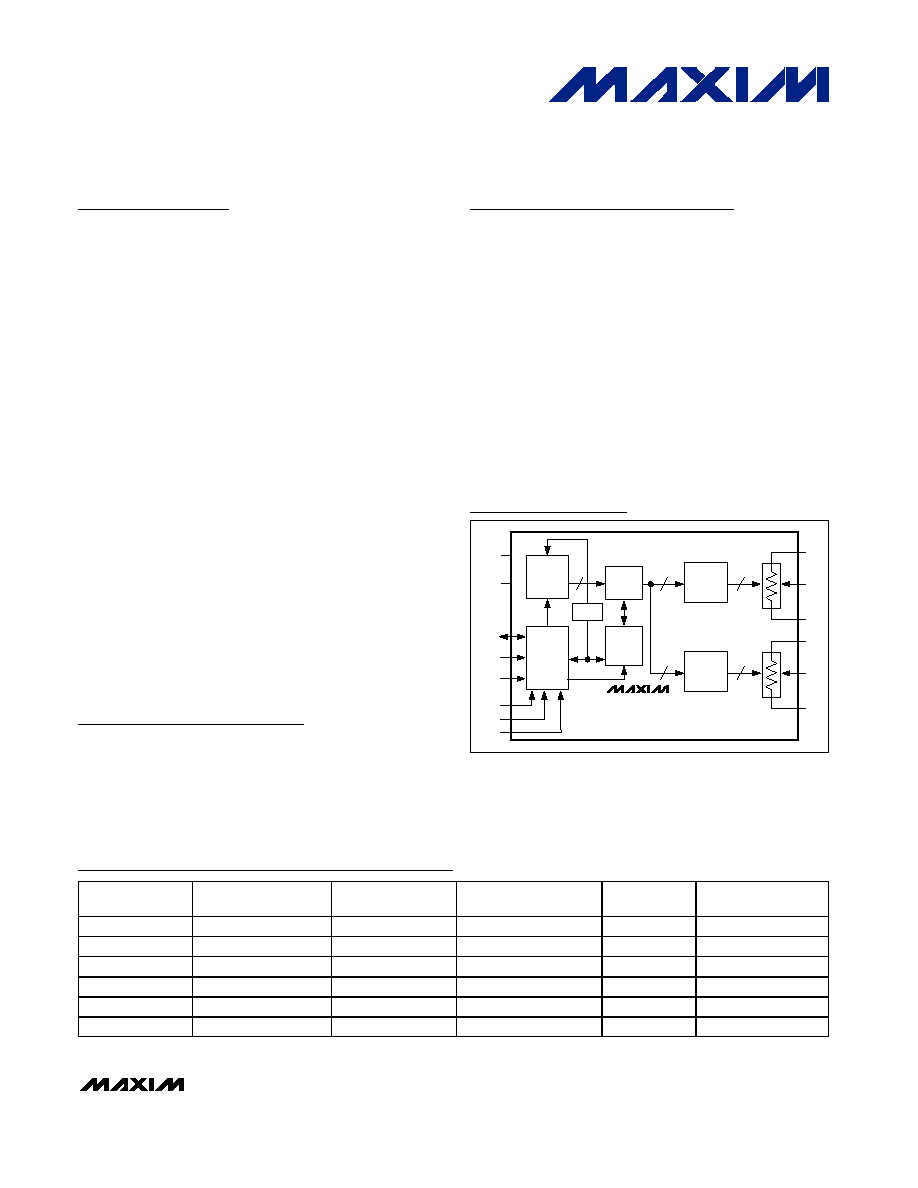
8-BIT
SHIFT
REGISTER
POR
16-BIT
LATCH
16-BIT
NV
MEMORY
SDA
SCL
WP
A0
A1
A2
8
256
POSITION
DECODER
8
8
256
256
POSITION
DECODER
256
HA
WA
LA
HB
WB
LB
V
DD
GND
I
2
C
INTERFACE
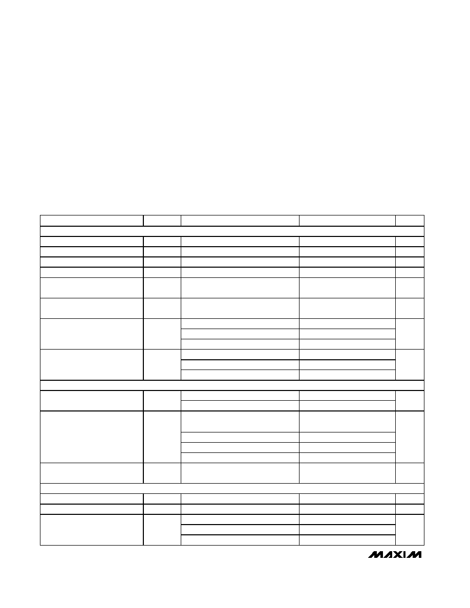
Ordering Information/Selector Guide
Functional Diagram
19-3379; Rev 2; 12/04
For pricing, delivery, and ordering information, please contact Maxim/Dallas Direct! at
1-888-629-4642, or visit Maxim's website at www.maxim-ic.com.
Pin Configurations appear at end of data sheet.
Purchase of I
2
C components from Maxim Integrated
Products, Inc. or one of its sublicensed Associated
Companies, conveys a license under the Philips I
2
C Patent
Rights to use these components in an I
2
C system, provided
that the system conforms to the I
2
C Standard Specification as
defined by Philips.
PART
TEMP RANGE
PIN-PACKAGE
END-TO-END
RESISTANCE (k
)
TOP
MARK
PACKAGE CODE
MAX5477ETE*
-40°C to +85°C
16 Thin QFN
10
ABO
T1633F-3
MAX5477EUD*
-40°C to +85°C
14 TSSOP
10
--
--
MAX5478ETE*
-40°C to +85°C
16 Thin QFN
50
ABP
T1633F-3
MAX5478EUD
-40°C to +85°C
14 TSSOP
50
--
--
MAX5479ETE*
-40°C to +85°C
16 Thin QFN
100
ABQ
T1633F-3
MAX5479EUD
-40°C to +85°C
14 TSSOP
100
--
--
*Future product--contact factory for availability.
MAX5477/MAX5478/MAX5479
Dual, 256-Tap, Nonvolatile, I
2
C-Interface,
Digital Potentiometers
2
_______________________________________________________________________________________
ABSOLUTE MAXIMUM RATINGS
ELECTRICAL CHARACTERISTICS
(V
DD
= +2.7V to +5.25V, H_ = V
DD
, L_ = GND, T
A
= -40°C to +85°C, unless otherwise noted. Typical values are at V
DD
= +5V, T
A
=
+25°C.) (Note 1)
Stresses beyond those listed under "Absolute Maximum Ratings" may cause permanent damage to the device. These are stress ratings only, and functional
operation of the device at these or any other conditions beyond those indicated in the operational sections of the specifications is not implied. Exposure to
absolute maximum rating conditions for extended periods may affect device reliability.
SDA, SCL, V
DD
to GND .........................................-0.3V to +6.0V
All Other Pins to GND.................................-0.3V to (V
DD
+ 0.3V)
Maximum Continuous Current into H_, L_, and W_
MAX5477......................................................................
±5.0mA
MAX5478......................................................................
±1.3mA
MAX5479......................................................................
±0.6mA
Continuous Power Dissipation (T
A
= +70°C)
16-Pin Thin QFN (derate 17.5mW/°C above +70°C) 1399mW
14-Pin TSSOP (derate 9.1mW/°C above +70°C) .........727mW
Operating Temperature Range ...........................-40°C to +85°C
Maximum Junction Temperature .....................................+150°C
Storage Temperature Range .............................-65°C to +150°C
Lead Temperature (soldering, 10s) .................................+300°C
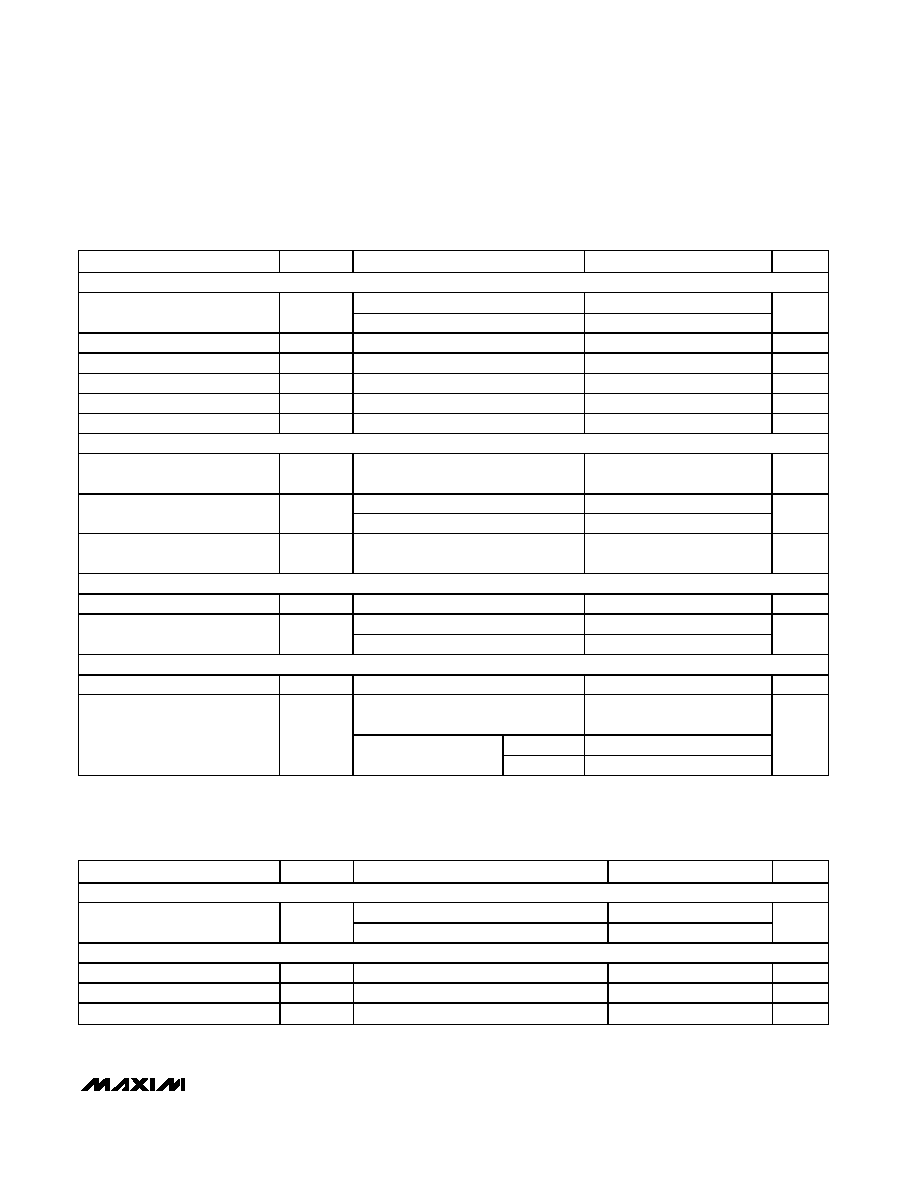
PARAMETER
SYMBOL
CONDITIONS
MIN
TYP
MAX
UNITS
DC PERFORMANCE (VOLTAGE-DIVIDER MODE)
Resolution
256
Taps
Integral Nonlinearity
INL
(Note 2)
±1
LSB
Differential Nonlinearity
DNL
(Note 2)
±0.5
LSB
Dual Code Matching
R0 and R1 set to same code (all codes)
±1
LSB
End-to-End Resistance
Temperature Coefficient
TC
R
35
ppm/°C
Ratiometric Resistance
Temperature Coefficient
5
ppm/°C
MAX5477
-3
MAX5478
-0.6
Full-Scale Error
MAX5479
-0.3
LSB
MAX5477
3
MAX5478
0.6
Zero-Scale Error
MAX5479
0.3
LSB
DC PERFORMANCE (VARIABLE-RESISTOR MODE)
V
DD
= 3V
±3
Integral Nonlinearity (Note 3)
INL
V
DD
= 5V
±1.5
LSB
V
DD
= 3V, MAX5477, guaranteed
monotonic
±1
V
DD
= 3V, MAX5478
±1
V
DD
= 3V, MAX5479
±1
Differential Nonlinearity (Note 3)
DNL
V
DD
= 5V
±1
LSB
Dual Code Matching
R0 and R1 set to same code
(all codes), V
DD
= 3V or 5V
±3
LSB
DC PERFORMANCE (RESISTOR CHARACTERISTICS)
Wiper Resistance
R
W
(Note 4)
325
675
Wiper Capacitance
C
W
10
pF
MAX5477
7.5
10
12.5
MAX5478
37.5
50
62.5
End-to-End Resistance
R
HL
MAX5479
75
100
125
k
MAX5477/MAX5478/MAX5479
Dual, 256-Tap, Nonvolatile, I
2
C-Interface,
Digital Potentiometers
_______________________________________________________________________________________
3
ELECTRICAL CHARACTERISTICS (continued)
(V
DD
= +2.7V to +5.25V, H_ = V
DD
, L_ = GND, T
A
= -40°C to +85°C, unless otherwise noted. Typical values are at V
DD
= +5V, T
A
=
+25°C.) (Note 1)
PARAMETER
SYMBOL
CONDITIONS
MIN
TYP
MAX
UNITS
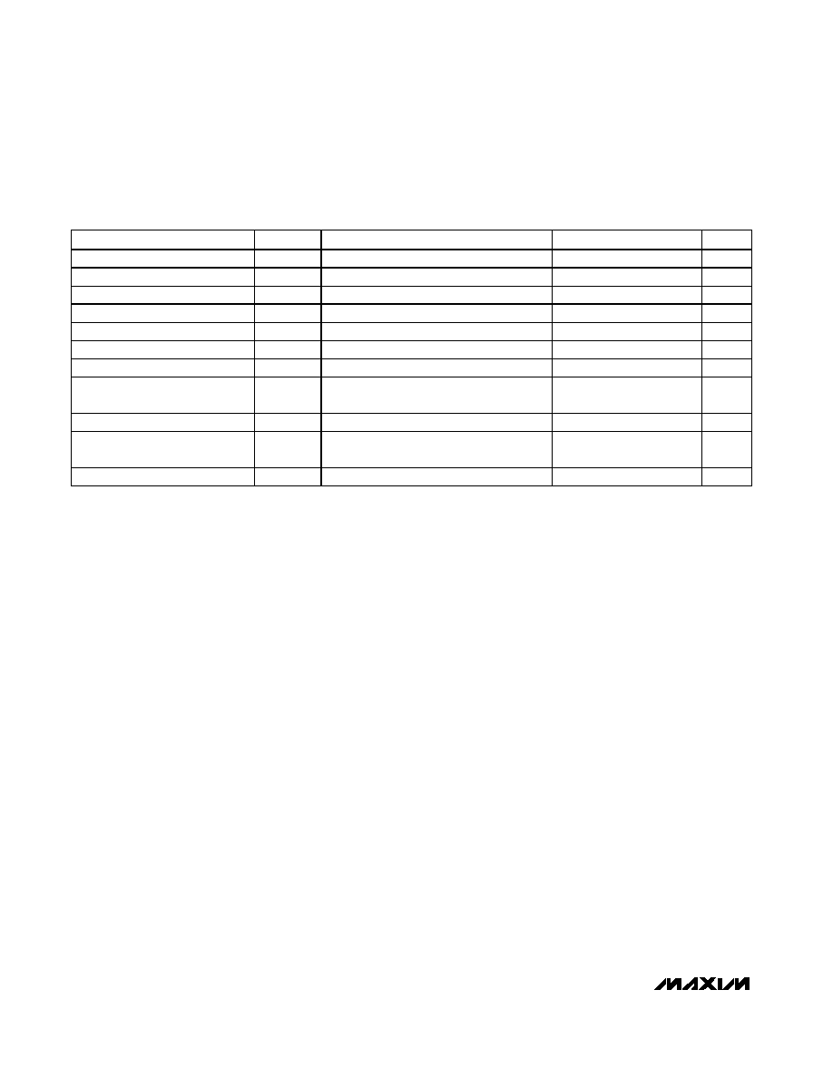
DIGITAL INPUTS
V
DD
= 3.4V to 5.25V
2.4
Input High Voltage (Note 5)
V
IH
V
DD
< 3.4V
0.7 x V
DD
V
Input Low Voltage
V
IL
(Note 5)
0.8
V
Output Low Voltage
V
OL
I
SINK
= 3mA
0.4
V
WP Pullup Resistance
I
WP
255
k
Input Leakage Current
I
LEAK
±1
µA
Input Capacitance
5
pF
DYNAMIC CHARACTERISTICS
Crosstalk
HA = 1kHz (0 to V
DD
), LA = GND,
LB = GND, measure WB
-80
dB
MAX5478
100
3dB Bandwidth (Note 6)
MAX5479
50
kHz
Total Harmonic Distortion Plus
Noise
THD+N
H_ = 1V
RMS
, f = 1kHz, L_ = GND,
measure W_
0.003
%
NONVOLATILE MEMORY RELIABILITY
Data Retention
T
A
= +85°C
50
Years
T
A
= +25°C
200,000
Endurance
T
A
= +85°C
50,000
Stores
POWER SUPPLY
Power-Supply Voltage
V
DD
2.70
5.25
V
Writing to EEPROM, digital inputs at
GND or V
DD
(Note 7)
250
400
WP = GND
15
20.6
Supply Current
I
DD
Normal operation, digital
inputs at GND or V
DD
WP = V
DD
0.5
1
µA
PARAMETER
SYMBOL
CONDITIONS
MIN
TYP
MAX
UNITS
ANALOG SECTION
MAX5478
500
Wiper Settling Time (Note 10)
t
WS
MAX5479
1000
ns
DIGITAL SECTION
SCL Clock Frequency
f
SCL
400
kHz
Setup Time for START Condition
t
SU:STA
0.6
µs
Hold Time for START Condition
t
HD:STA
0.6
µs
TIMING CHARACTERISTICS
(V
DD
= +2.7V to +5.25V, H_ = V
DD
, L_ = GND, T
A
= -40°C to +85°C, unless otherwise noted. Typical values are at V
DD
= +5V,
T
A
= +25°C. See Figure 1.) (Notes 8 and 9)
MAX5477/MAX5478/MAX5479
Dual, 256-Tap, Nonvolatile, I
2
C-Interface,
Digital Potentiometers
4
_______________________________________________________________________________________
Note 1:
All devices are production tested at T
A
= +25°C and are guaranteed by design and characterization for -40°C < T
A
< +85°C.
Note 2:
The DNL and INL are measured with the potentiometer configured as a voltage-divider with H_ = V
DD
and L_ = GND. The
wiper terminal is unloaded and measured with a high-input-impedance voltmeter.
Note 3:
The DNL and INL are measured with the potentiometer configured as a variable resistor. H_ is unconnected and L_ =
GND. For V
DD
= +5V, the wiper is driven with 400µA (MAX5477), 80µA (MAX5478), or 40µA (MAX5479). For V
DD
= +3V,
the wiper is driven with 200µA (MAX5477), 40µA (MAX5478), or 20µA (MAX5479).
Note 4:
The wiper resistance is measured using the source currents given in Note 3.
Note 5:
The devices draw current in excess of the specified supply current when the digital inputs are driven with voltages between
(V
DD
- 0.5V) and (GND + 0.5V). See Supply Current vs. Digital Input Voltage in the Typical Operating Characteristics.
Note 6:
Wiper at midscale with a 10pF load (DC measurement). L_ = GND, an AC source is applied to H_, and the W_ output is
measured. A 3dB bandwidth occurs when the AC W_/H_ value is 3dB lower than the DC W_/H_ value.
Note 7:
The programming current exists only during power-up and EEPROM writes.
Note 8:
The SCL clock period includes rise and fall times (t
R
= t
F
). All digital input signals are specified with t
R
= t
F
= 2ns and
timed from a voltage level of (V
IL
+ V
IH
) / 2.
Note 9:
Digital timing is guaranteed by design and characterization, and is not production tested.
Note 10: This is measured from the STOP pulse to the time it takes the output to reach 50% of the output step size (divider mode). It
is measured with a maximum external capacitive load of 10pF.
Note 11: An appropriate bus pullup resistance must be selected depending on board capacitance. Refer to the I
2
C-bus specifica-
tion document linked to this web address: www.semiconductors.philips.com/acrobat/literature/9398/39340011.pdf
Note 12: The idle time begins from the initiation of the STOP pulse.
PARAMETER
SYMBOL
CONDITIONS
MIN
TYP
MAX
UNITS
SCL High Time
t
HIGH
0.6
µs
SCL Low Time
t
LOW
1.3
µs
Data Setup Time
t
SU:DAT
100
ns
Data Hold Time
t
HD:DAT
0
0.9
µs
SDA, SCL Rise Time
t
R
300
ns
SDA, SCL Fall Time
t
F
300
ns
Setup Time for STOP Condition
t
SU:STO
0.6
µs
Bus Free Time Between STOP
and START Condition
t
BUF
Minimum power-up rate = 0.2V/µs
1.3
µs
Pulse Width of Spike Suppressed
t
SP
50
ns
Capacitive Load for Each Bus
Line
C
B
(Note 11)
400
pF
Write NV Register Busy Time
(Note 12)
12
ms
TIMING CHARACTERISTICS (continued)
(V
DD
= +2.7V to +5.25V, H_ = V
DD
, L_ = GND, T
A
= -40°C to +85°C, unless otherwise noted. Typical values are at V
DD
= +5V,
T
A
= +25°C. See Figure 1.) (Notes 8 and 9)
MAX5477/MAX5478/MAX5479
Dual, 256-Tap, Nonvolatile, I
2
C-Interface,
Digital Potentiometers
_______________________________________________________________________________________
5
SUPPLY CURRENT
vs. TEMPERATURE
MAX5477/78/79 toc01
TEMPERATURE (
°C)
SUPPLY CURRENT (
µ
A)
60
35
10
-15
0.1
0.2
0.3
0.4
0.5
0.6
0.7
0.8
0.9
1.0
0
-40
85
V
DD
= 5V
V
DD
= 3V
0
100
50
200
150
300
250
350
450
400
500
0
64
96
32
128 160 192 224 256
WIPER RESISTANCE
vs. INPUT CODE
MAX5477/78/79 toc02
INPUT CODE
WIPER RESISTANCE (
)
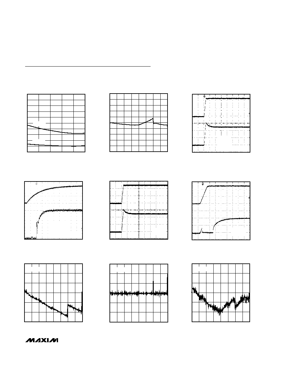
TAP-TO-TAP SWITCHING TRANSIENT
MAX5477/78/79 toc03
1
µs/div
SDA
2V/div
W_
20mV/div
MAX5478
C
L
= 10pF
H_ = V
DD
FROM TAP 00 TO TAP 04
TAP-TO-TAP SWITCHING TRANSIENT
MAX5477/78/79 toc04
400ns/div
SDA
2V/div
W_
20mV/div
MAX5479
C
W_
= 10pF
H_ = V
DD
FROM TAP 00 TO TAP 04
WIPER TRANSIENT AT POWER-ON
MAX5477/78/79 toc05
4
µs/div
V
DD
2V/div
W_
1V/div
MAX5478
TAP = 128
WIPER TRANSIENT AT POWER-ON
MAX5477/78/79 toc06
2
µs/div
V
DD
2V/div
W_
1V/div
MAX5479
TAP = 128
-0.3
-0.2
-0.1
0
0.1
0.2
0.3
0
64
32
96
128 160 192 224 256
INTEGRAL NONLINEARITY
vs. CODE (VDM MODE)
MAX5477/78/79 toc07
CODE
INL (LSB)
MAX5478
-0.3
-0.2
-0.1
0
0.1
0.2
0.3
0
64
32
96
128 160 192 224 256
DIFFERENTIAL NONLINEARITY
vs. CODE (VDM MODE)
MAX5477/78/79 toc08
CODE
DNL (LSB)
MAX5478
-0.3
-0.2
-0.1
0
0.1
0.2
0.3
0
64
32
96
128 160 192 224 256
INTEGRAL NONLINEARITY
vs. CODE (VRM MODE)
MAX5477/78/79 toc09
CODE
INL (LSB)
MAX5478
Typical Operating Characteristics
(V
DD
= +5V, H_ = V
DD
, L_ = GND, T
A
= +25°C, unless otherwise noted.)