
General Description
The MAX5471/MAX5472/MAX5474/MAX5475 linear-
taper digital potentiometers function as mechanical
potentiometers, but replace the mechanics with a sim-
ple 3-wire up/down digital interface. These digital
potentiometers feature nonvolatile memory (EEPROM)
to return the wiper to its previously stored position upon
power-up.
The MAX5471/MAX5472 are 2-terminal, variable resistors
in 6-pin SOT23 packages. The MAX5474/MAX5475 are
3-terminal potentiometers in 8-pin SOT23 packages.
The MAX5471/MAX5474 have an end-to-end resistance
of 50k
, and the MAX5472/MAX5475 have an end-
to-end resistance of 100k
. All of these devices have
32 wiper positions, a low ratiometric temperature coeffi-
cient (5ppm/°C), and all operate from a single +2.7V to
+5.25V supply. Each device is guaranteed over the
extended -40
°C to +85°C temperature range.
Applications
Mechanical Potentiometer Replacement
Liquid-Crystal-Display (LCD) Screen Adjustment
Audio Volume Control
Programmable Filters
Features
o Wiper Position Stored in Nonvolatile Memory and
Recalled Upon Power-Up
o Tiny SOT23 Package
o 35ppm/°C End-to-End Resistance Temperature
Coefficient
o 5ppm/°C Ratiometric Temperature Coefficient
o 32 Tap Positions
o Voltage-Divider or Variable-Resistor
Potentiometer Configuration
o 50k and 100k End-to-End Resistance Values
o 1µA (max) Static Supply Current
o 2.7V to 5.25V Single-Supply Operation
o 200,000 Wiper Store Cycles
o 50-Year Wiper Data Retention
MAX5471/MAX5472/MAX5474/MAX5475
32-Tap, Nonvolatile, Linear-Taper Digital
Potentiometers in SOT23
________________________________________________________________ Maxim Integrated Products
1
Ordering Information
19-3067; Rev 0; 10/03
For pricing, delivery, and ordering information, please contact Maxim/Dallas Direct! at
1-888-629-4642, or visit Maxim's website at www.maxim-ic.com.
PART
TEMP RANGE
PIN-PACKAGE
MAX5471EZT-T
-40
°C to +85°C
6 Thin SOT23-6
MAX5472EZT-T
-40
°C to +85°C
6 Thin SOT23-6
MAX5474EKA-T
-40
°C to +85°C
8 SOT23-8
MAX5475EKA-T
-40
°C to +85°C
8 SOT23-8
TOP VIEW
L
GND
H
INC
W
1
GND
SOT23-6
SOT23-8
2
3
6
5
4
CS
U/D
U/D
MAX5471
MAX5472
1
V
DD
V
DD
H
2
3
8
7
6
CS
MAX5474
MAX5475
4
5
INC
Pin Configurations
PART
END-TO-END
RESISTANCE (k
)
TOP MARK
MAX5471EZT
50
ABQN
MAX5472EZT
100
ABQM
MAX5474EKA
50
AEIZ
MAX5475EKA
100
AEIY
Selector Guide
MAX5471/MAX5472/MAX5474/MAX5475
32-Tap, Nonvolatile, Linear-Taper Digital
Potentiometers in SOT23
2
_______________________________________________________________________________________
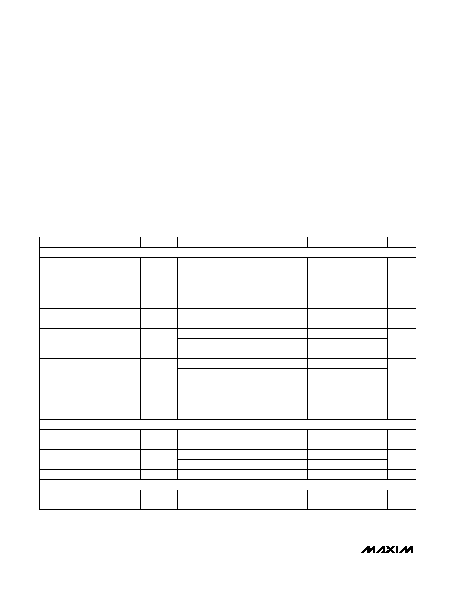
ABSOLUTE MAXIMUM RATINGS
ELECTRICAL CHARACTERISTICS
(V
DD
= +2.7V to +5.25V, V
H
= V
DD
, V
L
= GND, T
A
= -40
°C to +85°C, unless otherwise noted. Typical values are at V
DD
= +5.0V, T
A
= +25
°C, unless otherwise noted.) (Note 1)
Stresses beyond those listed under "Absolute Maximum Ratings" may cause permanent damage to the device. These are stress ratings only, and functional
operation of the device at these or any other conditions beyond those indicated in the operational sections of the specifications is not implied. Exposure to
absolute maximum rating conditions for extended periods may affect device reliability.
V
DD
to GND ...........................................................-0.3V to +6.0V
All Other
Pins to GND .........-0.3V to the lower of (V
DD
+ 0.3V) or +6.0V
Maximum Continuous Current into H, L, and W
MAX5471/MAX5474 .....................................................
±1.3mA
MAX5472/MAX5475 .....................................................
±0.6mA
Continuous Power Dissipation (T
A
= +70
°C)
6-Pin SOT23 (derate 9.1mW/
°C above +70°C)............727mW
8-Pin SOT23 (derate 8.9mW/
°C above +70°C)............714mW
Operating Temperature Range ...........................-40
°C to +85°C
Junction Temperature ......................................................+150
°C
Storage Temperature Range .............................-60
°C to +150°C
Lead Temperature (soldering, 10s) .................................+300
°C
PARAMETER
SYMBOL
CONDITIONS
MIN
TYP
MAX
UNITS
DC PERFORMANCE
Resolution
N
32
Tap
MAX5471/MAX5474
37.5
50
62.5
End-to-End Resistance
MAX5472/MAX5475
75
100
125
k
End-to-End Resistance
Temperature Coefficient
TC
R
35
ppm/
°C
Ratiometric Resistance
Temperature Coefficient
5
ppm/
°C
Variable-resistor mode (Note 2)
±0.5
±1.0
Integral Nonlinearity
INL
Voltage-divider mode (MAX5474/MAX5475)
(Note 3)
±0.1
±0.5
LSB
Variable-resistor mode (Note 2)
±0.5
±1.0
Differential Nonlinearity
DNL
Voltage-divider mode (MAX5474/MAX5475)
(Note 3)
±0.1
±0.5
LSB
Full-Scale Error
MAX5474/MAX5475
-0.5
LSB
Zero-Scale Error
MAX5474/MAX5475
+0.5
LSB
Wiper Resistance
R
W
MAX5474/MAX5475 (Note 4)
600
1200
DIGITAL INPUTS (CS, U/D, INC) (Note 5)
V
DD
< 3.6V
0.7 x V
DD
Input High Voltage
V
IH
V
DD
3.6V
2.4
V
V
DD
< 3.6V
0.3 x V
DD
Input Low Voltage
V
IL
V
DD
3.6V
0.8
V
Input Current
I
IN
±0.1
±1
µA
DYNAMIC CHARACTERISTICS
MAX5471/MAX5474
400
Wiper -3dB Bandwidth (Note 6)
MAX5472/MAX5475
200
kHz

MAX5471/MAX5472/MAX5474/MAX5475
32-Tap, Nonvolatile, Linear-Taper Digital
Potentiometers in SOT23
_______________________________________________________________________________________
3
Note 1: All devices are production tested at T
A
= +25°C and are guaranteed by design and characterization for -40°C < T
A
< +85°C.
Note 2: The DNL and INL are measured with the potentiometer configured as a variable resistor. For the 3-terminal potentiometers
(MAX5474/MAX5475), H is unconnected and L = GND. At V
DD
= 5.25V, W is driven with a source current of 80µA for the
50k
configuration, and 40µA for the 100k configuration. At V
DD
= 2.7V, the wiper terminal is driven with a source current
of 40µA for the 50k
configuration, and 20µA for the 100k configuration.
Note 3: The DNL and INL are measured with the potentiometer configured as a voltage-divider with H = V
DD
and L = GND
(MAX5474/MAX5475 only). The wiper terminal is unloaded.
Note 4: The wiper resistance is the worst value measured by injecting the currents given in Note 2 into W with L = GND.
R
W
= (V
W
- V
H
) / I
W
.
Note 5: The device draws higher supply current when digital inputs are driven with voltages between 0.3V x V
DD
and 0.7 x V
DD
.
Drive the digital inputs as close as possible to V
DD
or GND. (See the Typical Operating Characteristics for the Supply
Current vs. Digital Input Voltage graph.)
Note 6: Wiper at midscale with a 10pF load.
Note 7: Digital timing is guaranteed by design and characterization, and is not production tested.
Note 8: Wiper settling time is the worst-case 0% to 50% rise time measured between consecutive wiper positions. H = V
DD
, L =
GND, and the wiper terminal is unloaded and measured with a 10pF oscilloscope probe (see the Typical Operating
Characteristics for the Tap-to-Tap Switching Transient).
Note 9: Digital inputs CS, U/D, and INC are connected to GND or V
DD
. See the Typical Operating Characteristics for the Static
Supply Current vs. Temperature graph.
ELECTRICAL CHARACTERISTICS (continued)
(V
DD
= +2.7V to +5.25V, V
H
= V
DD
, V
L
= GND, T
A
= -40
°C to +85°C, unless otherwise noted. Typical values are at V
DD
= +5.0V, T
A
= +25
°C, unless otherwise noted.) (Note 1)
PARAMETER
SYMBOL
CONDITIONS
MIN
TYP
MAX
UNITS
TIMING CHARACTERISTICS (Figure 1, Note 7)
CS to INC Setup
t
CI
50
ns
INC High to U/D Change
t
ID
0
ns
U/D to INC Setup
t
DI
100
ns
INC Low Period
t
IL
50
ns
INC High Period
t
IH
50
ns
INC Cycle Time
t
CYC
100
ns
INC Inactive to CS Inactive
t
IC
100
ns
INC Active to CS Inactive
t
IK
100
ns
CS Deselect Time (Store)
t
CPH
100
ns
Wiper Settling Time
t
IW
(Note 8)
1
µs
Power-Up to Wiper Stable
t
PU
1
µs
Wiper Store Cycle
t
WSC
12
ms
NONVOLATILE MEMORY RELIABILITY
Data Retention
T
A
= +85°C
50
Year
Endurance
T
A
= +85°C
200,000
Store
POWER SUPPLY
Supply Voltage
V
DD
2.70
5.25
V
Supply Current
I
DD
Write to memory
400
µA
Static Supply Current
I
SD
T
A
= +25°C (Note 9)
0.35
1
µA
MAX5471/MAX5472/MAX5474/MAX5475
32-Tap, Nonvolatile, Linear-Taper Digital
Potentiometers in SOT23
4
_______________________________________________________________________________________
Typical Operating Characteristics
(V
DD
= 5.0V, T
A
= +25
°C, unless otherwise noted.)
SUPPLY CURRENT vs. SUPPLY VOLTAGE
MAX5471 toc01
SUPPLY VOLTAGE (V)
SUPPLY CURRENT (
µ
A)
5.1
4.7
4.3
3.9
3.5
3.1
0.1
0.2
0.3
0.4
0.5
0
2.7
5.5
DIGITAL INPUTS = GND OR V
DD
STATIC SUPPLY CURRENT
vs. TEMPERATURE
MAX5471 toc02
TEMPERATURE (
°C)
SUPPLY CURRENT (
µ
A)
60
35
10
-15
0.1
0.2
0.3
0.4
0.5
0
-40
85
DIGITAL INPUTS = GND OR V
DD
V
DD
= 5.0V
V
DD
= 3.0V
SUPPLY CURRENT
vs. DIGITAL INPUT VOLTAGE
MAX5471 toc03
DIGITAL INPUT VOLTAGE (V)
SUPPLY CURRENT (
µ
A)
4
3
2
1
1
10
100
1000
10,000
0.1
0
5
V
DD
= 5.0V
V
DD
= 3.0V
WIPER RESISTANCE
vs. TAP POSITION (MAX5474)
MAX5471 toc04
TAP POSITION
WIPER RESISTANCE (
)
25
20
5
10
15
250
300
350
400
450
500
550
600
200
0
30
V
DD
= 3.0V
V
DD
= 5.0V
WIPER RESISTANCE
vs. TAP POSITION (MAX5475)
MAX5471 toc05
TAP POSITION
WIPER RESISTANCE (
)
25
20
5
10
15
250
300
350
400
450
500
550
600
200
0
30
V
DD
= 3.0V
V
DD
= 5.0V
END-TO-END RESISTANCE % CHANGE
vs. TEMPERATURE
MAX5471 toc06
TEMPERATURE (
°C)
END-TO-END RESISTANCE % CHANGE
60
35
-15
10
-0.15
-0.10
-0.05
0
0.05
0.10
0.15
0.20
-0.20
-40
85
100k
100k
50k
50k
W-TO-L RESISTANCE
vs. TAP POSITION
MAX5471 toc07
TAP POSITION
W-TO-L RESISTANCE (k
)
25
20
15
10
5
20
40
60
80
100
0
0
30
MAX5475
MAX5474
H-TO-GND RESISTANCE
vs. TAP POSITION
MAX5471 toc08
TAP POSITION
H-TO-GND RESISTANCE (k
)
25
20
15
10
5
20
40
60
80
100
0
0
30
MAX5472
MAX5471
TAP-TO-TAP SWITCHING TRANSIENT
MAX5471 toc09
400ns/div
INC
5V/div
W
100mV/div
C
L
= 10pF
V
H
= V
DD
TAP 16 TO TAP 15
MAX5474
MAX5475
MAX5471/MAX5472/MAX5474/MAX5475
32-Tap, Nonvolatile, Linear-Taper Digital
Potentiometers in SOT23
_______________________________________________________________________________________
5
WIPER TRANSIENT AT POWER-ON
(MAX5475)
MAX5471 toc11
1.0
µs/div
V
DD
5V/div
W
1V/div
C
L
= 10pF
TAP 16
V
H
= V
DD
WIPER RESPONSE vs. FREQUENCY
MAX5471toc12
FREQUENCY (kHz)
WIPER RESPONSE (dB)
100
10
-15
-12
-9
-6
-3
0
-18
1
1000
TAP = 16
C
L
= 10pF
MAX5474
MAX5475
RESISTANCE DNL vs. TAP POSITION
(MAX5471)
MAX5471 toc13
TAP POSITION
RESISTANCE DNL
25
20
15
10
5
-0.2
-0.1
0
0.1
0.2
0.3
-0.3
0
30
VARIABLE-RESISTOR MODE
RESISTANCE INL vs. TAP POSITION
(MAX5471)
MAX5471 toc14
TAP POSITION
RESISTANCE INL
25
20
15
10
5
0
0.1
0.2
0.3
0.4
0.5
-0.1
0
30
VARIABLE-RESISTOR MODE
RESISTANCE DNL vs. TAP POSITION
(MAX5472)
MAX5471 toc15
TAP POSITION
RESISTANCE DNL
25
20
15
10
5
-0.2
-0.1
0
0.1
0.2
0.3
-0.3
0
30
VARIABLE-RESISTOR MODE
RESISTANCE INL vs. TAP POSITION
(MAX5472)
MAX5471 toc16
TAP POSITION
RESISTANCE INL
25
20
15
10
5
0
0.1
0.2
0.3
0.4
0.5
-0.1
0
30
VARIABLE-RESISTOR MODE
RESISTANCE DNL vs. TAP POSITION
(MAX5474)
MAX5471 toc17
TAP POSITION
RESISTANCE DNL
25
20
15
10
5
-0.03
-0.02
-0.01
0
0.01
0.02
0.03
0.04
-0.04
0
30
VOLTAGE-DIVIDER MODE
RESISTANCE INL vs. TAP POSITION
(MAX5474)
MAX5471 toc18
TAP POSITION
RESISTANCE INL
25
20
15
10
5
-0.03
-0.02
-0.01
0
0.01
0.02
0.03
0.04
-0.04
0
30
VOLTAGE-DIVIDER MODE
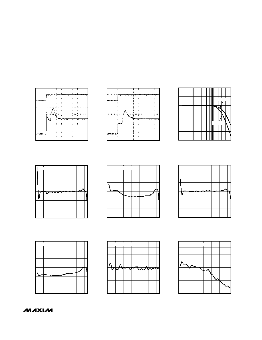
Typical Operating Characteristics (continued)
(V
DD
= 5.0V, T
A
= +25
°C, unless otherwise noted.)
WIPER TRANSIENT AT POWER-ON
(MAX5474)
MAX5471 toc10
1.0
µs/div
V
DD
5V/div
W
1V/div
C
L
= 10pF
TAP 16
V
H
= V
DD