
General Description
The MAX5432MAX5435 nonvolatile, linear-taper, digi-
tal potentiometers perform the function of a mechanical
potentiometer, but replace the mechanics with a simple
2-wire serial interface. Each device performs the same
function as a discrete potentiometer or a variable resis-
tor and has 32 tap points.
The MAX5432MAX5435 feature an internal, nonvolatile,
electrically erasable programmable read-only memory
(EEPROM) that returns the wiper to its previously stored
position at power-up. The fast-mode I
2
C
-compatible
serial interface allows communication at data rates up to
400kbps, minimizing board space and reducing inter-
connection complexity. Each device is available with
one of four factory-preset I
2
C addresses (see the
Selector Guide).
Use the MAX5432MAX5435 in applications requiring
digitally controlled resistors. Two resistance values are
available (50k
and 100k) in a voltage-divider or vari-
able resistor configuration. The nominal resistor temper-
ature coefficient is 35ppm/°C end-to-end, and only
5ppm/°C ratiometric, making the devices ideal for
applications requiring a low-temperature-coefficient
variable resistor such as low-drift, programmable-gain
amplifier circuit configurations.
The MAX5432/MAX5433 are available in a 3mm x 3mm 8-
pin TDFN package and the MAX5434/MAX5435 are avail-
able in a 6-pin thin SOT23 package. The MAX5432
MAX5435 are specified over the extended (-40°C to
+85°C) temperature range.
Applications
Mechanical Potentiometer Replacement
Low-Drift Programmable-Gain Amplifiers
Volume Control
Liquid-Crystal Display (LCD) Screen Adjustment
Features
Tiny 3mm x 3mm 8-Pin TDFN and 6-Pin Thin
SOT23 Packages
Power-On Recall of Wiper Position from
Nonvolatile Memory
35ppm/°C End-to-End Resistance Temperature
Coefficient
5ppm/°C Ratiometric Temperature Coefficient
50k/100k Resistor Values
Fast 400kbps I
2
C-Compatible Serial Interface
500nA (typ) Static Supply Current
+2.7V to +5.25V Single-Supply Operation
32 Tap Positions
±0.15 LSB INL (typ), ±0.15 LSB DNL (typ)
MAX5432MAX5435
32-Tap, Nonvolatile, I
2
C, Linear, Digital
Potentiometers
________________________________________________________________ Maxim Integrated Products
1
Ordering Information
19-3511; Rev 1; 12/04
For pricing, delivery, and ordering information, please contact Maxim/Dallas Direct! at
1-888-629-4642, or visit Maxim's website at www.maxim-ic.com.
PART
TEMP RANGE
PIN-PACKAGE
MAX5432LETA
-40
°C to +85°C
8 TDFN-EP**
MAX5432META*
-40
°C to +85°C
8 TDFN-EP**
MAX5433LETA
-40
°C to +85°C
8 TDFN-EP**
MAX5433META*
-40
°C to +85°C
8 TDFN-EP**
MAX5434LEZT-T
-40
°C to +85°C
6 Thin SOT23-6
MAX5434MEZT-T*
-40
°C to +85°C
6 Thin SOT23-6
MAX5434NEZT-T*
-40
°C to +85°C
6 Thin SOT23-6
MAX5434PEZT-T*
-40
°C to +85°C
6 Thin SOT23-6
MAX5435LEZT-T
-40
°C to +85°C
6 Thin SOT23-6
MAX5435MEZT-T*
-40
°C to +85°C
6 Thin SOT23-6
MAX5435NEZT-T*
-40
°C to +85°C
6 Thin SOT23-6
MAX5435PEZT-T*
-40
°C to +85°C
6 Thin SOT23-6
Purchase of I
2
C components from Maxim Integrated Products,
Inc., or one of its sublicensed Associated Companies, conveys
a license under the Philips I
2
C Patent Rights to use these com-
ponents in an I
2
C system, provided that the system conforms
to the I
2
C Standard Specification as defined by Philips.
Selector Guide appears at end of data sheet.
*Future product--contact factory for availability.
**EP = Exposed pad.
TDFN
TOP VIEW
GND
SDA
SCL
1
6
L
5
W
V
DD
SOT23
2
3
4
MAX5434
MAX5435
A0
V
DD
SCL
1
2
8
7
W
L
SDA
GND
H
3
4
6
5
MAX5432
MAX5433
Pin Configurations
MAX5432MAX5435
32-Tap, Nonvolatile, I
2
C, Linear, Digital
Potentiometers
2
_______________________________________________________________________________________
ABSOLUTE MAXIMUM RATINGS
Stresses beyond those listed under "Absolute Maximum Ratings" may cause permanent damage to the device. These are stress ratings only, and functional
operation of the device at these or any other conditions beyond those indicated in the operational sections of the specifications is not implied. Exposure to
absolute maximum rating conditions for extended periods may affect device reliability.
V
DD
to GND ...........................................................-0.3V to +6.0V
SDA, SCL to GND..................................................-0.3V to +6.0V
A0, H, L, and W to GND .............................-0.3V to (V
DD
+ 0.3V)
Maximum Continuous Current into H, L, and W
MAX5432/MAX5434.....................................................±1.3mA
MAX5433/MAX5435.....................................................±0.6mA
Input/Output Latchup Immunity........................................±50mA
Continuous Power Dissipation (T
A
= +70°C)
6-Pin Thin SOT23 (derate 9.1mW/°C above +70°C) ....727mW
8-Pin TDFN (derate 18.2mW/°C above +70°C) ......1454.5mW
Operating Temperature Range ...........................-40°C to +85°C
Junction Temperature ......................................................+150°C
Storage Temperature Range .............................-60°C to +150°C
Lead Temperature (soldering, 10s) .................................+300°C
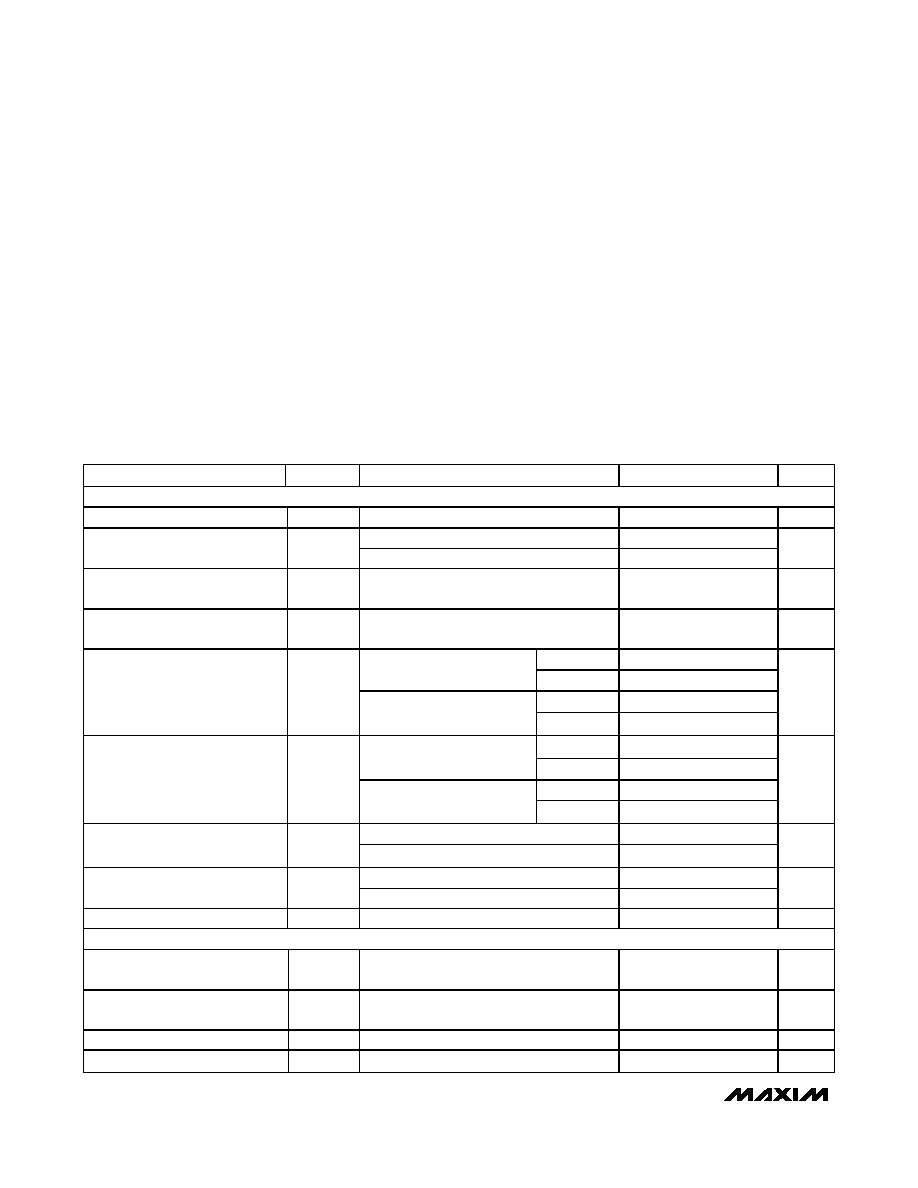
ELECTRICAL CHARACTERISTICS
(V
DD
= +2.7V to +5.25V, V
H
= V
DD
, V
L
= GND, T
A
= -40°C to +85°C, unless otherwise noted. Typical values are at V
DD
= +5V, T
A
=
+25°C.) (Note 1)
PARAMETER
SYMBOL
CONDITIONS
MIN
TYP
MAX
UNITS
DC PERFORMANCE
Resolution
32
Taps
MAX5432/MAX5434
37.5
50
62.5
End-to-End Resistance
R
H-L
MAX5433/MAX5435
75
100
125
k
End-to-End Resistance
Temperature Coefficient
TC
R
35
ppm/°C
Ratiometric Resistance
Temperature Coefficient
5
ppm/°C
V
DD
= 5V
±0.15
±0.5
Variable resistor (Note 2)
V
DD
= 3V
±0.15
±0.5
V
DD
= 5V
±0.15
±0.5
Integral Nonlinearity
INL
Voltage-divider,
MAX5432/MAX5433 (Note 3)
V
DD
= 3V
±0.15
±0.5
LSB
V
DD
= 5V
±0.15
±0.5
Variable resistor (Note 2)
V
DD
= 3V
±0.15
±0.5
V
DD
= 5V
±0.15
±0.5
Differential Nonlinearity
DNL
Voltage-divider,
MAX5432/MAX5433 (Note 3)
V
DD
= 3V
±0.15
±0.5
LSB
MAX5432, 50k
-0.5
Full-Scale Error (Note 4)
MAX5433, 100k
-0.5
LSB
MAX5432, 50k
+0.5
Zero-Scale Error (Note 5)
MAX5433, 100k
+0.5
LSB
Wiper Resistance
R
W
MAX5432/MAX5433 (Note 6)
610
1200
DIGITAL INPUTS
Input High Voltage
V
IH
(Note 7)
0.7 x
V
DD
V
Input Low Voltage
V
IL
(Note 7)
0.3 x
V
DD
V
Input Leakage Current
I
LEAK
±1
µA
Input Capacitance
5
pF

MAX5432MAX5435
32-Tap, Nonvolatile, I
2
C, Linear, Digital
Potentiometers
_______________________________________________________________________________________
3
ELECTRICAL CHARACTERISTICS (continued)
(V
DD
= +2.7V to +5.25V, V
H
= V
DD
, V
L
= GND, T
A
= -40°C to +85°C, unless otherwise noted. Typical values are at V
DD
= +5V, T
A
=
+25°C.) (Note 1)
PARAMETER
SYMBOL
CONDITIONS
MIN
TYP
MAX
UNITS
DYNAMIC CHARACTERISTICS
MAX5432/MAX5434
500
-3dB Bandwidth (Note 8)
MAX5433/MAX5435
250
kHz
MAX5432/MAX5434
0.5
Wiper Settling Time (Note 9)
MAX5433/MAX5435
1.0
µs
NONVOLATILE MEMORY RELIABILITY
Data Retention
T
A
= +85°C
50
Years
T
A
= +25°C
200,000
Endurance
T
A
= +85°C
50,000
Stores
POWER SUPPLY
Power-Supply Voltage
V
DD
2.70
5.25
V
Standby Current
I
DD
Digital inputs = V
DD
or GND, T
A
= +25°C
0.5
2
µA
Programming Current
During nonvolatile write; digital inputs =
V
DD
or GND (Note 10)
200
900
µA
Note 1: All devices are production tested at T
A
= +25°C and are guaranteed by design and characterization for -40°C < T
A
< +85°C.
TIMING CHARACTERISTICS
(V
DD
= +2.7V to +5.25V, V
H
= V
DD
, V
L
= GND, T
A
= -40°C to +85°C, unless otherwise noted. Typical values are at V
DD
= +5V, T
A
=
+25°C.) (Figures 1 and 2) (Note 11)
PARAMETER
SYMBOL
CONDITIONS
MIN
TYP
MAX
UNITS
SCL Clock Frequency
f
SCL
400
kHz
Setup Time for START Condition
t
SU-STA
0.6
µs
Hold Time for START Condition
t
HD-STA
0.6
µs
CLK High Time
t
HIGH
0.6
µs
CLK Low Time
t
LOW
1.3
µs
Data Setup Time
t
SU-DAT
100
ns
Data Hold Time
t
HD-DAT
0
0.9
µs
SDA, SCL Rise Time
t
R
300
ns
SDA, SCL Fall Time
t
F
300
ns
Setup Time for STOP Condition
t
SU-STO
0.6
µs
Bus Free Time Between STOP
and START Condition
t
BUF
1.3
µs
Pulse Width of Spike Suppressed
t
SP
50
ns
Capacitive Load for Each Bus
Line
C
B
(Note 12)
400
pF
Nonvolatile Store Time
Idle time required after a nonvolatile
memory write (Note 13)
12
ms
MAX5432MAX5435
32-Tap, Nonvolatile, I
2
C, Linear, Digital
Potentiometers
4
_______________________________________________________________________________________
TIMING CHARACTERISTICS (continued)
(V
DD
= +2.7V to +5.25V, V
H
= V
DD
, V
L
= GND, T
A
= -40°C to +85°C, unless otherwise noted. Typical values are at V
DD
= +5V, T
A
=
+25°C.) (Figures 1 and 2) (Note 1)
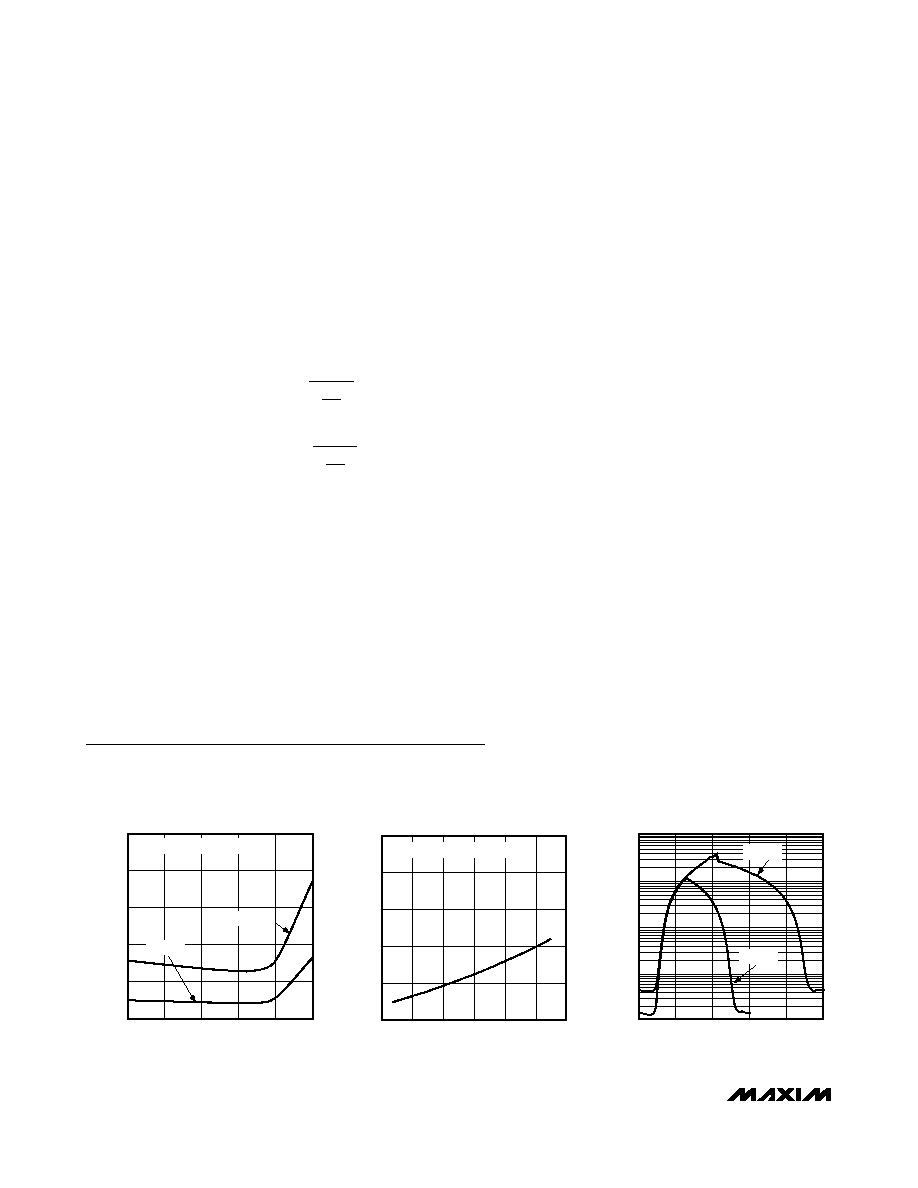
Typical Operating Characteristics
(V
DD
= +5V, T
A
= +25°C, unless otherwise noted.)
0
0.3
0.9
0.6
1.2
1.5
-40
10
-15
35
60
85
STANDBY SUPPLY CURRENT
vs. TEMPERATURE
MAX543235 toc01
TEMPERATURE (
°C)
SUPPLY CURRENT (
µ
A)
DIGITAL INPUTS = GND OR V
DD
V
DD
= 5V
V
DD
= 3V
0
0.2
0.6
0.4
0.8
1.0
2.5
3.5
3.0
4.0
4.5
5.0
5.5
SUPPLY CURRENT
vs. SUPPLY VOLTAGE
MAX543235 toc02
SUPPLY VOLTAGE (V)
SUPPLY CURRENT (
µ
A)
DIGITAL INPUTS = GND OR V
DD
0
2
1
3
5
SUPPLY CURRENT
vs. DIGITAL INPUT VOLTAGE
MAX543235 toc03
DIGITAL INPUT VOLTAGE (V)
SUPPLY CURRENT (
µ
A)
1000
0.1
1
10
100
V
DD
= 5V
V
DD
= 3V
4
V
V
V
W
H
H
-
31
.
V
V
V
W
L
H
-
31
.
Note 2: The DNL and INL are measured with the potentiometer configured as a variable resistor. For the 3-terminal potentiometers
(MAX5432/MAX5433), H is unconnected and L = GND. At V
DD
= 5V, W is driven with a source current of 80µA for the 50k
configuration, and 40µA for the 100k
configuration. At V
DD
= 3V, W is driven with a source current of 40µA for the 50k
configuration, and 20µA for the 100k
configuration.
Note 3: The DNL and INL are measured with the potentiometer configured as a voltage-divider with H = V
DD
and L = GND
(MAX5432/MAX5433 only). The wiper terminal is unloaded and measured with an ideal voltmeter.
Note 4: Full-scale error is defined as
Note 5: Zero-scale error is defined as
Note 6: The wiper resistance is the worst value measured by injecting the currents given in Note 2 into W with L = GND.
R
W
= (V
W
- V
H
) / I
W
.
Note 7: The device draws current in excess of the specified supply current when the digital inputs are driven with voltages between
(V
DD
- 0.5V) and (GND + 0.5V). See the Supply Current vs. Digital Input Voltage graph in the Typical Operating Characteristics.
Note 8: Wiper is at midscale with a 10pF capacitive load. Potentiometer set to midscale, L = GND, an AC source is applied to H,
and the output is measured as 3dB lower than the DC W/H value in dB.
Note 9: This is measured from the STOP pulse to the time it takes the output to reach 50% of the output step size (divider mode). It
is measured with a maximum external capacitive load of 10pF.
Note 10: The programming current exists only during NV writes (12ms typ).
Note 11: Digital timing is guaranteed by design and characterization, and is not production tested.
Note 12: An appropriate bus pullup resistance must be selected depending on board capacitance. Refer to the I
2
C-bus specifica-
tion document linked to this web address: www.semiconductors.philips.com/acrobat/literature/9398/39340011.pdf
Note 13: The idle time begins from the initiation of the stop pulse.
MAX5432MAX5435
32-Tap, Nonvolatile, I
2
C, Linear, Digital
Potentiometers
_______________________________________________________________________________________
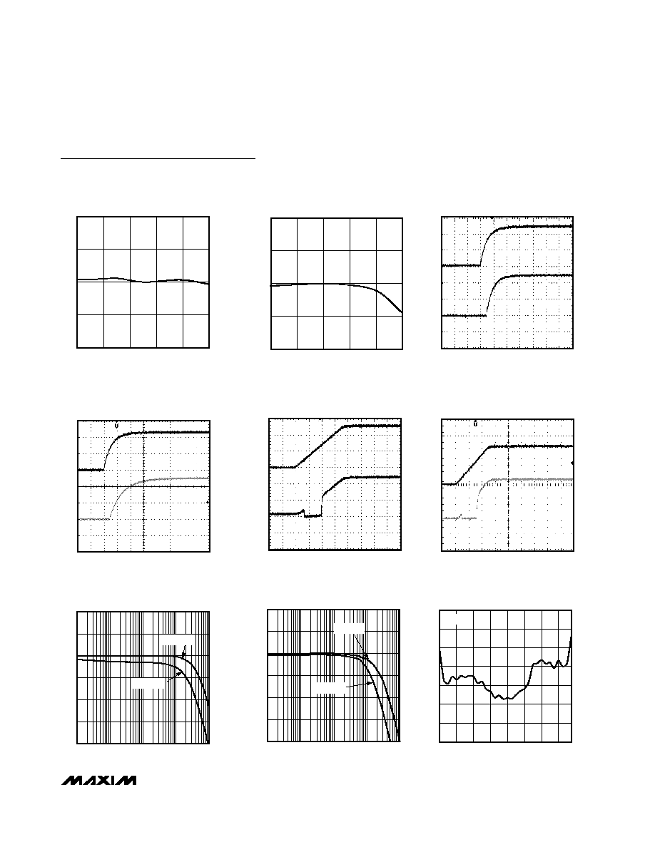
5
1.0
0.5
0
-0.5
-1.0
-40
10
-15
35
60
85
END-TO-END RESISTANCE % CHANGE
vs. TEMPERATURE
MAX543235 toc04
TEMPERATURE (
°C)
END-TO-END RESISTANCE CHANGE ( %)
50k
1.0
0.5
0
-0.5
-1.0
-40
10
-15
35
60
85
END-TO-END RESISTANCE % CHANGE
vs. TEMPERATURE
MAX5432-35 toc05
TEMPERATURE (
°C)
END-TO-END RESISTANCE % CHANGE
100k
1
µs/div
TAP-TO-TAP SWITCHING TRANSIENT
(0 TO MIDSCALE, C
L
= 10pF)
V
W
1V/div
SDA
2V/div
MAX543235 toc06
50k
1
µs/div
TAP-TO-TAP SWITCHING TRANSIENT
(0 TO MIDSCALE, C
L
= 10pF)
V
W
1V/div
SDA
2V/div
MAX543235 toc07
100k
10
µs/div
WIPER TRANSIENT AT POWER-ON
V
W
1V/div
V
DD
2V/div
MAX543235 toc08
50k
10
µs/div
MIDSCALE WIPER TRANSIENT
AT POWER-ON
V
W
1V/div
V
DD
2V/div
MAX543235 toc09
100k
MIDSCALE WIPER RESPONSE
vs. FREQUENCY
(MAX5432)
MAX5432 toc10
FREQUENCY (kHz)
GAIN (dB)
100
10
1
-15
-12
-9
-6
-3
0
-18
0.1
1000
C
W
= 10pF
C
W
= 33pF
-18
-12
-15
-6
-3
-9
0
0.1
1
10
100
1000
MIDSCALE WIPER RESPONSE
vs. FREQUENCY (MAX5433)
MAX543235 toc11
FREQUENCY (kHz)
GAIN (dB)
C
W
= 10pF
C
W
= 33pF
0
100
300
200
500
600
400
700
0
8
12
4
16
20
24
28
31
WIPER RESISTANCE vs. TAP POSITION
(MAX5432)
MAX543235 toc12
TAP POSITION
RESISTANCE (
)
V
DD
= 3V
Typical Operating Characteristics (continued)
(V
DD
= +5V, T
A
= +25°C, unless otherwise noted.)