General Description
The MAX5427/MAX5428/MAX5429 linear-taper digital
potentiometers function as mechanical potentiometers,
but replace the mechanics with a simple 2-wire digital
interface. These digital potentiometers are unique in that
they have an optional one-time programmable feature
that either sets the wiper's power-on reset (POR) posi-
tion to a user-defined value, or the wiper can be set and
the interface disabled to prevent further adjustment.
The MAX5427 has an end-to-end resistance of 100k
,
the MAX5428 a resistance of 50k
, and the MAX5429 a
resistance of 10k
. All these devices have 32 wiper
positions, operate from a single 2.7V to 5.5V supply, and
use less than 1.5µA (max) static supply current.
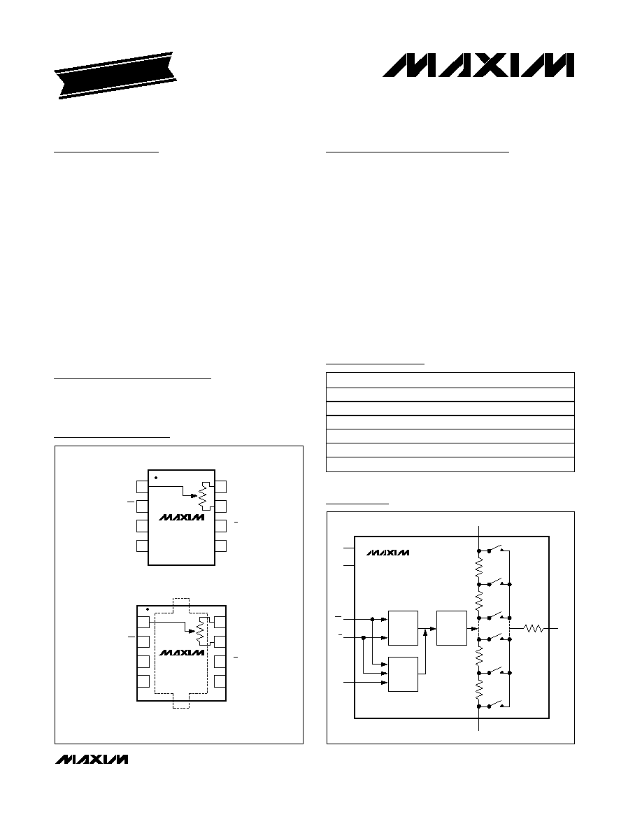
The MAX5427/MAX5428/MAX5429 are available in
8-pin thin QFN and µMAX packages. Each device is
guaranteed over the extended temperature range of
-40°C to +85°C.
Applications
Mechanical Potentiometer Replacement
Products Using One-Time Factory Calibration
Features
o Wiper Position Stored After One-Time Fuse
Programming
o User-Defined Power-On Reset Position
o 35ppm/°C End-to-End Temperature Coefficient
and 5ppm/°C Ratiometric Temperature Coefficient
o 32 Tap Positions
o Tiny 8-Pin Thin QFN and µMAX Packages
o Ultra-Low 1.5µA (max) Static Supply Current
o 2.7V to 5.5V Single-Supply Operation
o Wiper Position Programmed Through Simple
2-Wire Serial Interface
o 10k, 50k, and 100k End-to-End Resistances
MAX5427/MAX5428/MAX5429
One-Time Programmable, Linear-Taper
Digital Potentiometers
________________________________________________________________ Maxim Integrated Products
1
Ordering Information
MAX5427
MAX5428
MAX5429
32-
POSITION
DECODER
UP/DOWN
COUNTER
ONE-TIME
PROGRAM
BLOCK
8
H
S
31
S
32
S
30
S
2
S
3
S
1
R
31
R
30
R
W
R
2
R
1
1
W
7
L
3
4
2
6
5
V
DD
V
PP
GND
CS
U/D
Functional Block Diagram
19-2462; Rev 1; 7/02
For pricing, delivery, and ordering information, please contact Maxim/Dallas Direct! at
1-888-629-4642, or visit Maxim's website at www.maxim-ic.com.
EVALUATION KIT
AVAILABLE
PART
TEMP RANGE
PIN-PACKAGE
R (k
)
MAX5427EUA
-40°C to +85°C
8 µMAX
100
MAX5427ETA
-40°C to +85°C
8 Thin QFN-EP*
100
MAX5428EUA
-40°C to +85°C
8 µMAX
50
MAX5428ETA
-40°C to +85°C
8 Thin QFN-EP*
50
MAX5429EUA
-40°C to +85°C
8 µMAX
10
MAX5429ETA
-40°C to +85°C
8 Thin QFN-EP*
10
V
PP
GND
1
2
8
7
H
L
V
DD
W
µMAX
TOP VIEW
3
4
6
5
MAX5427
MAX5428
MAX5429
CS
U/D
V
PP
GND
*EXPOSED PADDLE. CONNECTED TO GND.
8
7
H
L
V
DD
W
QFN
6
5
MAX5427
MAX5428
MAX5429
CS
U/D
1
2
3
4
*
*
Pin Configurations
*EP = Exposed paddle.

MAX5427/MAX5428/MAX5429
One-Time Programmable, Linear-Taper
Digital Potentiometers
2
_______________________________________________________________________________________
ABSOLUTE MAXIMUM RATINGS
ELECTRICAL CHARACTERISTICS
(V
DD
= 2.7V to 5.5V, V
PP
= GND, V
H
= V
DD
, V
L
= GND, T
A
= -40°C to +85°C, unless otherwise noted. Typical values are at V
DD
=
5.0V, T
A
= +25°C, unless otherwise noted.) (Note 1)
Stresses beyond those listed under "Absolute Maximum Ratings" may cause permanent damage to the device. These are stress ratings only, and functional
operation of the device at these or any other conditions beyond those indicated in the operational sections of the specifications is not implied. Exposure to
absolute maximum rating conditions for extended periods may affect device reliability.
V
DD
to GND ...........................................................-0.3V to +6.0V
V
PP
to GND..........................................................-0.3V to +12.0V
All Other Pins to GND.................................-0.3V to (V
DD
+ 0.3V)
Input and Output Latchup Immunity...............................±200mA
Maximum Continuous Current into H, L, and W
MAX5427 .................................................................±1.5mA
MAX5428 .................................................................±1.5mA
MAX5429 .................................................................±2.0mA
Continuous Power Dissipation (T
A
= +70°C)
8-Pin µMAX (derate 4.5mW/°C above +70°C) .............362mW
8-Pin QFN-EP (derate 24.4mW/°C above +70°C)......1951mW
Operating Temperature Range ...........................-40°C to +85°C
Junction Temperature ......................................................+150°C
Storage Temperature Range .............................-65°C to +150°C
Lead Temperature (soldering, 10s) .................................+300°C
PARAMETER
SYMBOL
CONDITIONS
MIN
TYP
MAX
UNITS
DC PERFORMANCE
Resolution
32
Taps
MAX5427
75
100
125
MAX5428
37.5
50
62.5
End-to-End Resistance
MAX5429
7.5
10
12.5
k
End-to-End Resistance Tempco
TC
R
35
ppm/°C
MAX5427/MAX5428
5
Ratiometric Resistance Tempco
MAX5429
10
ppm/°C
Integral Nonlinearity
INL
Potentiometer configuration, no load,
Figure 1
±1
LSB
Differential Nonlinearity
DNL
Potentiometer configuration, no load,
Figure 1
±1
LSB
Full-Scale Error
Potentiometer configuration, no load,
Figure 1
-0.5
LSB
Zero-Scale Error
Potentiometer configuration, no load,
Figure 1
+0.5
LSB
Wiper Resistance
R
W
MAX5427 I
W
= 20µA; MAX5428 I
W
= 40µA;
MAX5429 I
W
= 200µA
100
240
DIGITAL INPUTS (
CS, U/D)
Input High Voltage
V
IH
0.7
x
V
DD
V
Input Low Voltage
V
IL
0.3
x
V
DD
V
Input Current
I
IN
±0.1
±1
µA
Input Capacitance
C
IN
5
pF
TIMING CHARACTERISTICS (Note 2)
U/D Mode to CS Setup
t
CU
Figures 2, 3
50
ns
CS Hold to U/D Mode
t
CI
Figures 2, 3
50
ns
U/D Step Hold to CS
t
IC
Figures 2, 3
0
ns
U/D Step Low Time
t
IL
Figures 2, 3
100
ns

MAX5427/MAX5428/MAX5429
One-Time Programmable, Linear-Taper
Digital Potentiometers
_______________________________________________________________________________________
3
ELECTRICAL CHARACTERISTICS (continued)
(V
DD
= 2.7V to 5.5V, V
PP
= GND, V
H
= V
DD
, V
L
= GND, T
A
= -40°C to +85°C, unless otherwise noted. Typical values are at V
DD
=
5.0V, T
A
= +25°C, unless otherwise noted.) (Note 1)
PARAMETER
SYMBOL
CONDITIONS
MIN
TYP
MAX
UNITS
U/D Step High Time
t
IH
Figures 2, 3
100
ns
Wiper Switching Time
t
IW
C
L
= 0pF, Figures 2, 3
100
ns
V
PP
Rising Edge to CS Falling
Edge
t
PC
Figure 4
1
ms
CS Falling Edge to V
PP
Falling
Edge
t
CP
Figure 4
5
ms
CS Step Low Time
t
CL
Figure 4
5
ms
CS Step High Time
t
CH
Figure 4
5
ms
V
PP
Falling Edge to CS Rising
Edge
t
PH
Figure 4
1
ms
U/D Frequency
f
U/DMAX
5
MHz
Power-Up Time
t
UP
(Note 3)
1
ms
100k
variable resistor configuration,
C
L
= 10pF, Figure 1
1
Output Settling Time
t
SETTLE
100k
potentiometer configuration,
C
L
= 10pF, Figure 1
0.25
µs
POWER SUPPLY
Supply Voltage
V
DD
2.7
5.5
V
Static Supply Current
I
DD
(Note 4)
1.5
µA
T
A
< +50°C
10.45
11.55
Programming Voltage
V
PP
T
A
+50°C
11
11.55
V
Programming Current
I
PP
V
PP
= 11V
5
mA
Note 1: All devices are production tested at T
A
= +25°C and are guaranteed by design for T
A
= -40°C to +85°C.
Note 2: Digital timing is guaranteed by design, not production tested.
Note 3: Power-up time is the period of time from when the power supply is applied until the serial interface is ready for writing.
Note 4: Digital inputs CS and U/D are connected to GND or V
DD
.
H
L
W
POTENTIOMETER
CONFIGURATION
VARIABLE-RESISTOR
CONFIGURATION
H
L
Figure 1. Potentiometer/Variable-Resistor Configuration

MAX5427/MAX5428/MAX5429
One-Time Programmable, Linear-Taper
Digital Potentiometers
4
_______________________________________________________________________________________
Typical Operating Characteristics
(V
DD
= 5.0V, T
A
= +25°C, unless otherwise noted.)
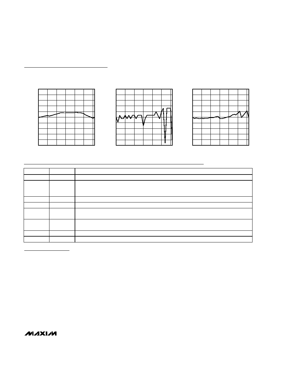
WIPER RESISTANCE vs. WIPER VOLTAGE
MAX5427 toc01
WIPER VOLTAGE (V)
WIPER RESISTANCE (
)
4
3
2
1
100
120
140
160
80
0
5
V
DD
= 3.3V
V
DD
= 5.0V
END-TO-END RESISTANCE PERCENT
CHANGE vs. TEMPERATURE
MAX5427-29 toc02
TEMPERATURE (
°C)
END-TO-END RESISTANCE CHANGE (%)
60
35
10
-15
-0.2
-0.1
0
0.1
0.2
0.3
-0.3
-40
85
MAX5429
MAX5428
MAX5427
W-TO-L RESISTANCE
vs. TAP POSITION
MAX5427-29 toc03
TAP POSITION
W-TO-L RESISTANCE (k
)
25
20
15
10
5
10
20
30
40
50
60
70
80
90
100
0
0
30
MAX5427
MAX5428
MAX5429
SUPPLY CURRENT vs. TEMPERATURE
MAX5427-29 toc04
TEMPERATURE (
°C)
SUPPLY CURRENT (
µ
A)
60
35
10
-15
0.05
0.10
0.15
0.20
0.25
0.30
0
-40
85
V
DD
= 5.0V
V
DD
= 3.3V
R-DNL ERROR vs. INPUT CODE
(MAX5427)
MAX5427-29 toc07
INPUT CODE (DECIMAL)
R-DNL (LSB)
25
20
5
10
15
-0.015
-0.010
-0.005
0
0.005
0.010
0.015
0.020
-0.020
0
30
R-INL ERROR vs. INPUT CODE
(MAX5427)
MAX5427-29 toc08
INPUT CODE (DECIMAL)
R-INL (LSB)
25
20
15
10
5
-0.08
-0.06
-0.04
-0.02
0
0.02
0.04
0.06
0.08
0.10
-0.10
0
30
R-DNL ERROR vs. INPUT CODE
(MAX5428)
MAX5427-29 toc09
INPUT CODE (DECIMAL)
R-DNL (LSB)
25
20
5
10
15
-0.015
-0.010
-0.005
0
0.005
0.010
0.015
0.020
-0.020
0
30
TAP-TO-TAP SWITCHING TRANSIENT
MAX5427-29 toc05
100ns/div
OUTPUT
W
100mV/div
U/D
2V/div
C
L
= 10pF
WIPER TRANSIENT AT POWER-ON
MAX5427-29 toc06
2
µs/div
OUTPUT
W
1V/div
V
DD
2V/div
Detailed Description
The MAX5427/MAX5428/MAX5429 are 100k
/50k/
10k
(end-to-end resistance) digitally controlled poten-
tiometers. They have 32 tap positions that are accessible
to the wiper along the resistor array between H and L.
The wiper (W) position is adjusted sequentially through
the tap positions using a simple 2-wire interface. These
digital potentiometers have an optional one-time pro-
grammable feature that sets the POR position of the
wiper. The 2-wire interface can then be disabled, perma-
nently preventing unwanted adjustment.
Digital Interface Operation
The MAX5427/MAX5428/MAX5429 have two modes of
operation when the serial interface is active: increment
mode and decrement mode. The serial interface is only
active when CS is low.
The CS and U/D inputs control the position of the wiper
along the resistor array. When CS transitions from high
to low, the part goes into increment mode if U/D is high
(Figure 2), and into decrement mode if U/D is low
(Figure 3). Once the mode is set, the device remains in
that mode until CS goes high. A low-to-high transition at
the U/D increments or decrements the wiper position
depending on the current mode.
When the CS input transitions to high (when serial inter-
face is inactive) and U/D is low, the wiper increments or
decrements one position. If U/D is high when CS transi-
tions to high, the wiper remains in the same position.
MAX5427/MAX5428/MAX5429
One-Time Programmable, Linear-Taper
Digital Potentiometers
_______________________________________________________________________________________
5
Pin Description
Typical Operating Characteristics (continued)
(V
DD
= 5.0V, T
A
= +25°C, unless otherwise noted.)
R-INL ERROR vs. INPUT CODE
(MAX5428)
MAX5427-29 toc10
INPUT CODE (DECIMAL)
R-INL (LSB)
25
20
15
10
5
-0.08
-0.06
-0.04
-0.02
0
0.02
0.04
0.06
0.08
0.10
-0.10
0
30
R-DNL ERROR vs. INPUT CODE
(MAX5429)
MAX5427-29 toc11
INPUT CODE (DECIMAL)
R-DNL (LSB)
25
20
15
10
5
-0.020
-0.015
-0.010
-0.005
0
0.005
0.010
0.015
0.020
0.025
-0.025
0
30
R-INL ERROR vs. INPUT CODE
(MAX5429)
MAX5427-29 toc12
INPUT CODE (DECIMAL)
R-INL (LSB)
25
20
15
10
5
-0.08
-0.06
-0.04
-0.02
0
0.02
0.04
0.06
0.08
0.10
-0.10
0
30
PIN
NAME
FUNCTION
1
W
Wiper Connection
2
CS
Chip-Select Input. A high-to-low CS transition determines the mode: increment if U/D is high, or
decrement if U/D is low. CS is also used for one-time programming (see the One-Time Programming
section).
3
V
DD
Power-Supply Voltage
4
GND
Ground
5
V
PP
Programming Voltage for One-Time Programming. Connect V
PP
to 10V supply when one-time
programming the device. For normal operation, connect to ground or let float.
6
U/D
Up/Down Control Input. With CS low, a low-to-high transition increments or decrements the wiper
position.
7
L
Low Terminal of Resistor
8
H
High Terminal of Resistor