
General Description
The MAX5128 nonvolatile, single, linear-taper, digital
potentiometer performs the function of a mechanical
potentiometer, but replaces the mechanics with a sim-
ple 2-wire digital interface. The MAX5128 performs the
same function as a discrete potentiometer or variable
resistor and features 128 taps and 22k
end-to-end
resistance. The MAX5128 also features an ultra-small,
2mm x 2mm µDFN package and low 0.5µA (typ) stand-
by supply current, making this device ideal for portable
applications. The MAX5128 operates from a +2.7V to
+5.25V power supply. An integrated nonvolatile memo-
ry recalls the programmed wiper position of the digital
potentiometer. A simple 2-wire up/down interface pro-
grams the wiper position. The digital potentiometer pro-
vides a low 5ppm/°C ratiometric temperature coefficient
and is specified over the extended -40°C to +85°C tem-
perature range.
Applications
V
COM
Adjustment for LCD Panels
Backlight Adjustment
LED Bias Adjustment
Power-Supply Modules
Fiber-Module Bias Setting
Bias Setting for Radios
Portable Consumer Electronics
Features
Ultra-Small, 2mm x 2mm, 8-Pin µDFN Package
Power-On Recall of Wiper Position from
Nonvolatile Memory
22k End-to-End Resistance
128 Tap Positions
5ppm/°C Ratiometric Temperature Coefficient
1.5µA (max) Standby Supply Current
+2.7V to +5.25V Single Supply Operation
80,000 Wiper Store Cycles
50-Year Wiper Data Retention
MAX5128
128-Tap, Nonvolatile, Linear-Taper Digital
Potentiometer in 2mm x 2mm µDFN Package
________________________________________________________________ Maxim Integrated Products
1
19-3929; Rev 0; 1/06
For pricing, delivery, and ordering information, please contact Maxim/Dallas Direct! at
1-888-629-4642, or visit Maxim's website at www.maxim-ic.com.
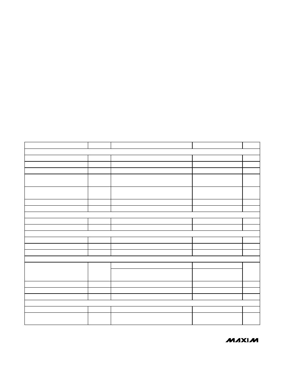
Ordering Information
PART
TEMP
RANGE
PIN -
PA C K A G E
TOP
MARK
PKG
CODE
M AX 5128E LA
-40°C to +85°C
8 µDFN
AAF
L822-1
W
L
SERIAL
INTERFACE
128-POSITION
DECODER
V
CC
GND
DN
UP
7-BIT NV MEMORY
POR
H
128
TAPS
7
7
MAX5128
Functional Diagram
MAX5128
128-Tap, Nonvolatile, Linear-Taper Digital
Potentiometer in 2mm x 2mm µDFN Package
2
_______________________________________________________________________________________
ABSOLUTE MAXIMUM RATINGS
Stresses beyond those listed under "Absolute Maximum Ratings" may cause permanent damage to the device. These are stress ratings only, and functional
operation of the device at these or any other conditions beyond those indicated in the operational sections of the specifications is not implied. Exposure to
absolute maximum rating conditions for extended periods may affect device reliability.
V
CC
to GND ...........................................................-0.3V to +6.0V
UP and DN to GND ....................................-0.3V to (V
CC
+ 0.3V)
H, L, and W to GND....................................-0.3V to (V
CC
+ 0.3V)
Maximum Continuous Current into H, L, and W ..............±0.5mA
Maximum Continuous Current into All Other Pins ............±50mA
Continuous Power Dissipation (T
A
= +70°C)
8-Pin µDFN (derate 4.7mW/°C above +70°C) ........376.5mW
Operating Temperature Range ...........................-40°C to +85°C
Junction Temperature ......................................................+150°C
Storage Temperature Range .............................-60°C to +150°C
Lead Temperature (soldering, 10s) .................................+300°C
ELECTRICAL CHARACTERISTICS
(V
CC
= +2.7V to +5.25V, H = V
CC
, L = GND, T
A
= -40°C to +85°C. Typical values are at V
CC
= +5.0V, T
A
= +25°C, unless otherwise noted.)
(Note 1)
PARAMETER
SYMBOL
CONDITIONS
MIN
TYP
MAX
UNITS
DC PERFORMANCE (voltage-divider mode)
Resolution
N
7
Bits
Integral Nonlinearity
INL
(Note 2)
±1.0
LSB
Differential Nonlinearity
DNL
(Note 2)
±1.0
LSB
End-to-End Resistance
Temperature Coefficient
TC
R
50
ppm/°C
Ratiometric Resistance
Temperature Coefficient
5
ppm/°C
Full-Scale Error
FSE
-3
0
LSB
Zero-Scale Error
ZSE
0
+2
LSB
DC PERFORMANCE (variable-resistor mode)
Integral Nonlinearity
INL
(Note 3)
±1.75
LSB
Differential Nonlinearity
DNL
(Note 3)
±1
LSB
DC PERFORMANCE (resistor characteristics)
Wiper Resistance
R
W
(Note 4)
0.6
0.8
k
Wiper Capacitance
C
W
20
pF
End-to-End Resistance
R
HL
16
22
27
k
DIGITAL INPUTS (UP, DN)
3.4V
V
CC
5.25V
2.4
Input-High Voltage (Note 5)
V
IH
2.7V
V
CC
< 3.4V
0.7 x
V
CC
V
Input-Low Voltage
V
IL
(Note 5)
0.8
V
Input Leakage Current
I
IN
±1
µA
Input Capacitance
C
IN
5
pF
DYNAMIC CHARACTERISTICS
Wiper -3dB Bandwidth
f
3dB
(Note 6)
400
kHz
THD Plus Noise
THD+N
V
H
= 0.3V
RMS
, f = 1kHz, wiper set to
midscale
0.02
%

MAX5128
128-Tap, Nonvolatile, Linear-Taper Digital
Potentiometer in 2mm x 2mm µDFN Package
_______________________________________________________________________________________
3
ELECTRICAL CHARACTERISTICS (continued)
(V
CC
= +2.7V to +5.25V, H = V
CC
, L = GND, T
A
= -40°C to +85°C. Typical values are at V
CC
= +5.0V, T
A
= +25°C, unless otherwise noted.)
(Note 1)
PARAMETER
SYMBOL
CONDITIONS
MIN
TYP
MAX
UNITS
NONVOLATILE MEMORY RELIABILITY
Data Retention
T
A
= +85°C
50
Years
T
A
= +25°C
80,000
Endurance
T
A
= +85°C
50,000
Stores
POWER SUPPLY
Supply Voltage
V
CC
2.70
5.25
V
Average Programming Current
I
PG
During nonvolatile write only;
digital inputs = V
CC
or GND
220
400
µA
Peak Programming Current
I
PK
During nonvolatile write only;
digital inputs = V
CC
or GND
4
mA
Standby Current
I
CC
Digital inputs = V
CC
or GND, T
A
= +25°C
0.5
1.5
µA
TIMING CHARACTERISTICS
(V
CC
= +2.7V to +5.25V, H = V
CC
, L = GND, T
A
= -40°C to +85°C. Typical values are at V
CC
= +5.0V, T
A
= +25°C, unless otherwise noted.)
(See Figures 1, 2, 3, and 4).
PARAMETER
SYMBOL
CONDITIONS
MIN
TYP
MAX
UNITS
ANALOG SECTION
Wiper Settling Time
t
S
(Note 7)
500
ns
DIGITAL SECTION
UP or DN Pulse-Width High
t
PWH
80
ns
UP or DN Pulse-Width Low
t
PWL
80
ns
UP or DN Glitch Immunity
t
IMMU
20
ns
UP Fall to DN Rise Setup or DN
Fall to UP Rise Setup
t
MS1
80
ns
Before Entering NVM-Write
Mode, UP Fall to UP Rise
t
MS2
80
ns
UP Rise to DN Rise Setup when
Entering NVM-Write
t
WS
80
ns
UP Fall to DN Fall Hold or DN Fall
to UP Fall Hold during NVM-
Write
t
WH
0
ns
MAX5128
128-Tap, Nonvolatile, Linear-Taper Digital
Potentiometer in 2mm x 2mm µDFN Package
4
_______________________________________________________________________________________
TIMING CHARACTERISTICS (continued)
(V
CC
= +2.7V to +5.25V, H = V
CC
, L = GND, T
A
= -40°C to +85°C. Typical values are at V
CC
= +5.0V, T
A
= +25°C, unless otherwise noted.)
(See Figures 1, 2, 3, and 4).
PARAMETER
SYMBOL
CONDITIONS
MIN
TYP
MAX
UNITS
NVM-Write Mode Pulse-Width
High
t
WP
80
ns
Write NV Register Busy Time
t
BUSY
14
ms
Power-Up Settling Time
t
ACC
(Note 8)
2
µs
Note 1: All devices are production tested at T
A
= +25°C and are guaranteed by design for T
A
= -40°C to +85°C.
Note 2: The DNL and INL are measured with the potentiometer configured as a voltage-divider with H = V
CC
and L = GND. The
wiper terminal is unloaded and measured with a high input-impedance voltmeter.
Note 3: The DNL and INL are measured with the potentiometer configured as a variable resistor. H is unconnected and L = GND.
For the +5V condition, the wiper terminal is driven with a source current of 200µA and for the +2.7V condition, the wiper ter-
minal is driven with a source current of 100µA.
Note 4: The wiper resistance is measured using the source currents given in Note 3.
Note 5: The device draws higher supply current when the digital inputs are driven with voltages between (V
CC
- 0.5V) and (GND +
0.5V). See Supply Current vs. Digital Input Voltage in the Typical Operating Characteristics.
Note 6: Wiper at midscale with a 10pF load, L = GND, an AC source is applied to H, and the output is measured as 3dB lower than
the DC W/H value in dB.
Note 7: Wiper-settling time is the worst-case 0 to 50% rise time measured between consecutive wiper positions. H = V
CC
, L = GND,
and the wiper terminal is unloaded and measured with a 10pF oscilloscope probe. See the Tap-to-Tap Switching Transient
in the Typical Operating Characteristics section.
Note 8: Power-up settling time is measured from the time V
CC
= 2.7V to the wiper settling to 1 LSB of the final value.
MAX5128
128-Tap, Nonvolatile, Linear-Taper Digital
Potentiometer in 2mm x 2mm µDFN Package
_______________________________________________________________________________________
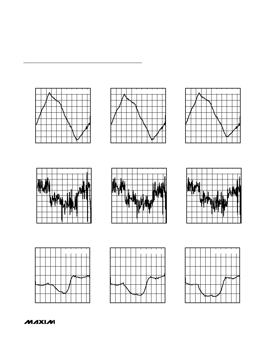
5
-0.06
-0.02
-0.04
0.04
0.02
0
0.06
0.08
0.10
0.12
0
24 36
12
48 60 72 84 96 108 120
INTEGRAL NONLINEARITY
vs. CODE (VOLTAGE-DIVIDER)
MAX5128 toc01
CODE
INL (LSB)
V
CC
= 2.7V, T
A
= -40
°C
-0.06
-0.02
-0.04
0.04
0.02
0
0.06
0.08
0.10
0.12
0
24 36
12
48 60 72 84 96 108 120
INTEGRAL NONLINEARITY
vs. CODE (VOLTAGE-DIVIDER)
MAX5128 toc02
CODE
INL (LSB)
V
CC
= 2.7V, T
A
= +25
°C
-0.06
-0.02
-0.04
0.04
0.02
0
0.06
0.08
0.10
0.12
0
24 36
12
48 60 72 84 96 108 120
INTEGRAL NONLINEARITY
vs. CODE (VOLTAGE-DIVIDER)
MAX5128 toc03
CODE
INL (LSB)
V
CC
= 2.7V, T
A
= +85
°C
-0.010
-0.006
-0.008
0
-0.002
-0.004
0.002
0.004
0.008
0.006
0.010
0
24 36
12
48 60 72 84 96 108 120
MAX5128 toc04
CODE
DNL (LSB)
DIFFERENTIAL NONLINEARITY
vs. CODE (VOLTAGE-DIVIDER)
V
CC
= 2.7V, T
A
= -40
°C
-0.010
-0.006
-0.008
0
-0.002
-0.004
0.002
0.004
0.008
0.006
0.010
0
24 36
12
48 60 72 84 96 108 120
MAX5128 toc05
CODE
DNL (LSB)
DIFFERENTIAL NONLINEARITY
vs. CODE (VOLTAGE-DIVIDER)
V
CC
= 2.7V, T
A
= +25
°C
-0.010
-0.006
-0.008
0
-0.002
-0.004
0.002
0.004
0.008
0.006
0.010
0
24 36
12
48 60 72 84 96 108 120
MAX5128 toc06
CODE
DNL (LSB)
DIFFERENTIAL NONLINEARITY
vs. CODE (VOLTAGE-DIVIDER)
V
CC
= 2.7V, T
A
= +85
°C
-1.5
-0.5
-1.0
0.5
0
1.0
1.5
MAX5128 toc07
INL (LSB)
INTEGRAL NONLINEARITY
vs. CODE (VARIABLE RESISTOR)
0
24 36
12
48 60 72 84 96 108 120
CODE
V
CC
= 2.7V, T
A
= -40
°C
-1.5
-0.5
-1.0
0.5
0
1.0
1.5
MAX5128 toc08
INL (LSB)
INTEGRAL NONLINEARITY
vs. CODE (VARIABLE RESISTOR)
0
24 36
12
48 60 72 84 96 108 120
CODE
V
CC
= 2.7V, T
A
= +25
°C
-1.5
-0.5
-1.0
0.5
0
1.0
1.5
MAX5128 toc09
INL (LSB)
INTEGRAL NONLINEARITY
vs. CODE (VARIABLE RESISTOR)
0
24 36
12
48 60 72 84 96 108 120
CODE
V
CC
= 2.7V, T
A
= +85
°C
Typical Operating Characteristics
(V
CC
= +5.0V, T
A
= +25°C, unless otherwise noted.)