_______________General Description
The MAX5018 is a monolithic, 8-bit digital-to-analog
converter (DAC) capable of accepting video data at
165Msps or 275Msps. Complete with video controls
(sync, blank, reference white (force high), and bright),
the MAX5018 directly drives doubly terminated 50
or
75
loads to standard composite video levels.
Standard setup level is 7.5IRE. The MAX5018 is pin
compatible with the HDAC10180 and the TDC1018,
with improved performance. The MAX5018 contains
data and control input registers, video control logic, ref-
erence buffer, and current switches.
Two performance grades of the MAX5018 are available.
Both are packaged in a 24-pin PDIP in the -20°C to
+85°C industrial temperature range.
________________________Applications
High-Resolution Color or Monochrome Raster
Graphics Displays to 1500 x 1800 Pixels
Medical Electronics: CAT, PET, and MRI Displays
CAD/CAE Workstations
Solids Modeling
General-Purpose, High-Speed Digital-to-Analog
Conversion
Digital Synthesizers
Automated Test Equipment
Digital Transmitters/Modulators
____________________________Features
o
275Msps Conversion Rate (MAX5018A)
165Msps Conversion Rate (MAX5018B)
o
TDC1018 and HDAC10180 Compatible with
Improved Performance
o
RS-343-A Compatible
o
Complete Video Controls: Sync, Blank, Bright,
and Reference White (force high)
o
ECL Compatible
o
Single Power Supply
o
Registered Data and Video Controls
o
Differential Current Outputs
o
ESD-Protected Data and Control Inputs
MAX5018
8-Bit, High-Speed DAC
________________________________________________________________
Maxim Integrated Products
1
19-1204; Rev 0; 3/97
For the latest literature: http://www.maxim-ic.com, or phone 1-800-998-8800
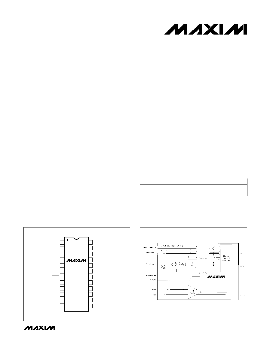
__________________Pin Configuration
24
23
22
21
20
19
18
17
1
2
3
4
5
6
7
8
D4
D5
D6
D7
D0
D1
D2
D3
TOP VIEW
V
EE
Out+
Out-
V
CC
FT
CONV
CONV
V
EE
16
15
14
13
9
10
11
12
COMP
Ref+
Ref-
Sync
BRT
Blank
FH
V
CC
DIP
MAX5018
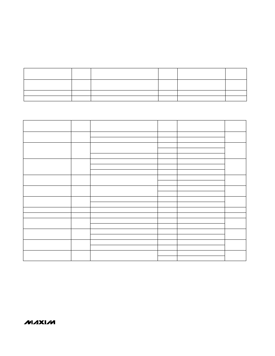
________________Functional Diagram
______________Ordering Information
PART
MAX5018BIPG
MAX5018AIPG
-20°C to +85°C
24 Plastic DIP
-20°C to +85°C
TEMP. RANGE
PIN-PACKAGE
24 Plastic DIP
MAX5018

MAX5018
8-Bit, High-Speed DAC
2
_______________________________________________________________________________________
ABSOLUTE MAXIMUM RATINGS
DC ELECTRICAL CHARACTERISTICS
(V
CC
= ground, V
EE
= -5.2V ±0.3V, C
C
= 0pF, I
SET
= 1.105mA, T
A
= T
MIN
to T
MAX
, unless otherwise noted.)
Stresses beyond those listed under "Absolute Maximum Ratings" may cause permanent damage to the device. These are stress ratings only, and functional
operation of the device at these or any other conditions beyond those indicated in the operational sections of the specifications is not implied. Exposure to
absolute maximum rating conditions for extended periods may affect device reliability.
Supply Voltage
V
EE
(measured to V
CC
)..........................................-7.0V to 0.5V
Input Voltages
CONV, Data, and Controls (measured to V
CC
)........V
EE
to 0.5V
Ref+ (measured to V
CC
) ..........................................V
EE
to 0.5V
Ref- (measured to V
CC
)............................................V
EE
to 0.5V
Operating Temperature Ranges
Ambient .............................................................-20°C to +85°C
Junction..........................................................................+175°C
Lead Temperature (soldering, 10sec) .............................+300°C
Storage Temperature Range .............................-60°C to +150°C
µA
35
120
I
IL
Input Current, Logic Low,
Data and Controls
-0.95
0.95
VI
-0.5
0.5
CONDITIONS
µA
40
120
I
IH
Input Current, Logic High,
Data and Controls
VI
µA
2
60
I
CONV
Input Current, Convert
VI
1.0mA < I
SET
< 1.3mA
% Full Scale
-0.37
0.37
ILE
Integral Linearity Error
VI
1.0mA < I
SET
< 1.3mA
% Full Scale
-0.2
0.2
DLE
Differential Linearity Error
V
0.4
1.2
Convert Voltage,
Differential
V
-0.5
-2.5
Convert Voltage,
Common-Mode Range
V
-1.5
V
IL
Input Voltage, Logic Low
V
-1.0
V
IH
Input Voltage, Logic High
LSB
0.05
0.5
I
OS
Output Offset Current
mA
-45
IO-
(MAX)
Maximum Current,
Negative Output
% Full Scale
-6.5
6.5
Gain Error
mA
45
IO+
(MAX)
Maximum Current,
Positive Output
pF
12
C
OUT
Output Capacitance
k
20
R
OUT
Equivalent Output
Resistance
V
-1.2
1.5
Compliance Voltage,
Negative Output
ppm/°C
150
Gain-Error Tempco
pF
5
C
REF
Input Capacitance,
Ref+, Ref-
V
-1.2
1.5
Compliance Voltage,
Positive Output
UNITS
MIN
TYP
MAX
SYMBOL
PARAMETER
VI
VI
IV
IV
IV
V
VI
VI
VI
VI
V
V
VI
VI
IV
TEST
LEVEL
LSB
LSB
Msps
MAX5018
8-Bit, High-Speed DAC
_______________________________________________________________________________________
3
To 0.2% G.S., R
L
= 25
4.5
MAX5018B
V
MAX5018A
275
t
S
III
10% to 90% G.S., R
L
= 25
1.0
2.0
IV
V
CONDITIONS
10% to 90% G.S., T
A
= T
MIN
to T
MAX
ns
1.6
t
R
Rise Time
III
To 0.8% G.S.
5.5
V
IV
T
A
= T
MIN
to T
MAX
4.5
t
H
T
A
= T
MIN
to T
MAX
ns
2.2
4.0
t
DSC
Clock to Output Delay,
Clocked Mode
III
IV
To 0.2% G.S.
7.0
V
T
A
= T
MIN
to T
MAX
ns
6.0
t
DST
IV
Area = 1/2VT
pV-s
Msps
165
Maximum Conversion Rate
4
A Grade
1.8
Glitch Energy
Convert Pulse Width,
(low or high)
V
B Grade
ns
3.0
t
PWL
,
t
PWH
III
T
A
= +25°C
ns
1.0
MHz
1.0
Reference Bandwidth, -3dB
V
T
A
= T
MIN
to T
MAX
ns
0.5
IV
T
A
= +25°C
0.5
Hold Time, Data and
Controls
III
III
UNITS
MIN
TYP
MAX
SYMBOL
PARAMETER
1.0
III
Setup Time, Data and
Controls
III
3.2
6.0
Data to Output Delay,
Transparent Mode
III
dB
-48
Clock Feedthrough
III
T
A
= T
MIN
to T
MAX
325
IV
TEST
LEVEL
T
A
= T
MIN
to T
MAX
-48
IV
20% to 80% G.S., T
A
= +25°C
V/µs
390
Slew Rate
III
CONDITIONS
mA
155
220
I
EE
Supply Current
pF
3
C
IN
Input Capacitance, Data
and Controls
µA/V
-120
20
120
Power-Supply Sensitivity
UNITS
MIN
TYP
MAX
SYMBOL
PARAMETER
VI
V
VI
TEST
LEVEL
DC ELECTRICAL CHARACTERISTICS (continued)
(V
CC
= ground, V
EE
= -5.2V ±0.3V, C
C
= 0pF, I
SET
= 1.105mA, T
A
= T
MIN
to T
MAX
, unless otherwise noted.)
AC ELECTRICAL CHARACTERISTICS
(R
L
= 37.5
, C
L
= 5pF, I
SET
= 1.105mA, T
A
= +25°C, unless otherwise noted.)
t
SI
ns
Current Settling Time,
Clocked Mode
MAX5018
8-Bit, High-Speed DAC
4
_______________________________________________________________________________________
Data Bit 0 (LSB)
D0
4
Convert Clock Input
CONV
6
Negative Supply
V
EE
5, 20
Register Feedthrough Control
FT
8
Data Force-High Control
FH
10
Positive Supply
V
CC
9, 17
Convert-Clock-Input Complement
CONV
7
Video Bright Input
BRT
12
Reference Current, Negative Input
Ref-
14
Video Sync Input
Sync
13
Compensation Input
COMP
16
PIN
Output Current Negative
Out-
18
Data Bits 3, 2, and 1
D3, D2, D1
1, 2, 3
FUNCTION
NAME
Reference Current, Positive Input
Ref+
15
Video Blank Input
Blank
11
Data Bits 6, 5, and 4
D6, D5, D4
22, 23, 24
Data Bit 7 (MSB)
D7
21
Output Current Positive
Out+
19
______________________________________________________________Pin Description
TEST-LEVEL CODES
All electrical characteristics are subject to
the following conditions:
All parameters having min/max specifica-
tions are guaranteed. The Test Level column
indicates the specific device testing actually
performed during production and Quality
Assurance inspection. Any blank section in
the data column indicates that the specifica-
tion is not tested at the specified condition.
Unless otherwise noted, all tests are pulsed
tests; therefore, T
j
= T
C
= T
A
.
TEST LEVEL
I
II
III
IV
V
VI
TEST PROCEDURE
100% production tested at the specified temperature.
100% production tested at T
A
= +25°C, and sample
tested at the specified temperatures.
QA sample tested at only the specified temperatures.
Parameter is guaranteed (but not tested) by design
and characterization data.
Parameter is a typical value for reference only.
100% production tested at T
A
= +25°C. Parameter is
guaranteed over specified temperature range.
_______________Detailed Description
The MAX5018 is an ultra-high-speed video digital-to-
analog converter (DAC) capable of up to 275Msps con-
version rates. This high speed makes the device
suitable for driving 1500 x 1800 pixel displays at 70Hz
to 90Hz update rates.
The MAX5018 is separated into different conversion-
rate categories, as shown in Table 1.
The MAX5018 has ECL logic-level-compatible video
controls and data inputs. The complementary analog
output currents produced by the devices are propor-
tional to the product of the digital control and data
inputs in conjunction with the analog reference current.
The MAX5018 is segmented so that the input data's
four MSBs are separated into a parallel thermometer
code. From here, fifteen identical current sinks are driv-
en to fabricate sixteen coarse output levels. The
remaining four LSBs drive four binary-weighted current
switches.
MSB currents are then summed with the LSBs that con-
tribute one-sixteenth of full-scale to provide the 256 dis-
tinct analog output levels.
The video-control inputs drive weighted current sinks,
which are added to the output current to produce com-
posite video-output levels. These controls (sync, blank,
reference white (force high), and bright) are required in
video applications.
A feature that similar video DACs do not have is feed-
through control. The feedthrough pin (FT) allows regis-
tered or unregistered operation of the video control and
data inputs. In registered mode, the composite func-
tions are latched to the pixel data to prevent screen-
edge distortions (generally found on unregistered video
DACs).
__________Applications Information
General
Figure 1 shows a typical application using the MAX5018
in a color-raster circuit. The MAX5018 requires few exter-
nal components and is extremely easy to use. The
MAX5018's very high operating speeds require good cir-
cuit layout, supply decoupling, and proper transmission-
line design. For best performance, note the following
considerations.
Input Considerations
Video-input data and controls can be directly con-
nected to the MAX5018. Note that all ECL inputs are
terminated as closely to the device as possible to
reduce ringing, crosstalk, and reflections. Maxim rec-
ommends that stripline or microstrip techniques be
used for all ECL interfaces. A convenient and common-
ly used microstrip impedance is about 130
, which is
easily terminated using a 330
resistor to V
EE
and a
220
resistor to ground. This arrangement gives a
Thevenin-equivalent termination of 130
to -2V without
the need for a -2V supply. Standard single in-line pack-
age (SIP) 220/330 resistor networks are available for
this purpose.
Figure 2 shows equivalent input circuits.
Output Considerations
The analog outputs are designed to directly drive a
dual 50
or 75
load-transmission system as shown in
Figure 1. The MAX5018 output source impedances are
high-impedance current sinks. The load impedance
(R
L
) must be 25
or 37.5
to attain standard RS-343-A
video levels. Any deviation from this impedance affects
the resulting video output levels proportionally. As with
the data interface, it is important that all analog trans-
mission lines have matched impedance throughout,
including connectors and transitions between printed
wiring and coaxial cable. The combination of matched
source-termination resistor R
S
and load terminator R
L
minimizes reflections of both forward and reverse trav-
eling waves in the analog transmission system.
Power Considerations
The MAX5018 has two analog power-supply pins and
operates from a standard -5.2V single supply. Proper
supply bypassing augments the MAX5018's inherent
supply-noise-rejection characteristics. As shown in
Figure 1, each supply pin should be bypassed as
close to the device as possible with 0.01µF and 10µF
capacitors.
MAX5018
8-Bit, High-Speed DAC
_______________________________________________________________________________________
5
PART
UPDATE
COMMENTS
MAX5018A
275Msps
Suitable for 1200 x 1500 to
1500 x 1800 displays at
60Hz to 90Hz update rate.
MAX5018B
165Msps
Suitable for 1024 x 1280 to
1200 x 1500 displays at
60Hz to 90Hz update rate.
Table 1. The MAX5018 Family and
Speed Designations