
General Description
The MAX4843MAX4846 overvoltage protection con-
trollers protect low-voltage systems against high-voltage
faults of up to 28V. When the input voltage exceeds the
overvoltage threshold, these devices turn off a low-cost,
external n-channel FET(s) to prevent damage to the pro-
tected components. An internal charge pump eliminates
the need for external capacitors and drives the FET gate
for a simple, robust solution.
The overvoltage trip level is set to 7.4V (MAX4843),
6.35V (MAX4844), 5.8V (MAX4845), or 4.65V
(MAX4846). When the input voltage drops below the
undervoltage lockout (UVLO) threshold, the devices
enter a low standby current mode (10 µA). The
MAX4843/MAX4844/ MAX4845 have a UVLO threshold
of 4.15V, and the MAX4846 has a UVLO threshold of
2.5V. In addition to the single FET configuration, the
devices can be configured with back-to-back external
FETs to prevent currents from being back-driven into the
adapter.
An additional feature includes a ±15kV ESD-protected
input when bypassed with a 1µF capacitor to ground. All
devices are offered in a small (1.5mm x 1.0mm) 6-pin
µDFN package and are specified for operation over the
-40°C to +85°C temperature range.
Applications
Cell Phones
Digital Still Cameras
PDAs and Palmtop Devices
MP3 Players
Features
o
Overvoltage Protection Up to 28V
o
Preset 7.4V, 6.35V, 5.8V, or 4.65V Overvoltage Trip
Level
o
Low (10µA) Undervoltage Lockout Standby
Current
o
Drives Low-Cost n MOSFET
o
Internal 50ms Startup Delay
o
Internal Charge Pump
o
Overvoltage Fault FLAG Indicator
o
6-Pin (1.5mm x 1.0mm) µDFN Package
MAX4843MAX4846
Overvoltage Protection Controllers with
Low Standby Current
________________________________________________________________ Maxim Integrated Products
1
GND
GATE
FLAG
1
6
N.C.
5
N.C.
IN
MAX4843
MAX4846
µ
DFN
TOP VIEW
2
3
4
PART
*
PIN-
PACKAGE
UVLO
(V)
OVLO
(V)
TOP
MARK
MAX4843
ELT
6 µDFN
4.15
7.40
BE
MAX4844
ELT
6 µDFN
4.15
6.35
BF
MAX4845
ELT
6 µDFN
4.15
5.80
BG
MAX4846
ELT
6 µDFN
2.50
4.65
BH
Pin Configuration
Ordering Information
MAX4843
MAX4846
4
OUTPUT
GATE
FLAG
V
IO
N
3
1
IN
2
GND
INPUT
+1.2V TO +28V
1
µ
F
Typical Operating Circuit
19-3649; Rev 0; 4/05
For pricing, delivery, and ordering information, please contact Maxim/Dallas Direct! at
1-888-629-4642, or visit Maxim's website at www.maxim-ic.com.
*All devices are specified over the -40°C to +85°C temperature
range.

MAX4843MAX4846
Overvoltage Protection Controllers with
Low Standby Current
2
_______________________________________________________________________________________
ABSOLUTE MAXIMUM RATINGS
ELECTRICAL CHARACTERISTICS
(V
IN
= +5V for MAX4843/MAX4844/MAX4845, V
IN
= +4V for MAX4846, C
GATE
= 500pF, T
A
= -40°C to +85°C, unless otherwise
noted. Typical values are at T
A
= +25°C.) (Note 1)
Stresses beyond those listed under "Absolute Maximum Ratings" may cause permanent damage to the device. These are stress ratings only, and functional
operation of the device at these or any other conditions beyond those indicated in the operational sections of the specifications is not implied. Exposure to
absolute maximum rating conditions for extended periods may affect device reliability.
IN to GND ..............................................................-0.3V to +30V
GATE to GND ........................................................-0.3V to +12V
FLAG to GND ..........................................................-0.3V to +6V
Continuous Power Dissipation (T
A
= +70°C)
6-Pin µDFN (derate 2.1mW/°C above +70°C) .........167.7mW
Operating Temperature Range ..........................-40°C to +85°C
Junction Temperature .................................................... +150°C
Storage Temperature Range ............................-65°C to +150°C
Lead Temperature (soldering, 10s) ................................+300°C
PARAMETER
SYMBOL
CONDITIONS
MIN
TYP
MAX
UNITS
Input Voltage Range
V
IN
1.2
28.0
V
MAX4843/MAX4844/MAX4845
3.9
4.15
4.4
Undervoltage Lockout Threshold
UVLO
V
IN
falling
MAX4846
2.3
2.5
2.7
V
MAX4843/MAX4844/MAX4845
41
Undervoltage Lockout Hysteresis
MAX4846
25
mV
MAX4843
7.0
7.4
7.8
MAX4844
6.0
6.35
6.7
MAX4845
5.5
5.8
6.1
Overvoltage Trip Level
OVLO
V
IN
rising
MAX4846
4.35
4.65
4.95
V
MAX4843
75
MAX4844
65
MAX4845
55
Overvoltage Lockout Hysteresis
MAX4846
50
mV
MAX4843/MAX4844/MAX4845
70
120
IN Supply Current
I
IN
MAX4846
60
110
µA
V
IN
= 3.8V
MAX4843/MAX4844/MAX4845
10
22
UVLO Supply Current
I
UVLO
V
IN
= 2.2V
MAX4846
8
18
µA
MAX4843/MAX4844/MAX4845
9
9.83
10
Gate Voltage
V
GATE
1µA load
MAX4846
7.5
7.85
8.0
V
GATE Pulldown Current
I
PD
V
IN
> OVLO, V
GATE
= 5.5V
10
27
mA
FLAG Output Low Voltage
V
OL
I
SINK
= 1mA, FLAG deasserted
0.4
V
FLAG Leakage Current
V
FLAG
= 5.5V, FLAG asserted
1
µA

MAX4843MAX4846
Overvoltage Protection Controllers with
Low Standby Current
_______________________________________________________________________________________
3
Note 1:
All devices are 100% tested at +25°C. Electrical limits across the full temperature range are guaranteed by design and correlation.
ELECTRICAL CHARACTERISTICS (continued)
(V
IN
= +5V for MAX4843/MAX4844/MAX4845, V
IN
= +4V for MAX4846, C
GATE
= 500pF, T
A
= -40°C to +85°C, unless otherwise
noted. Typical values are at T
A
= +25°C.) (Note 1)
PARAMETER
SYMBOL
CONDITIONS
MIN
TYP
MAX
UNITS
TIMING
Startup Delay
t
START
V
IN
= UVLO rising to V
GATE
= 0.3V rising
(Figure 1)
20
50
80
ms
FLAG Blanking Time
t
BLANK
V
GATE
= 0.3V rising to V
FLAG
= 0.3V falling
(Figure 1)
20
50
80
ms
Gate Turn-On Time
t
GON
V
GATE
= 0.3V to 8V
(MAX4843/MAX4844/MAX4845),
V
GATE
= 0.3V to 7V (MAX4846) (Figure 1)
10
ms
Gate Turn-Off Time
t
GOFF
V
IN
rising at 1V/µs from 5V to 8V
(MAX4843/MAX4844/MAX4845)
or from 4V to 7V (MAX4846)
to V
GATE
= 0.3V (Figure 2)
6
20
µs
FLAG Assertion Delay
t
FLAG
V
IN
rising at 1V/µs from 5V to 8V
(MAX4843/MAX4844/MAX4845)
or from 4V to 7V (MAX4846), to V
FLAG
=
2.4V, R
FLAG
= 10k
to 3V (Figure 2)
5.8
µs
Initial Overvoltage Fault Delay
t
OVP
V
IN
rising at 1V/µs from 0V to 9V, time from
V
IN
= 5V to I
GATE
= 80% of I
PD
(Figure 3)
1.5
µs
Typical Operating Characteristics
(V
IN
= +5V for MAX4843/MAX4844/MAX4845, V
IN
= +4V for MAX4846, T
A
= +25°C, unless otherwise noted.)
SUPPLY CURRENT vs. SUPPLY VOLTAGE
(MAX4843)
MAX4843-46 toc01
SUPPLY VOLTAGE (V)
SUPPLY CURRENT (
µ
A)
25
20
15
10
5
20
40
60
80
100
0
0
30
REVERSE CURRENT vs. OUTPUT VOLTAGE
(MAX4843)
MAX4843-46 toc02
OUTPUT VOLTAGE (V)
REVERSE CURRENT (
µ
A)
7
6
4
5
3
2
0.00001
0.0001
0.001
0.01
0.1
1
10
100
1000
0.000001
1
BACK-TO-BACK FET
SINGLE FET
GATE VOLTAGE vs. INPUT VOLTAGE
(MAX4843/MAX4844/MAX4845)
MAX4843-46 toc03
INPUT VOLTAGE (V)
GATE VOLTAGE (V)
7
6
5
4
3
6
9
12
15
0
3
8
MAX4843
MAX4844
MAX4845

MAX4843MAX4846
Overvoltage Protection Controllers with
Low Standby Current
4
_______________________________________________________________________________________
Typical Operating Characteristics (continued)
(V
IN
= +5V for MAX4843/MAX4844/MAX4845, V
IN
= +4V for MAX4846, T
A
= +25°C, unless otherwise noted.)
GATE VOLTAGE vs. INPUT VOLTAGE
(MAX4846)
MAX4843-46 toc04
INPUT VOLTAGE (V)
GATE VOLTAGE (V)
5
4
3
2
2
4
6
8
10
0
1
6
GATE VOLTAGE vs. INPUT VOLTAGE
(MAX4843)
MAX4843-46 toc05
INPUT VOLTAGE (V)
GATE VOLTAGE (V)
7
6
5
4
9.75
10.00
10.25
10.50
9.50
3
8
GATE CURRENT = 0
GATE
CURRENT = 1
µ
A
POWER-UP RESPONSE
MAX4843-46 toc06
20ms/DIV
5V/DIV
V
IN
V
GATE
V
FLAG
5V/DIV
0
0
5V/DIV
0
POWER-UP RESPONSE
MAX4843-46 toc07
20ms/DIV
5V/DIV
V
IN
V
OUT
I
IN
V
FLAG
5V/DIV
0
0
1A/DIV
0
5V/DIV
0
OVERVOLTAGE RESPONSE
MAX4843-46 toc08
4
µ
s/DIV
5V/DIV
V
IN
V
GATE
I
GATE
V
FLAG
10V/DIV
0
8V
0
10mA/DIV
0
5V/DIV
0
POWER-UP OVERVOLTAGE RESPONSE
MAX4843-46 toc09
20
µ
s/DIV
5V/DIV
V
IN
V
GATE
V
FLAG
2V/DIV
0
8V
0
5V/DIV
0
PIN
NAME
FUNCTION
1
IN
Voltage Input. IN is both the power-supply input and the overvoltage sense input. Bypass IN to GND with
a 1µF capacitor or larger.
2
GND
Ground
3
FLAG
Fault Indication Output. FLAG is asserted high during undervoltage lockout and overvoltage lockout
conditions. FLAG is deasserted during normal operation. FLAG is an open-drain output.
4
GATE
Gate-Drive Output. GATE is the output of an on-chip charge pump. When V
UVLO
< V
IN
< V
OVLO
, GATE is
driven high to turn on the external n-channel MOSFET(s).
5, 6
N.C.
No Connection. Not internally connected.
Pin Description
MAX4843MAX4846
Overvoltage Protection Controllers with
Low Standby Current
_______________________________________________________________________________________
5
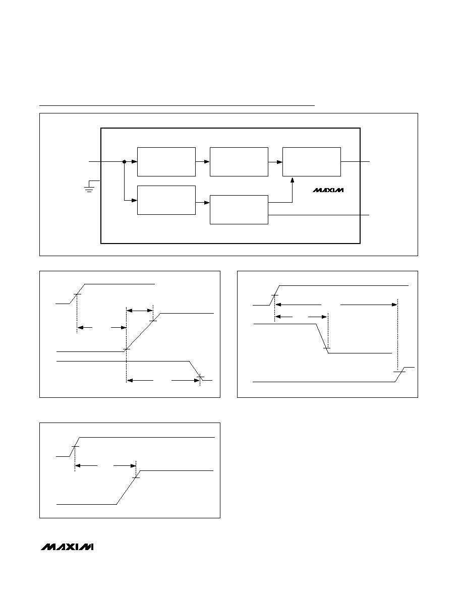
Functional Diagram
Figure 2. Shutdown Timing Diagram
t
OVP
80%
V
IN
0V
I
GATE
V
OVLO
MAX4843
MAX4846
GATE DRIVER
GATE
FLAG
2x CHARGE
PUMP
5.5V
REGULATOR
IN
GND
UVLO AND
OVLO
DETECTOR
CONTROL
LOGIC AND
TIMER
t
FLAG
t
GOFF
0.3V
2.4V
V
IN
V
OVLO
5V
V
GATE
V
FLAG
V
UVLO
t
GON
t
BLANK
t
START
5V
8V
0.3V
0.3V
V
IN
V
GATE
V
FLAG
Figure 1. Startup Timing Diagram
Figure 3. Power-Up Overvoltage Timing Diagram