Äîêóìåíòàöèÿ è îïèñàíèÿ www.docs.chipfind.ru
General Description
The MAX4737/MAX4738/MAX4739 low-voltage, low on-
resistance (R
ON
), quad single-pole/single throw (SPST)
analog switches operate from a single +1.8V to +5.5V
supply. These devices are designed for USB 1.1 and
audio switching applications.
The MAX4737/MAX4738/MAX4739 feature 4.5
R
ON
(max) with 1.2
flatness and 0.4 matching between
channels. These new switches feature guaranteed
operation from +1.8V to +5.5V and are fully specified at
3V and 5V. These switches offer break-before-make
switching (1ns) with t
ON
<80ns and t
OFF
<40ns at
+2.7V. The digital logic inputs are +1.8V logic compati-
ble with a +2.7V to +3.6V supply.
These switches are packaged in a chip-scale package
(UCSPTM), significantly reducing the required PC board
area. The chip occupies only a 2mm
2mm area and
has a 4
4 bump array with a bump pitch of 0.5mm.
These switches are also available in a 14-pin TSSOP
package.
Applications
Battery-Operated Equipment
Audio/Video-Signal Routing
Low-Voltage Data-Acquisition Systems
Sample-and-Hold Circuits
Data-Acquisition Systems
Communications Circuits
Features
o USB 1.1 Signal Switching
o 2ns (max) Differential Skew
o -3dB Bandwidth: >300MHz
o Low 20pF On-Channel Capacitance
o Low R
ON
4.5
(max) (+3V Supply)
3
(max) (+5V Supply)
o 0.4 (max) R
ON
Match (+3V Supply)
o 1.2 (max) R
ON
Flatness (+3V Supply)
o <0.5nA Leakage Current at +25°C
o High Off-Isolation: -55dB (10MHz)
o Low Crosstalk: -80dB (10MHz)
o Low Distortion: 0.03%
o +1.8V CMOS-Logic Compatible
o Single-Supply Operation from +1.8V to +5.5V
o Rail-to-Rail
®
Signal Handling
MAX4737/MAX4738/MAX4739
4.5
Quad SPST Analog Switches in UCSP
________________________________________________________________ Maxim Integrated Products
1
Ordering Information
19-2633; Rev 0; 10/02
For pricing, delivery, and ordering information, please contact Maxim/Dallas Direct! at
1-888-629-4642, or visit Maxim's website at www.maxim-ic.com.
PART
TEMP RANGE
PIN/BUMP-
PACKAGE
TOP
MARK
MAX4737EUD
-40°C to +85°C
14 TSSOP
--
MAX4737EBE-T*
-40°C to +85°C
16 UCSP-16
4737
MAX4738EUD
-40°C to +85°C
14 TSSOP
--
MAX4738EBE-T*
-40°C to +85°C
16 UCSP-16
4738
MAX4739EUD
-40°C to +85°C
14 TSSOP
--
MAX4739EBE-T*
-40°C to +85°C
16 UCSP-16
4739
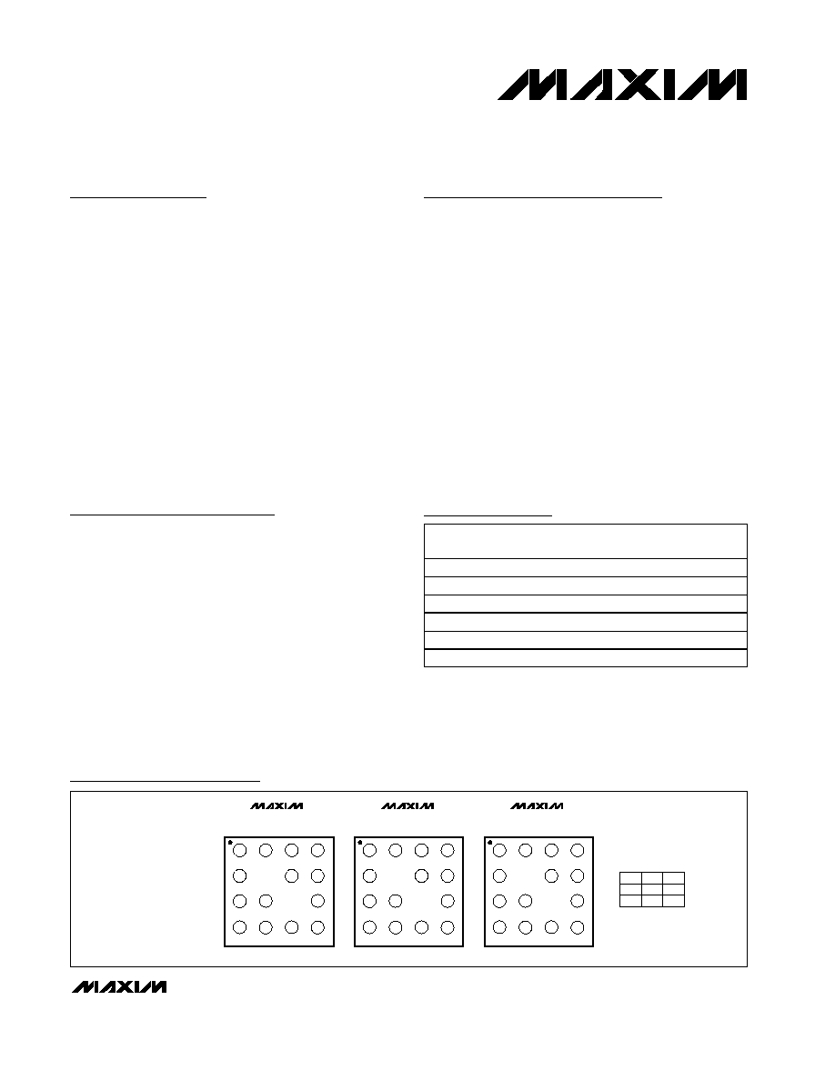
C
D
B
A
1
2
3
4
IN2
COM2
COM1
NO2
IN3
V+
NO1
NO3
GND
IN1
COM3
COM4
NO4
IN4
TOP VIEW
(BUMPS SIDE DOWN)
MAX4737
C
D
B
A
1
2
3
4
IN2
COM2
COM1
NC2
IN3
V+
NC1
NC3
GND
IN1
COM3
COM4
NC4
IN4
MAX4738
C
D
B
A
1
2
3
4
IN2
COM2
COM1
NC2
IN3
V+
NO1
NO3
GND
IN1
COM3
COM4
NC4
IN4
MAX4739
IN_
LOW
HIGH
NO_
OFF
ON
NC_
ON
OFF
UCSP
UCSP
UCSP
Pin Configurations/Functional Diagrams/Truth Tables
UCSP is a trademark of Maxim Integrated Products, Inc.
Rail-to-Rail is a registered trademark of Nippon Motorola, Ltd.
Note: UCSP package requires special solder temperature pro-
file described in the Absolute Maximum Ratings section.
*UCSP reliability is integrally linked to the user's assembly meth-
ods, circuit board material, and environment. See the UCSP reli-
ability notice in the UCSP Reliability section of this data sheet for
more information.
MAX4737/MAX4738/MAX4739
4.5
Quad SPST Analog Switches in UCSP
2
_______________________________________________________________________________________
ABSOLUTE MAXIMUM RATINGS
ELECTRICAL CHARACTERISTICS--Single +3V Supply
(V+ = +2.7V to +3.6V, V
IH
= +1.4V, V
IL
= +0.5V, T
A
= T
MIN
to T
MAX
, unless otherwise noted. Typical values are at V+ = +3.0V,
T
A
= +25°C, unless otherwise noted.) (Notes 3, 4)
Stresses beyond those listed under "Absolute Maximum Ratings" may cause permanent damage to the device. These are stress ratings only, and functional
operation of the device at these or any other conditions beyond those indicated in the operational sections of the specifications is not implied. Exposure to
absolute maximum rating conditions for extended periods may affect device reliability.
(All Voltages Referenced to GND)
V+, IN_...................................................................-0.3V to +6.0V
COM_, NO_, NC_ (Note 1) ...........................-0.3V to (V+ + 0.3V)
Continuous Current COM_, NO_, NC_ ...........................±100mA
Peak Current COM_, NO_, NC_
(pulsed at 1ms, 10% duty cycle)................................±200mA
Continuous Power Dissipation (T
A
= +70°C)
14-Pin TSSOP (derate 6.3mW/°C above +70°C) .........500mW
16-Bump UCSP (derate 8.3mW/°C above +70°C) ......659mW
ESD Method 3015.7 .............................................................>2kV
Operating Temperature Range ...........................-40°C to +85°C
Junction Temperature ......................................................+150°C
Storage Temperature Range .............................-65°C to +150°C
Lead Temperature (soldering, 10s) .................................+300°C
Bump Temperature (soldering) (Note 2)
Infrared (15s) ...............................................................+220°C
Vapor Phase (60s) .......................................................+215°C
Note 1: Signals on COM_, NO_, or NC_ exceeding V+ or GND are clamped by internal diodes. Limit forward-diode current to maxi-
mum current rating.
Note 2: This device is constructed using a unique set of packaging techniques that impose a limit on the thermal profile the device
can be exposed to during board level solder attach and rework. This limit permits only the use of the solder profiles recom-
mended in the industry standard specification, JEDEC 020A, paragraph 7.6, table 3 for IR/VPR and convection reflow.
Preheating is required. Hand or wave soldering is not allowed.
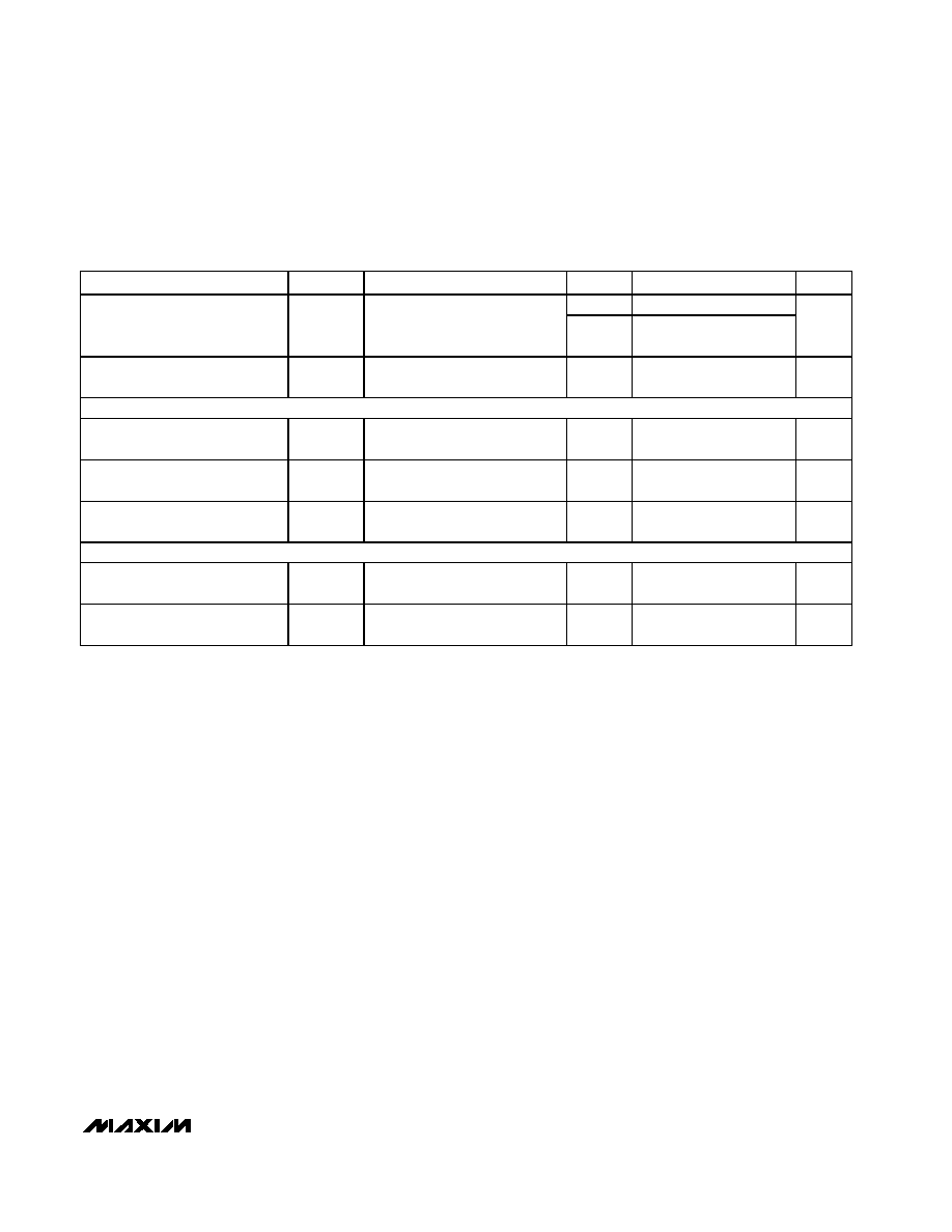
PARAMETER
SYMBOL
CONDITIONS
T
A
MIN
TYP
MAX
UNITS
Analog Signal Range
V
COM_
,
V
NO_
, V
NC_
0
V+
V
ANALOG SWITCH
+25°C
3.0
4.5
On-Resistance (Note 5)
R
ON
V+ = 2.7V, I
COM_
= 10mA;
V
NO_
or V
NC_
= 1.5V
T
MIN
to
T
MAX
5
+25°C
0.1
0.4
On-Resistance Match Between
Channels (Notes 5, 6)
R
ON
V+ = 2.7V, I
COM_
= 10mA;
V
NO_
or V
NC_
= 1.5V
T
MIN
to
T
MAX
0.5
+25°C
0.6
1.2
On-Resistance Flatness (Note 7)
R
FLAT(ON)
V+ = 2.7V, I
COM_
= 10mA;
V
NO_
or V
NC_
= 1.0V, 1.5V, 2.0V
T
MIN
to
T
MAX
1.5
+25°C
-0.5
+0.01
+0.5
NO_, NC_ Off-Leakage Current
(Note 8)
I
NO_(OFF)
,
I
NC_(OFF)
V+ = 3.6V, V
COM_
= 0.3V, 3.3V;
V
NO_
or V
NC_
= 3.3V, 0.3V
T
MIN
to
T
MAX
-1
+1
nA
+25°C
-0.5
+0.01
+0.5
COM_ Off-Leakage Current
(Note 8)
I
C OM_( OFF)
V+ = 3.6V, V
COM_
= 0.3V, 3.3V;
V
NO_
or V
NC_
= 3.3V, 0.3V
T
MIN
to
T
MAX
-1
+1
nA
+25°C
-1
+0.01
+1
COM_ On-Leakage Current
(Note 8)
I
COM_(ON)
V+ = 3.6V, V
COM_
= 0.3V, 3.3V;
V
NO_
or V
NC_
= 0.3V, 3.3V, or
floating
T
MIN
to
T
MAX
-2
+2
nA
MAX4737/MAX4738/MAX4739
4.5
Quad SPST Analog Switches in UCSP
_______________________________________________________________________________________
3
ELECTRICAL CHARACTERISTICS--Single +3V Supply (continued)
(V+ = +2.7V to +3.6V, V
IH
= +1.4V, V
IL
= +0.5V, T
A
= T
MIN
to T
MAX
, unless otherwise noted. Typical values are at V+ = +3.0V,
T
A
= +25°C, unless otherwise noted.) (Notes 3, 4)
PARAMETER
SYMBOL
CONDITIONS
T
A
MIN
TYP
MAX
UNITS
DYNAMIC CHARACTERISTICS
+25°C
40
80
Turn-On Time
t
ON
V
NO_
, V
NC_
= 1.5V;
R
L
= 300
, C
L
= 35pF, Figure 1
T
MIN
to
T
MAX
100
ns
+25°C
20
40
Turn-Off Time
t
OFF
V
NO_
, V
NC_
= 1.5V;
R
L
= 300
, C
L
= 35pF, Figure 1
T
MIN
to
T
MAX
50
ns
+25°C
8
Break-Before-Make Time Delay
(MAX4739 Only) (Note 8)
t
BBM
V
NO_
, V
NC_
= 1.5V;
R
L
= 300
, C
L
= 35pF, Figure 2
T
MIN
to
T
MAX
1
ns
Skew (Note 8)
t
SKEW
R
S
= 39
, C
L
= 50pF, Figure 3
T
MIN
to
T
MAX
0.15
2
ns
Charge Injection
Q
V
GEN
= 2V, R
GEN
= 0
,
C
L
= 1.0nF, Figure 4
+25°C
5
pC
f = 10MHz; V
NO_
, V
NC_
= 1V
P-P
;
R
L
= 50
, C
L
= 5pF, Figure 5a
-55
Off-Isolation (Note 9)
V
ISO
f = 1MHz; V
NO_
, V
NC_
= 1V
P-P
;
R
L
= 50
, C
L
= 5pF, Figure 5a
+25°C
-80
dB
f = 10MHz; V
NO_
, V
NC_
= 1V
P-P
;
R
L
= 50
, C
L
= 5pF, Figure 5b
-80
Crosstalk (Note 10)
V
CT
f = 1MHz; V
NO_
, V
NC_
= 1V
P-P
;
R
L
= 50
, C
L
= 5pF, Figure 5b
+25°C
-110
dB
On-Channel -3dB Bandwidth
BW
Signal = 0dBm, C
L
= 5pF, 50
in and out, Figure 5a
+25°C
300
MHz
Total Harmonic Distortion
THD
R
L
= 600
+25°C
0.03
%
NO_,
NC_ Off-Capacitance
C
NO_(OFF)
,
C
NC_(OFF)
f = 1MHz, Figure 6
+25°C
9
pF
Switch On-Capacitance
C
ON
f = 1MHz, Figure 6
+25°C
15
pF
DIGITAL I/O
Input Logic High Voltage
V
IH
T
MIN
to
T
MAX
1.4
V
Input Logic Low Voltage
V
IL
T
MIN
to
T
MAX
0.5
V
Input Leakage Current
I
IN
V+ = 3.6V, V
IN_
= 0 or 5.5V
T
MIN
to
T
MAX
-0.1
+0.1
µA
MAX4737/MAX4738/MAX4739
4.5
Quad SPST Analog Switches in UCSP
4
_______________________________________________________________________________________
ELECTRICAL CHARACTERISTICS--Single +5V Supply
(V+ = +4.2V to +5.5V, V
IH
= +2.0V, V
IL
= +0.8V, T
A
= T
MIN
to T
MAX
, unless otherwise noted. Typical values are at V+ = +5.0V,
T
A
= +25°C, unless otherwise noted.) (Notes 3, 4)
PARAMETER
SYMBOL
CONDITIONS
T
A
MIN
TYP
MAX
UNITS
Analog Signal Range
V
COM_
,
V
NO_
, V
NC_
T
MIN
to
T
MAX
0
V+
V
ANALOG SWITCH
+25°C
1.7
3.0
On-Resistance (Note 5)
R
ON
V+ = 4.2V; I
COM_
= 10mA;
V
NO_
or V
NC_
= 3.5V
T
MIN
to
T
MAX
35
+25°C
0.1
0.3
On-Resistance Match Between
Channels (Notes 5, 6)
R
ON
V+ = 4.2V; I
COM_
= 10mA;
V
NO_
or V
NC_
= 3.5V
T
MIN
to
T
MAX
0.4
+25°C
0.4
1.2
On-Resistance Flatness (Note 7)
R
FLAT(ON)
V+ = 4.2V; I
COM_
= 10mA;
V
NO_
or V
NC_
= 1.0V, 2.0V, 3.5V
T
MIN
to
T
MAX
1.5
+25°C
-0.5
0.01
+0.5
NO_, NC_ Off-Leakage Current
(Note 8)
I
NO_(OFF),
I
NC_(OFF)
V+ = 5.5V; V
COM_
= 1.0V, 4.5V;
V
NO_
or V
NC_
= 4.5V, 1.0V
T
MIN
to
T
MAX
-1
+1
nA
+25°C
-0.5
0.01
+0.5
COM_ Off-Leakage Current
(Note 8)
I
COM_ (OFF)
V+ = 5.5V; V
COM_
= 1V, 4.5V;
V
NO_
or V
NC_
= 4.5V, 1V
T
MIN
to
T
MAX
-1
+1
nA
+25°C
-1
0.01
+1
COM_ On-Leakage Current
(Note 8)
I
COM_(ON)
V+ = 5.5V; V
COM_
= 1.0V, 4.5V;
V
NO_
or V
NC_
= 1.0V, 4.5V, or
floating
T
MIN
to
T
MAX
-2
+2
nA
DYNAMIC CHARACTERISTICS
+25°C
30
80
Turn-On Time
t
ON
V
NO_
, V
NC_
= 3.0V;
R
L
= 300
, C
L
= 35pF, Figure 1
T
MIN
to
T
MAX
100
ns
+25°C
20
40
Turn-Off Time
t
OFF
V
NO_
, V
NC_
= 3.0V;
R
L
= 300
, C
L
= 35pF, Figure 1
T
MIN
to
T
MAX
50
ns
ELECTRICAL CHARACTERISTICS--Single +3V Supply (continued)
(V+ = +2.7V to +3.6V, V
IH
= +1.4V, V
IL
= +0.5V, T
A
= T
MIN
to T
MAX
, unless otherwise noted. Typical values are at V+ = +3.0V,
T
A
= +25°C, unless otherwise noted.) (Notes 3, 4)
PARAMETER
SYMBOL
CONDITIONS
T
A
MIN
TYP
MAX
UNITS
SUPPLY
Supply Voltage Range
V+
T
MIN
to
T
MAX
1.8
5.5
V
Positive Supply Current
I+
V+ = 5.5V, V
IN_
= 0V or V+
T
MIN
to
T
MAX
1
µA
MAX4737/MAX4738/MAX4739
4.5
Quad SPST Analog Switches in UCSP
_______________________________________________________________________________________
5
ELECTRICAL CHARACTERISTICS--Single +5V Supply (continued)
(V+ = +4.2V to +5.5V, V
IH
= +2.0V, V
IL
= +0.8V, T
A
= T
MIN
to T
MAX
, unless otherwise noted. Typical values are at V+ = +5.0V,
T
A
= +25°C, unless otherwise noted.) (Notes 3, 4)
PARAMETER
SYMBOL
CONDITIONS
T
A
MIN
TYP
MAX
UNITS
+25°C
8
Break-Before-Make Time Delay
(MAX4739 Only) (Note 8)
t
BBM
V
NO_
, V
NC_
= 3.0V;
R
L
= 300
, C
L
= 35pF, Figure 2
T
MIN
to
T
MAX
1
ns
Skew (Note 8)
t
SKEW
R
S
= 39
, C
L
= 50pF, Figure 3
T
MIN
to
T
MAX
0.15
2
ns
DIGITAL I/O
Input Logic High Voltage
V
IH
T
MIN
to
T
MAX
2.0
V
Input Logic Low Voltage
V
IL
T
MIN
to
T
MAX
0.8
V
Input Leakage Current
I
IN
V+ = 5.5V, V
IN
_ = 0V or V+
T
MIN
to
T
MAX
-0.1
+0.1
µA
POWER SUPPLY
Power-Supply Range
V+
T
MIN
to
T
MAX
1.8
5.5
V
Positive Supply Current
I+
V+ = 5.5V, V
IN_
= 0V or V+
T
MIN
to
T
MAX
1
µA
Note 3:
UCSP parts are 100% tested at +25°C only, and guaranteed by design over the specified temperature range. TSSOP parts
are 100% tested at T
MAX
and guaranteed by design over the specified temperature range.
Note 4:
The algebraic convention used in this data sheet is where the most negative value is a minimum and the most positive
value is a maximum.
Note 5:
Guaranteed by design for UCSP parts.
Note 6:
R
ON
= R
ON(MAX)
- R
ON(MIN)
.
Note 7:
Flatness is defined as the difference between the maximum and minimum value of on-resistance as measured over the
specified analog signal ranges.
Note 8:
Guaranteed by design.
Note 9:
Off-Isolation = 20log
10
(V
COM
/ V
NO
), V
COM
= output, V
NO
= input to off switch.
Note 10: Between any two switches.