Äîêóìåíòàöèÿ è îïèñàíèÿ www.docs.chipfind.ru
General Description
The MAX4684/MAX4685 low on-resistance (R
ON
), low-
voltage, dual single-pole/double-throw (SPDT) analog
switches operate from a single +1.8V to +5.5V supply.
The MAX4684 features a 0.5 (max) R
ON
for its NC
switch and a 0.8 (max) R
ON
for its NO switch at a
+2.7V supply. The MAX4685 features a 0.8 max on-
resistance for both NO and NC switches at a +2.7V
supply.
Both parts feature break-before-make switching action
(2ns) with t
ON
= 50ns and t
OFF
= 40ns at +3V. The digi-
tal logic inputs are 1.8V logic-compatible with a +2.7V to
+3.3V supply.
The MAX4684/MAX4685 are packaged in the chipscale
package (UCSP)TM, significantly reducing the required
PC board area. The chip occupies only a 2.0mm
1.50mm area. The 4
3 array of solder bumps are
spaced with a 0.5mm bump pitch.
________________________Applications
Speaker Headset Switching
MP3 Players
Power Routing
Battery-Operated Equipment
Relay Replacement
Audio and Video Signal Routing
Communications Circuits
PCMCIA Cards
Cellular Phones
Modems
Features
12-Bump, 0.5mm-Pitch UCSP
NC Switch R
ON
0.5
max (+2.7V Supply) (MAX4684)
0.8
max (+2.7V Supply) (MAX4685)
NO Switch R
ON
0.8
max (+2.7V Supply)
R
ON
Match Between Channels
0.06
(max)
R
ON
Flatness Over Signal Range
0.15
(max)
+1.8V to +5.5V Single-Supply Operation
Rail-to-Rail
®
Signal Handling
1.8V Logic Compatibility
Low Crosstalk: -68dB (100kHz)
High Off-Isolation: -64dB (100kHz)
THD: 0.03%
50nA (max) Supply Current
Low Leakage Currents
1nA (max) at T
A
= +25
°
C
MAX4684/MAX4685
0.5
/0.8
Low-Voltage, Dual SPDT
Analog Switches in UCSP
________________________________________________________________ Maxim Integrated Products
1
19-1977; Rev 3; 2/03
COM2
COM1
NO2
NO1
NC2
IN2
IN1
NC1
GND
V+
TOP VIEW
IN_
0
1
NO_
MAX4684/MAX4685
OFF
ON
NC_
ON
SWITCHES SHOWN FOR LOGIC "0" INPUT
OFF
UCSP
MAX4684/MAX4685
MAX4684/MAX4685
NC2
IN1
GND
NC1
2
3
9
8
COM2
IN2
COM1
NO1
1
10
NO2
V+
4
5
7
6
µMAX
C1
C2
C3
C4
B4
A4
A3
A2
A1
B1
Pin Configurations/Functional Diagrams/Truth Table
UCSP is a trademark of Maxim Integrated Products, Inc.
Rail-to-Rail is a registered trademark of Nippon Motorola, Ltd.
For pricing, delivery, and ordering information, please contact Maxim/Dallas Direct! at
1-888-629-4642, or visit Maxim's website at www.maxim-ic.com.
Continued at end of data sheet.
*UCSP reliability is integrally linked to the user's assembly
methods, circuit board material, and environment. Refer to the
UCSP Reliability Notice in the UCSP Reliability section of this
data sheet for more information.
Note:
Requires special solder temperature profile describing
the Absolute Maximum Ratings section.
Ordering Information
PART
TEMP RANGE
PIN/BUMP-
PACKAGE
TOP
MARK
MAX4684
EBC
-40
°
C to +85
°
C
12 UCSP*
AAF
MAX4684ETB
-40
°
C to +85
°
C
10 Thi n Q FN
( 3
3)
AAG
MAX4684EUB
-40
°
C to +85
°
C
10 µMAX
--
MAX4685
EBC
-40
°
C to +85
°
C
12 UCSP*
AAG
MAX4685ETB
-40
°
C to +85
°
C
10 Thi n Q FN
( 3
3)
AAH
MAX4685EUB
-40
°
C to +85
°
C
10 µMAX
--
MAX4684/MAX4685
0.5
/0.8
Low-Voltage, Dual SPDT
Analog Switches in UCSP
2
_______________________________________________________________________________________
ABSOLUTE MAXIMUM RATINGS
Stresses beyond those listed under "Absolute Maximum Ratings" may cause permanent damage to the device. These are stress ratings only, and functional
operation of the device at these or any other conditions beyond those indicated in the operational sections of the specifications is not implied. Exposure to
absolute maximum rating conditions for extended periods may affect device reliability.
(All Voltages Referenced to GND)
V+, IN_......................................................................-0.3V to +6V
COM_, NO_, NC_ (Note1) ........................... -0.3V to (V+ + 0.3V)
Continuous Current NO_, NC_, COM_ .......................... ±300mA
Peak Current NO_, NC_, COM_
(pulsed at 1ms, 50% duty cycle).................................±400mA
Peak Current NO_, NC_, COM_
(pulsed at 1ms, 10% duty cycle).................................±500mA
Continuous Power Dissipation (T
A
= +70°C)
12-Bump UCSP (derate 11.4mW/°C above +70°C) ...909mW
10-Pin µMAX (derate 5.6mW/°C above +70°C) ..........444mW
Operating Temperature Ranges..........................-40°C to +85°C
Storage Temperature Range .............................-65°C to +150°C
Lead Temperature (soldering, 10s) .................................+300°C
Bump Temperature (soldering) (Note 2)
Infared (15s)................................................................+220°C
Vapor Phase (60s) ......................................................+215°C
Note 1:
Signals on NO_, NC_, and COM_ exceeding V+ or GND are clamped by internal diodes. Limit forward-diode current to
maximum current rating.
Note 2:
This device is constructed using a unique set of packaging techniques that impose a limit on the thermal profile the device
can be exposed to during board level solder attach and rework. This limit permits only the use of the solder profiles recom-
mended in the industry-standard specification, JEDEC 020A, paragraph 7.6, Table 3 for IR/VPR and Convection reflow. Pre-
heating is required. Hand or wave soldering is not allowed.
PARAMETER
SYMBOL
CONDITIONS
T
A
MIN
TYP
MAX
UNITS
ANALOG SWITCH
Analog Signal Range
V
NO
_, V
NC
_,
V
COM
_
E
0
V+
V
+25
°
C
0.3
0.5
MAX4684
E
0.5
+25
°
C
0.45
0.8
NC_ On-Resistance
(Note 4)
R
ON(NC)
V + = 2.7V ; I
C OM
_ = 100mA;
V
NC
_
= 0 to V+
MAX4685
E
0.8
+25
°
C
0.45
0.8
NO_ On-Resistance
(Note 4)
R
ON(NO)
V+ = 2.7V; I
COM
_ = 100mA;
V
NO
_ = 0 to V+
E
0.8
+25
°
C
0.06
On-Resistance Match
Between Channels
(Notes 4, 5)
R
ON
V+
= 2.7V; I
COM
_ = 100mA;
V
NO
_
or V
NC
_ = 1.5V
E
0.06
MAX4684
E
0.15
NC_ On-Resistance
Flatness (Note 6)
R
FLAT (NC)
V + = 2.7V ; I
C OM
= 100mA;
V
N C
_ = 0 to V +
MAX4685
E
0.35
NO_ On-Resistance
Flatness (Note 6)
R
FLAT (NO)
V+ = 2.7V; I
COM
= 100mA;
V
NO
_
= 0 to V+
E
0.35
+25
°
C
-1
1
NO_ or NC_ Off-
Leakage Current
(Note 7)
I
NO
_(OFF)
or
I
NC
_(OFF)
V+ = 3.3V; V
NO
_
or V
NC
_
= 3V, 0.3V;
V
COM
_
= 0.3V, 3V
E
-10
10
nA
+25
°
C
-2
2
COM_ On-Leakage
Current (Note 7)
I
COM
_(ON)
V + = 3.3V ; V
N O
_ or V
N C
_ = 3V , 0.3V , or
fl oati ng ; V
C OM
_
= 3V , 0.3V , or fl oati ng
E
-20
20
nA
DYNAMIC CHARACTERISTICS
+25
°
C
30
50
Turn-On Time
t
ON
V+ = 2.7V, V
NO
_ or V
NC
_
= 1.5V;
R
L
= 50
; C
L
= 35pF; Figure 2
E
60
ns
ELECTRICAL CHARACTERISTICS--+3V SUPPLY
(V+ = +2.7V to +3.3V, V
IH
= +1.4V, V
IL
= +0.5V, T
A
= T
MIN
to T
MAX
, unless otherwise noted. Typical values are at +3V and +25°C.)
(Notes 3, 9, 10)
MAX4684/MAX4685
0.5
/0.8
Low-Voltage, Dual SPDT
Analog Switches in UCSP
_______________________________________________________________________________________
3
ELECTRICAL CHARACTERISTICS--+3V SUPPLY (continued)
(V+ = +2.7V to +3.3V, V
IH
= +1.4V, V
IL
= +0.5V, T
A
= T
MIN
to T
MAX
, unless otherwise noted. Typical values are at +3V and +25°C.)
(Notes 3, 9, 10)
PARAMETER
SYMBOL
CONDITIONS
T
A
MIN
TYP
MAX
UNITS
+25
°
C
25
30
Turn-Off Time
t
OFF
V+ = 2.7V, V
NO
_ or V
NC
_
= 1.5V;
R
L
= 50
; C
L
= 35pF; Figure 2
E
40
ns
Break-Before-Make
Delay
t
BBM
V+ = 2.7V, V
NO
_, or V
NC
_
= 1.5V;
R
L
= 50
; C
L
= 35pF; Figure 3
E
2
15
ns
Charge Injection
Q
COM_
= 0; R
S
= 0; C
L
= 1nF; Figure 4
+25
°
C
200
pC
Off-Isolation (Note 8)
V
ISO
C
L
= 5pF; R
L
= 50
; f = 100kHz;
V
COM
_
= 1V
RMS
; Figure 5
+25
°
C
-64
dB
Crosstalk
V
CT
C
L
= 5pF; R
L
= 50
; f = 100kHz;
V
COM
_
= 1V
RMS
; Figure 5
+25
°
C
-68
dB
Total Harmonic
Distortion
THD
R
L
= 600
, IN_ = 2Vp-p, f = 20Hz to
20kHz
+25
°
C
0.03
%
NC_ Off-Capacitance
C
NC_(OFF)
f = 1MHz; Figure 6
+25
°
C
84
pF
NO_ Off-Capacitance
C
NO_(OFF)
f = 1MHz; Figure 6
+25
°
C
37
pF
NC_ On-Capacitance
C
NC_(ON)
f = 1MHz; Figure 6
+25
°
C
190
pF
NO_ On-Capacitance
C
NO_(ON)
f = 1MHz; Figure 6
+25
°
C
150
pF
DIGITAL I/O
Input Logic High
V
IH
E
1.4
V
Input Logic Low
V
IL
E
0.5
V
IN_ Input Leakage
Current
I
IN
_
V
IN
_ = 0 or V+
E
-1
1
µA
POWER SUPPLY
Power-Supply Range
V+
E
1.8
5.5
V
+25
°
C
-50
0.04
50
S up p l y C ur r ent ( N ote 4)
I+
V+
= 5.5V; V
IN
_ = 0 or V+
E
-200
200
nA
Note 3:
The algebraic convention used in this data sheet is where the most negative value is a minimum and the most positive
value a maximum.
Note 4:
Guaranteed by design.
Note 5:
R
ON
= R
ON(MAX)
- R
ON(MIN)
, between NC1 and NC2 or between NO1 and NO2.
Note 6:
Flatness is defined as the difference between the maximum and minimum value of on-resistance as measured over the
specified analog signal ranges.
Note 7:
Leakage parameters are 100% tested at T
A
= +85°C, and guaranteed by correlation over rated temperature range.
Note 8:
Off-isolation = 20log
10
(V
COM
/ V
NO
), V
COM
= output, V
NO
= input to off switch.
Note 9:
UCSP and QFN parts are 100% tested at +25°C only and guaranteed by design and correlation at the full hot-rated
temperature.
Note 10:
-40°C specifications are guaranteed by design.
MAX4684/MAX4685
0.5
/0.8
Low-Voltage, Dual SPDT
Analog Switches in UCSP
4
_______________________________________________________________________________________
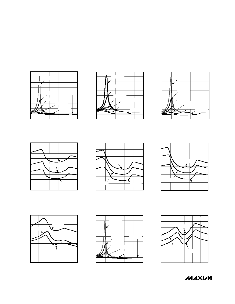
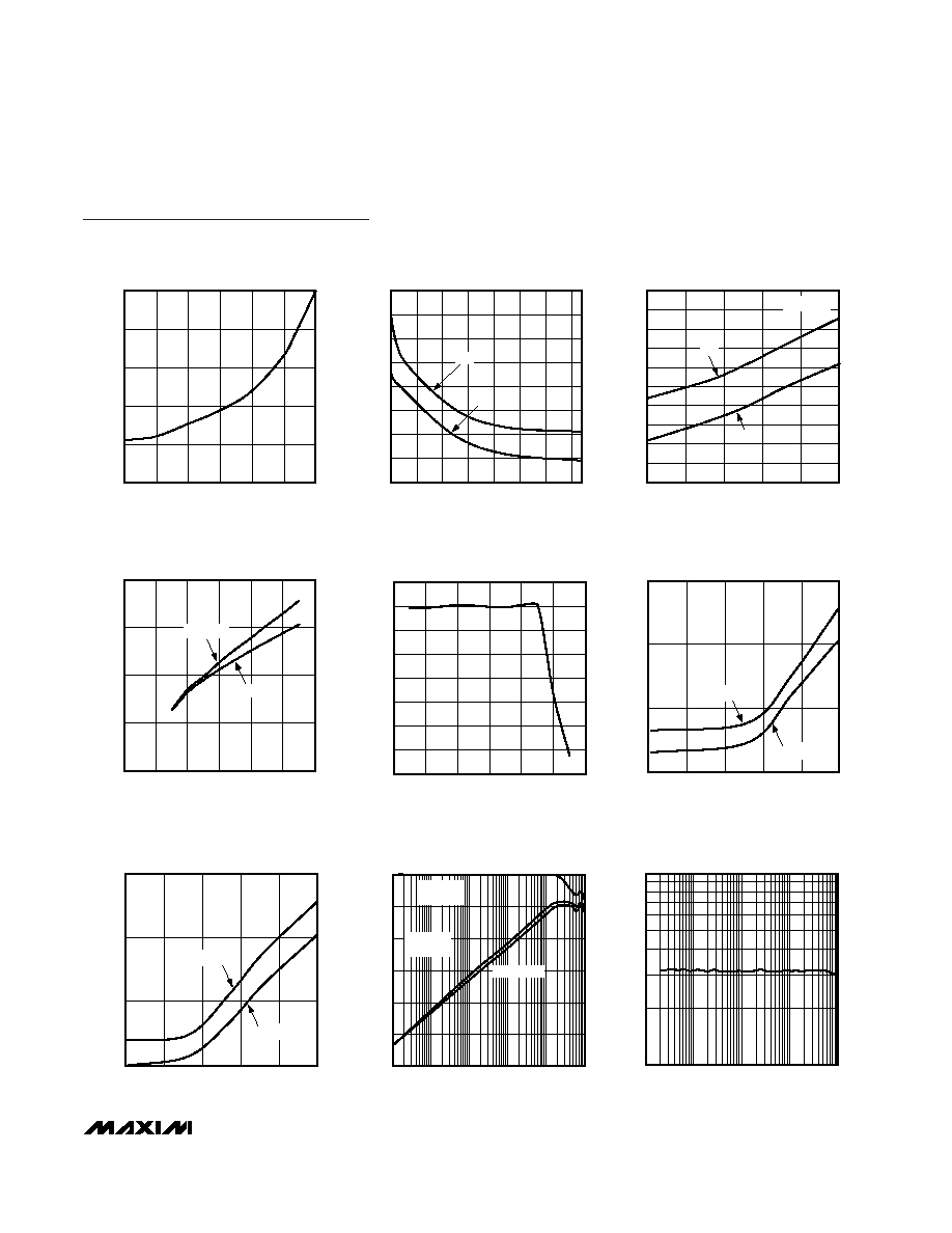
Typical Operating Characteristics
(T
A
= +25°C, unless otherwise noted.)
0
0.4
0.2
1.0
0.8
0.6
1.6
1.4
1.2
1.8
0
2
1
3
4
5
MAX4684
NC ON-RESISTANCE vs. COM VOLTAGE
MAX4684/5 toc01
V
COM
(V)
R
ON
(
)
V+ = +3.0V
V+ = +5.0V
V+ = +1.8V
V+ = +2.0V
V+ = +2.3V
V+ = +2.5V
NO ON-RESISTANCE vs. COM VOLTAGE
0
0.5
1.5
1.0
2.0
2.5
0
2
1
3
4
5
R
ON
(
)
MAX4684/5 toc03
V
COM
(V)
V+ = +5.0V
V+ = +1.8V
V+ = +2.0V
V+ = +2.3V
V+ = +2.5V
V+ = +3.0V
MAX4685
NC ON-RESISTANCE vs. COM VOLTAGE
0
0.2
0.4
0.6
0.8
1.2
1.4
1.8
1.0
1.6
2.0
0
2
1
3
4
5
R
ON
(
)
MAX4684/5 toc02
V
COM
(V)
V+ = +5.0V
V+ = +2.3V
V+ = +3.0V
V+ = +1.8V
V+ = +2.0V
V+ = +2.5V
0.10
0.12
0.14
0.16
0.20
0.18
0.22
0.24
0.26
0.28
0
2
1
3
4
5
MAX4684/5 toc04
MAX4684
NC ON-RESISTANCE vs. COM VOLTAGE
V
COM
(V)
R
ON
(
)
T
A
= +85°C
V+ = +5V
T
A
= -40°C
T
A
= +25°C
0.10
0.15
0.20
0.25
0.30
0.35
0.40
0
1
2
3
4
5
MAX4684/5 toc06
NO ON-RESISTANCE vs. COM VOLTAGE
V
COM
(V)
R
ON
(
)
T
A
= +85°C
V+ = +5V
T
A
= -40°C
T
A
= +25°C
0.10
0.15
0.20
0.25
0.30
0.35
0.40
0.45
0
1
2
3
4
5
MAX4684/5 toc05
MAX4685
NC ON-RESISTANCE vs. COM VOLTAGE
V
COM
(V)
R
ON
(
)
V+ = +5V
T
A
= +25°C
T
A
= -40°C
T
A
= +85°C
0
1.0
1.5
0.5
2.0
2.5
3.0
0.10
0.15
0.20
0.25
0.30
0.35
MAX4684/5 toc07
MAX4684
NC ON-RESISTANCE vs. COM VOLTAGE
V
COM
(V)
R
ON
(
)
V+ = +3V
T
A
= +85°C
T
A
= -40°C
T
A
= +25°C
0.15
0.10
0.20
0.25
0.30
0.35
0.40
0.45
0.50
0
1.0
0.5
1.5
2.0
2.5
3.0
MAX4684/5 toc09
NO ON-RESISTANCE vs. COM VOLTAGE
V
COM
(V)
R
ON
(
)
V+ = +3V
T
A
= +85°C
T
A
= +25°C
T
A
= -40°C
0
0.4
0.2
1.0
0.8
0.6
1.6
1.4
1.2
1.8
0
2
1
3
4
5
MAX4684
NC ON-RESISTANCE vs. COM VOLTAGE
MAX4684/5 toc01
V
COM
(V)
R
ON
(
)
V+ = +3.0V
V+ = +5.0V
V+ = +1.8V
V+ = +2.0V
V+ = +2.3V
V+ = +2.5V
MAX4684/MAX4685
0.5
/0.8
Low-Voltage, Dual SPDT
Analog Switches in UCSP
_______________________________________________________________________________________
5
0
20
60
40
80
100
0
2
1
3
4
5
6
SUPPLY CURRENT vs. SUPPLY VOLTAGE
MAX4684/5 toc10
V
SUPPLY
(V)
SUPPLY CURRENT (pA)
0
20
10
40
30
50
60
70
80
1.8
2.8
3.3
2.3
3.8
4.3
4.8
5.3
MAX4684/5 toc11
V
SUPPLY
(V)
t
ON
/t
OFF
(ns)
TURN-ON/TURN-0FF TIMES
vs. SUPPLY VOLTAGE
t
ON
t
OFF
0
15
10
5
20
25
30
35
40
45
50
-40
10
-15
35
60
85
MAX4684/5 toc12
TURN-ON/TURN-0FF TIMES
vs. TEMPERATURE
V+ = +3V
t
ON
/t
OFF
(ns)
TEMPERATURE (°C)
t
ON
t
OFF
2.0
1.5
1.0
0.5
0
0
3
1
2
4
5
6
LOGIC THRESHOLD VOLTAGE
vs. SUPPLY VOLTAGE
MAX4684/5 toc13
LOGIC THRESHOLD VOLTAGE (V)
V
SUPPLY
(V)
V
IN
RISING
V
IN
FALLING
-500
-400
-300
-200
-100
0
100
200
300
0
2
1
3
4
5
6
CHARGE INJECTION vs. COM VOLTAGE
MAX4684/5 toc14
Q (pC)
V
COM
(V)
-40
10
-15
35
60
85
MAX4684/5 toc15
TEMPERATURE (°C)
ON/OFF-LEAKAGE CURRENT (pA)
1
10
100
1000
MAX4684
ON/OFF-LEAKAGE CURRENT
vs. TEMPERATURE
I
COM(ON)
I
COM(OFF)
-40
10
-15
35
60
85
MAX4684/5 toc16
TEMPERATURE (°C)
ON/OFF-LEAKAGE CURRENT (pA)
1
10
100
1000
MAX4685
ON/OFF-LEAKAGE CURRENT
vs. TEMPERATURE
I
COM(ON)
I
COM(OFF)
FREQUENCY RESPONSE (µMAX)
FREQUENCY (MHz)
0.001
1
10
100
0.01
0.1
LOSS (dB)
-120
-100
-80
-20
-40
-60
0
MAX4684/85 toc17
ON-
RESPONSE
OFF-
ISOLATION
CROSSTALK
10
100
1k
10k
100k
TOTAL HARMONIC DISTORTION
PLUS NOISE vs. FREQUENCY
MAX4684/5 toc18
FREQUENCY (Hz)
THD + N (%)
0.01
0.1
Typical Operating Characteristics (continued)
(T
A
= +25°C, unless otherwise noted.)