MAX4610/MAX4611/MAX4612
Low-Voltage, Quad, SPST
CMOS Analog Switches
________________________________________________________________ Maxim Integrated Products
1
19-4793; Rev 2; 11/03
For pricing, delivery, and ordering information, please contact Maxim/Dallas Direct! at
1-888-629-4642, or visit Maxim's website at www.maxim-ic.com.
General Description
The MAX4610/MAX4611/MAX4612 are quad, low-volt-
age, single-pole/single-throw (SPST) analog switches.
On-resistance (100
, max) is matched between switch-
es to 4
, max and is flat (4, max) over the specified
signal range. Each switch handles V+ to GND analog
signal levels. Maximum off-leakage current is only 1nA
at T
A
= +25°C and 2nA at T
A
= +85°C.
The MAX4610 has four normally open (NO) switches,
and the MAX4611 has four normally closed (NC)
switches. The MAX4612 has two NO switches and two
NC switches. These CMOS switches operate from a
single +2V to +12V supply. All digital inputs have +0.8V
and +2.4V logic thresholds, ensuring TTL/CMOS-logic
compatibility when using a single +5V supply.
________________________Applications
Battery-Operated Equipment
Audio/Video Signal Routing
Low-Voltage Data-Acquisition Systems
Sample-and-Hold Circuits
Communication Circuits
____________________________Features
o Offered in Automotive Temperature Range
(-40°C to +125°C)
o Guaranteed On-Resistance
100
max (5V Supply)
46
max (12V Supply)
o Guaranteed Match Between Channels (4, max)
o Guaranteed Flatness Over Signal Range (18, max)
o Off-Leakage Current Over Temperature
<2nA at T
A
= +85°C
o >2kV ESD Protection per Method 3015.7
o Rail-to-Rail
®
Signal Handling
o TTL/CMOS-Logic Compatible
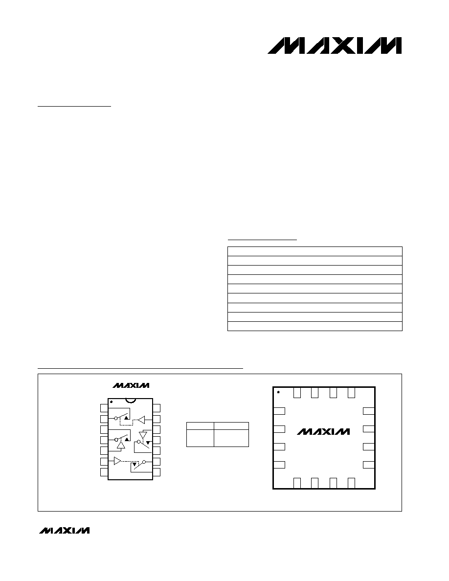
14
13
12
11
10
9
8
1
2
3
4
5
6
7
MAX4610
TSSOP/SO/DIP
V+
IN1
IN4
NO4
COM4
COM3
NO3
COM2
NO2
COM1
NO1
GND
IN3
IN2
TOP VIEW
INPUT
SWITCH STATE
LOW
HIGH
OFF
ON
16
V+
15
N.C.
14
IN1
13
IN4
5
IN2
6
IN3
7
GND
8
NO3
MAX4610
2
COM1
1
NO1
3
NO2
4
COM2
11
NO4
12
N.C.
10
COM4
9
COM3
QFN
Pin Configurations/Truth Tables
Ordering Information
Ordering Information continued at end of data sheet.
*Contact factory for dice specifications.
Rail-to-Rail is a registered trademark of Nippon Motorola, Ltd.
MAX4611/MAX4612 Pin Configurations/Truth Tables appear at end of data sheet.
14 Plastic DIP
-40°C to +125°C
MAX4610EPD
14 TSSOP
-40°C to +85°C
MAX4610EUD
14 Narrow SO
-40°C to +85°C
MAX4610ESD
16 QFN
-40°C to +85°C
MAX4610EGE
Dice*
14 Plastic DIP
0°C to +70°C
0°C to +70°C
MAX4610C/D
MAX4610CPD
14 Narrow SO
14 TSSOP
PIN-PACKAGE
TEMP RANGE
0°C to +70°C
0°C to +70°C
MAX4610CSD
MAX4610CUD
PART
MAX4610/MAX4611/MAX4612
Low-Voltage, Quad, SPST
CMOS Analog Switches
2
_______________________________________________________________________________________
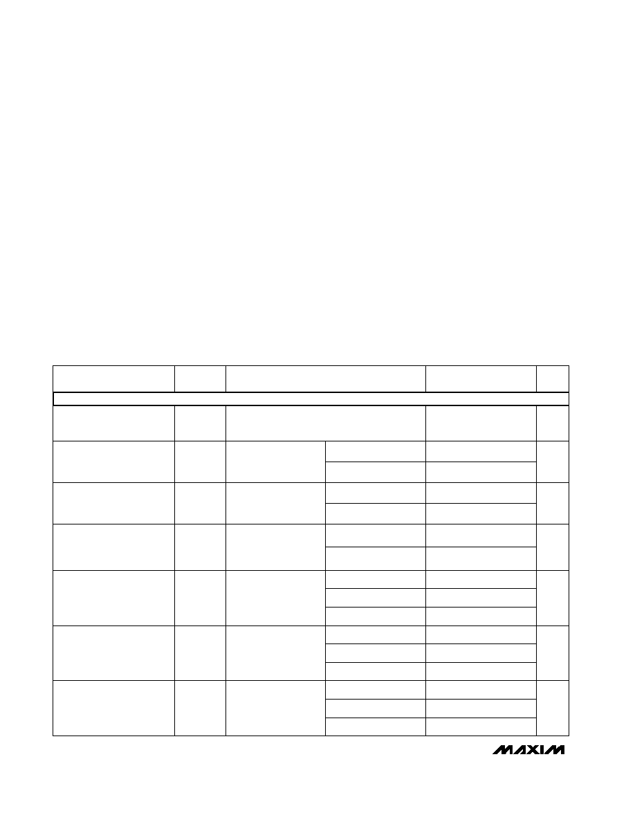
ABSOLUTE MAXIMUM RATINGS
ELECTRICAL CHARACTERISTICS--Single +5V Supply
(V+ = +5V ±10%, V
IN_H
= 2.4V, V
IN_L
= 0.8V, T
A
= T
MIN
to T
MAX
, unless otherwise noted.)
Stresses beyond those listed under "Absolute Maximum Ratings" may cause permanent damage to the device. These are stress ratings only, and functional
operation of the device at these or any other conditions beyond those indicated in the operational sections of the specifications is not implied. Exposure to
absolute maximum rating conditions for extended periods may affect device reliability.
(Voltages referenced to GND)
V+ ...........................................................................-0.3V to +13V
IN_, COM_, NO_, NC_ (Note 1)....................-0.3V to (V + +0.3V)
Continuous Current (any terminal)
(pulsed at 1ms, 10% duty cycle) .....................................20mA
Peak Current (any terminal)
(pulsed at 1ms, 10% duty cycle) .....................................40mA
ESD per Method 3015.7.......................................................>2kV
Continuous Power Dissipation (T
A
= +70°C)
14-Pin TSSOP (derate 6.3mW/°C above +70°C) ..........500mW
14-Pin Narrow SO (derate 8.00mW/°C above +70°C) ..640mW
14-Pin Plastic DIP (derate 10.00mW/°C above +70°C) ..800mW
16-Pin QFN (derate 18.5mW/°C above +70°C) ..........1481mW
Operating Temperature Ranges
MAX461_C_ _ ......................................................0°C to +70°C
MAX461_E_ _....................................................-40°C to +85°C
MAX461_A_ _ .................................................-40°C to +125°C
Storage Temperature Range .............................-65°C to +160°C
Lead Temperature (soldering, 10s) .................................+300°C
V+ = 5.5V;
V
COM
_ = 1V, 4.5V;
V
NO
= 4.5V, 1V
V+ = 4.5V,
I
COM
_ = 1mA,
V
NO
_ = V
NC
_= 3V
V+ = 4.5V;
I
COM
_ = 1mA;
V
NO
_ = V
NC
_= 3V,
2V, 1V
CONDITIONS
nA
I
NO(OFF)
NO or NC Off-Leakage
Current (Note 6)
-30
30
-0.1
0.1
25
R
FLAT(ON)
On-Resistance Flatness
(Note 5)
V
0
V+
V
COM
_,
V
NO
_
,
V
NC
_
Analog Signal Range
(Note 3)
12
18
R
ON
On-Resistance Match
Between Channels (Note 4)
1.0
4
70
100
UNITS
MIN
TYP
MAX
(Note 2)
SYMBOL
PARAMETER
T
A
= +25°C
T
A
= +25°C
T
A
= +25°C
T
A
= T
MIN
to T
MAX
T
A
= +25°C
T
A
= -40°C to +125°C
V+ = 5.5V;
V
COM
_ = 1V, 4.5V;
V
NO
_ = V
NC
_= 4.5V, 1V
T
A
= +25°C
nA
I
COM(OFF)
COM Off-Leakage Current
(Note 6)
-30
30
T
A
= -40°C to +125°C
-0.1
0.1
V+ = 5.5V;
V
COM
= 1V, 4.5V;
V
NO
_ = V
NC
_= 1V, 4.5V,
or floating
nA
I
COM(ON)
COM On-Leakage Current
(Note 6)
T
A
= +25°C
-0.2
0.2
On-Resistance
R
ON
V+ = 4.5V,
I
COM
_ = 1mA,
V
NO
_ = V
NC
_= 3V
Note 1: Signals on NO_, NC_, COM_, or IN_ exceeding V+ or GND are clamped by internal diodes. Limit forward-diode current to
maximum current rating.
T
A
= T
MIN
to T
MAX
8
150
T
A
= T
MIN
to T
MAX
-30
30
T
A
= -40°C to +125°C
-4
4
T
A
= -40°C to +85°C
-2
2
T
A
= -40°C to +85°C
-2
2
T
A
= -40°C to +85°C
ANALOG SWITCH

MAX4610/MAX4611/MAX4612
Low-Voltage, Quad, SPST
CMOS Analog Switches
_______________________________________________________________________________________
3
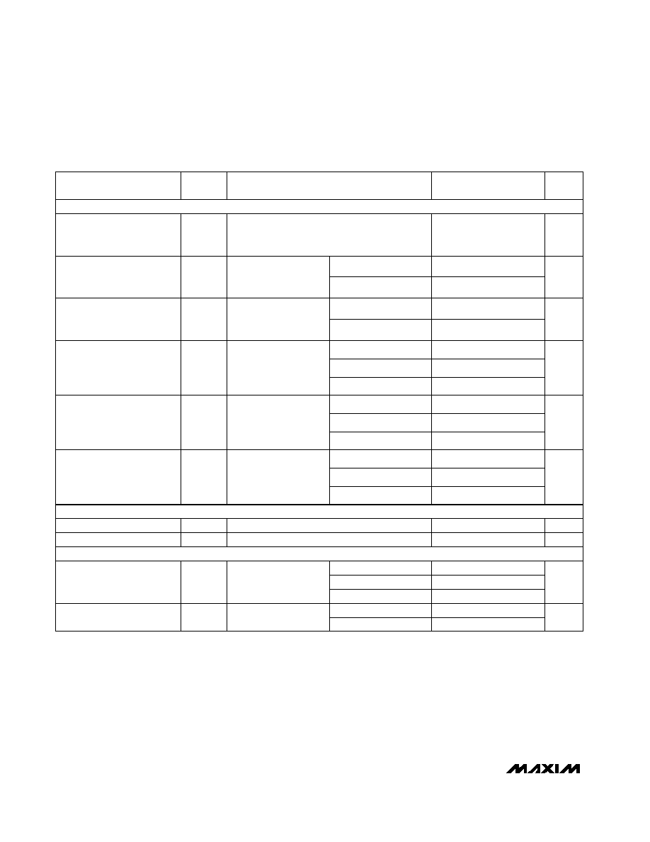
ELECTRICAL CHARACTERISTICS--Single +5V Supply (continued)
(V+ = +5V ±10%, V
IN_H
= 2.4V, V
IN_L
= 0.8V, T
A
= T
MIN
to T
MAX
, unless otherwise noted.)
PARAMETER
SYMBOL
MIN
TYP
MAX
(Note 2)
UNITS
Input Current with Input
Voltage High
I
IN_H
-0.1
0.001
0.1
µA
CONDITIONS
V
IN
_ = 2.4V, all others = 0.8V
Input Current with Input
Voltage Low
I
IN_L
-0.1
0.001
0.1
µA
V
IN
_ = 0.8V, all others = 2.4V
Turn-On Time
t
ON
35
60
ns
Charge Injection
V
CTE
1
5
pC
C
L
= 1.0nF, V
GEN
= 0,
R
GEN
= 0, Figure 3
T
A
= +25°C
T
A
= T
MIN
to T
MAX
80
V
COM
_ = 3V, Figure 2
T
A
= +25°C
T
A
= T
MIN
to T
MAX
30
V
COM
_ = 3V, Figure 2
Turn-Off Time
t
OFF
15
20
ns
Power-Supply Range
Signal = 0dBm, Figure 4,
50
in and out
On-Channel Bandwidth
BW
300
MHz
T
A
= +25°C
T
A
= +25°C
R
L
= 50
, C
L
= 5pF,
f = 1MHz, Figure 4
Off-Isolation (Note 7)
V
ISO
-60
dB
T
A
= +25°C
R
L
= 50
, C
L
= 5pF,
f = 1MHz, Figure 5
Crosstalk (Note 8)
V
CT
-80
dB
T
A
= +25°C
f = 1MHz, Figure 6
NO_ or NC_ Capacitance
C
(OFF)
16
pF
T
A
= +25°C
f = 1MHz, Figure 6
COM_ Off-Capacitance C
COM(OFF)
16
pF
T
A
= +25°C
f = 1MHz, Figure 6
COM_ On-Capacitance
C
COM(ON)
pF
2
12
V
Supply Current
23
I+
V
IN
= 0 or V+,
all switches on or off
-1
0.001
1
µA
T
A
= +25°C
T
A
= +25°C
600
IN and OUT,
20Hz to 20kHz, 2Vp-p
Total Harmonic
Distortion
THD
%
0.009
Input High Voltage
V
IN_H
2.4
1.5
V
Input Low Voltage
V
IN_L
1.4
0.8
V
LOGIC INPUT
SUPPLY
DYNAMIC (Note 3)
MAX4610/MAX4611/MAX4612
Low-Voltage, Quad, SPST
CMOS Analog Switches
4
_______________________________________________________________________________________
ELECTRICAL CHARACTERISTICS--Single +3V Supply
(V+ = +3V, V
IN_H
= 2.4V, V
IN_L
= 0.5V, T
A
= T
MIN
to T
MAX
, unless otherwise noted.)
PARAMETER
Analog Signal Range
(Note 3)
SYMBOL
V
COM
_,
V
NO
_,
V
NC
_
CONDITIONS
MIN
TYP
MAX
(Note 2)
0
V+
UNITS
V
On-Resistance
R
ON
V+ = 2.7V,
I
COM
_ = 1mA,
V
NO
_ = V
NC
_ = 1V
175
360
-0.1
0.1
-2
2
NO_ or NC_ Off-Leakage
Current (Notes 3, 6)
I
NO(OFF)
V+ = 3.6V,
V
COM
_ = 0.5V, 3V;
V
NO
_ = V
NC
_ = 3V,
0.5V
-30
30
nA
-0.2
0.2
T
A
= +25°C
T
A
= T
MIN
to T
MAX
450
On-Resistance Match
Between Channels (Note 4)
R
ON
V+ = 2.7V,
I
COM
_ = 1mA,
V
NO
_ = V
NC
_ = 1V
2
5
T
A
= +25°C
T
A
= T
MIN
to T
MAX
10
T
A
= +25°C
T
A
= -40°C to + 85°C
T
A
= -40°C to + 125°C
-4
4
COM_On-Leakage Current
(Notes 3, 6)
I
COM(ON)
V+ = 3.6V,
V
COM
_ = 0.5V, 3V;
V
NO
_ = V
NC
_ = 0.5V,
3V, or floating
-30
30
nA
Input High Voltage
V
IN_H
2.4
1.0
V
Input Low Voltage
V
IN_L
1.0
0.5
V
T
A
=+25°C
T
A
= -40°C to + 85°C
-0.1
0.1
T
A
= -40°C to + 125°C
-2
2
COM_ Off-Leakage Current
(Notes 3, 6)
I
COM(OFF)
V+ = 3.6V,
V
COM
_ = 0.5V, 3V;
V
NO
_ = V
NC
_ = 3V,
0.5V
-30
30
nA
T
A
= +25°C
T
A
= -40°C to +85°C
50
90
120
Turn-On Time
t
ON
V
COM
_ = 1.5V,
Figure 2
140
ns
30
45
Turn-Off Time
t
OFF
V
COM
_ = 1.5V,
Figure 2
60
ns
T
A
= +25°C
T
A
= -40°C to +85°C
T
A
= -40°C to +125°C
T
A
= -40°C to +125°C
T
A
= +25°C
T
A
= T
MIN
to T
MAX
ANALOG SWITCH
LOGIC INPUTS
DYNAMIC (Note 3)
MAX4610/MAX4611/MAX4612
Low-Voltage, Quad, SPST
CMOS Analog Switches
_______________________________________________________________________________________
5
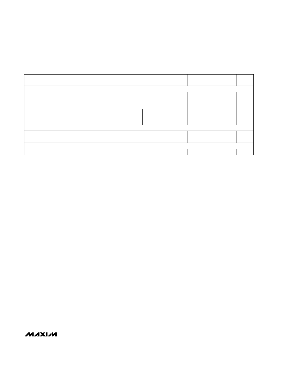
PARAMETER
SYMBOL
MIN
TYP
MAX
(Note 2)
UNITS
Analog Signal Range
(Note 3)
V
COM
_,
V
NO
_,
V
NC
_,
0
V+
V
CONDITIONS
On-Resistance
R
ON
30
45
V+ = 12V,
I
COM
= 2mA,
V
NO_
= V
NC
_ = 10V
T
A
= +25°C
T
A
= T
MIN
to T
MAX
60
Note 2: The algebraic convention, where the most negative value is a minimum and the most positive value a maximum, is used in
this data sheet.
Note 3: Guaranteed by design.
Note 4:
R
ON
= R
ON
(max) - R
ON
(min).
Note 5: Flatness is defined as the difference between the maximum and minimum value of on-resistance as measured over the
specified analog signal range.
Note 6: Leakage parameters are 100% tested at maximum-rated hot temperature and guaranteed by correlation at +25°C.
Note 7: Off-Isolation = 20log
10
(V
COM_
/ V
NO_
), V
COM_
= output, V
NO_
= input to off switch.
Note 8: Between any two switches.
ELECTRICAL CHARACTERISTICS--Single +12V Supply
(V+ = +12V, V
IN_H
= 4V, V
IN_L
= 0.8V, T
A
= T
MIN
to T
MAX
, unless otherwise noted.)
Input High Voltage
V
IN_H
4.0
2.8
V
Input Low Voltage
V
IN_L
2.5
0.8
V
Positive Supply Current
I+
-1
0.001
1
µA
V
IN_
= 0 or V+, all switches on or off
ANALOG SWITCH
LOGIC INPUTS
SUPPLY