MAX445
Low-Cost, High-Resolution, 200MHz
Video CRT Driver
________________________________________________________________
Maxim Integrated Products
1
24
23
22
21
20
19
18
17
1
2
3
4
5
6
7
8
CONTRAST
OFFSET
VREF
GND
TOP VIEW
V
EE
VIN+
VIN-
GNDA
16
15
14
13
9
10
11
12
GND
BLANK
V
CC
V
EE
V
EEO
GND
GND
GND
VCB
N.C.
IOUT
N.C.
GND
GND
GND
VCB
MAX445
Power-Tab DIP
IOUT
OFFSET
CONTRAST
BLANK
V
AA
R
L
V
OUT
PRE-AMP
VCB
VIN-
VIN+
CURRENT
AMP
VREF
BAND
GAP
GNDA
GND
MAX445
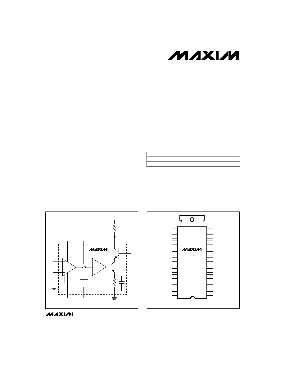
__________________Pin Configuration
________________Functional Diagram
Call toll free 1-800-998-8800 for free samples or literature.
_______________General Description
The MAX445 is a high-performance, monolithic, variable-
gain transconductance amplifier with a high-voltage
open-collector output capable of directly driving a video
display (CRT cathode). A 2.5ns rise time is achieved
using a peaking network with a 200
load resistor and
an 8pF total load (CRT and parasitic capacitance).
Differential inputs and a linear adjustable gain stage
with an output offset adjustment make the versatile
MAX445 well suited for many video display applica-
tions. A buffered bandgap reference voltage is avail-
able for the gain (contrast) and offset adjustments
along with a TTL BLANK input to turn off the output cur-
rent, independent of signal input.
The MAX445 is available in a 24-pin power-tab DIP
package. A suitable heatsink must be attached to
maintain the junction temperature within the recom-
mended operating range.
________________________Applications
CRT Driver for High-Resolution Monochrome and
Color Displays
High-Voltage, Variable-Gain Transconductance
Amplifier
____________________________Features
o
2.5ns Rise/Fall Time into an 8pF Load
o
200MHz Small-Signal Bandwidth
o
50Vp-p Output
o
Ground Referenced Differential Inputs
o
Linear Variable Gain for Contrast Control
o
Offset Adjustment for Black Level
o
5.5V Bandgap Reference
o
Drives 1280 x 1024 and 1530 x 1280 Displays
______________Ordering Information
PART
MAX445CPG
MAX445C/D
0�C to +70�C**
0�C to +70�C*
TEMP. RANGE
PIN-PACKAGE
24 Power-Tab DIP
Dice
* Case temperature range, T
CASE
= 0�C to +90�C. See Absolute
Maximum Ratings and Applications Information for thermal/heat
sink considerations.
**Dice are specified at T
J
= +25�C, DC parameters only.
19-0302; Rev 0; 9/94

MAX445
Low-Cost, High-Resolution, 200MHz
Video CRT Driver
2
_______________________________________________________________________________________
ABSOLUTE MAXIMUM RATINGS
ELECTRICAL CHARACTERISTICS
(V
AA
= 20V, VCB = 10V �0.5V, V
CC
= 10V �0.5V, V
EE
= -10.5V �0.5V, VIN = (VIN+) - (VIN-) = 0V, CONTRAST = 1.0V,
OFFSET = 1.0V, R
L
= 0
, BLANK = 0.4V, T
CASE
= +25�C, unless otherwise noted.)
Stresses beyond those listed under "Absolute Maximum Ratings" may cause permanent damage to the device. These are stress ratings only, and functional
operation of the device at these or any other conditions beyond those indicated in the operational sections of the specifications is not implied. Exposure to
absolute maximum rating conditions for extended periods may affect device reliability.
V
AA
Output Supply.................................................................80V
V
AA
Output Supply with Respect to VCB...............................70V
VCB Common-Base Supply ...................................................20V
V
CC
Positive Supply ............................................................12.5V
V
EE
Negative Supply..........................................................-12.5V
Differential Input Voltage..........................................................2V
Common-Mode Input Voltage................................................�2V
Contrast Input Voltage.................................................-1V to +6V
Offset Input Voltage.....................................................-1V to +6V
Blank Input Voltage .....................................................-1V to +6V
Bandgap-Reference Output Current ...................................-5mA
Continuous Power Dissipation
derate at 170mW/�C above T
CASE
= +90�C .......................10W
Operating Junction Temperature ......................-55�C to +150�C
Storage Temperature.........................................-55�C to +150�C
Lead Temperature (soldering, 10sec) .............................+300�C
OFFSET = 0V, R
LOAD
= 100
VIN = 0.2V, OFFSET = 0V
CONTRAST = 4.0V, OFFSET = 1.0V
I
VEE
+ I
VEEO
CONTRAST = 0V
CONTRAST = 1.0V
CONTRAST = 5.0V
BLANK = 2.4V, CONTRAST = 5.0V,
VIN- = 0.3V
CONTRAST = 0V to 5V
T
C
= +25�C to +90�C
V
CM
= �0.5V, CONTRAST = 5.0V
BLANK = 2.4V, OFFSET = 3V
BLANK = 2.4V, OFFSET = 1V, V
AA
= 75V
OFFSET = 1.0V
V
CC
, V
EE
= �5%, VIN = +250mV,
CONTRAST = 5.0V, referred to input
BLANK = 0.4V
BLANK = 2.4V
I
LOAD
= 2mA
CONTRAST = 5.0V
CONDITIONS
MHz
200
BW
Bandwidth, 3dB
%
�3
Contrast Linearity Error (
Gm/
Contrast)
%
�2
Amplifier Linearity Error (
Gm/
V
IN
)
-25
25
70
120
mA/V
400
600
Gm
Transconductance, I
OUT
to VIN
mA
�1
I
OUT
Output Current Change vs. VIN, Blanked
mA
�10
I
OUT
Output Current Change vs. Contrast ADJ
mA
�3
I
OUT
Output Current Change vs. Temperature
�1
mA
�1
I
OUT
Output Current (Blanked)
V
5.25
5.75
V
REF
Reference Output Voltage
pF
2
C
IN
VIN+ or VIN- Input Capacitance
mA
-100
I
EE
Negative Supply Current
mA
70
I
CC
mA
40
I
CB
Output-Common-Base Supply Current
Positive Supply Current
k
10
R
VIN
VIN+ or VIN- DC Input Impedance
dB
36
CMRR
Input Common-Mode Rejection Ratio
�A
-50
50
IIS
VIN+ or VIN- Signal Input Current
�A
0
10
IIB
Offset Input Bias Current
dB
25
PSRR
Power-Supply Rejection Ratio
mA
-0.6
0
I
IL
Low Blank Input Bias Current
mA
-0.4
0
IIH
High Blank Input Bias Current
�A
0
10
IIC
Contrast Input Bias Current
UNITS
MIN
TYP
MAX
SYMBOL
PARAMETER
OFFSET = 5.0V, CONTRAST = 1V
OFFSET = 0V, CONTRAST = 4.0V
80
140
mA
-0.1
25
I
OUT
Output Current
MAX445
Low-Cost, High-Resolution, 200MHz
Video CRT Driver
_______________________________________________________________________________________
3
ELECTRICAL CHARACTERISTICS (continued)
(V
AA
= 20V, VCB = 10V �0.5V, V
CC
= 10V �0.5V, V
EE
= -10.5V �0.5V, VIN = (VIN+) - (VIN-) = 0V, CONTRAST = 1.0V,
OFFSET = 1.0V, R
L
= 0
, BLANK = 0.4V, T
CASE
= +25�C, unless otherwise noted.)
CONDITIONS
C
L
= 8pF, no peaking
R
L
= 200
,
C
L
= 8pF,
V
AA
= 75V,
t
r
(VIN) < 1ns,
ns
8
t
s
UNITS
MIN
TYP
MAX
SYMBOL
PARAMETER
Settling Time (90% to 100% �2%)
2.5
No peaking,
OUTp-p = 50V
With peaking,
OUTp-p = 45V
ns
3.6
t
r
, t
f
Rise/Fall Time (10% to 90%)
%
�2
Thermal Distortion
______________________________________________________________Pin Description
NAME
FUNCTION
1, 12, 13, 14,
15, 22, 23, 24
GND
High-Current Ground. Connect all pins to ground plane.
2
VREF
Reference Output (+5.5V)
PIN
3
OFFSET
Output Voltage Offset-Adjustment Input
4
CONTRAST
Output Gain-Adjustment Input
8, 9
V
EE
Negative Supply (-10.5V)
7
VIN+
Noninverting Signal Input
6
VIN-
Inverting Signal Input
5
GNDA
Pre-Amp Ground
19
IOUT
Open-Collector Current Output
18, 20
N.C.
No Connection--leave open
16, 17
VCB
Output Common-Base Supply (+10V)
11
BLANK
Blanking Input, TTL
10
V
CC
Positive Supply (+10V)
21
V
EEO
Negative Supply for Output Stage (-10.5V)
MAX445
Low-Cost, High-Resolution, 200MHz
Video CRT Driver
4
_______________________________________________________________________________________
__________Applications Information
Differential Inputs
VIN+ and VIN- are differential video input pins designed
to allow DC coupling of a 0V to +1V signal into VIN+, with
respect to VIN-. For correct operation, it is recommend-
ed that the signals applied to these inputs be kept within
�1V, with respect to ground. Although large signals and
offsets can be handled safely without damage, exceed-
ing these limits may cause output linearity to suffer.
Contrast Control
The contrast control is the overall DC-gain control that
will vary the voltage gain from 0V/V to -90V/V (with a
200
load resistor). An internal reference supply pin,
VREF, provides the nominal 5.5V needed to drive the
contrast input. Normally, a 5k
potentiometer between
VREF and ground is used to vary the contrast, but an
external source can be used instead of VREF, with some
degradation of gain stability with temperature.
The contrast control is a linear relationship. Vary the
input from 0V to 5V to achieve a voltage-gain range of
0V/V to -90V/V. This yields the following relationship for
overall voltage gain of this device (for IOUT < 250mA):
V
AA
- V
O
=
[V
IN
(Gm) + V
OFFSET
(0.02)] (R
L
)
V
AA
- V
O
= [V
IN
(V
CONTRAST
) (0.09) + V
OFFSET
(0.02)] (R
L
)
The MAX445's overall gain can vary by �20% due to
normal process variations of internal components. Also,
if multiple devices are used in a system, all devices
must track thermally (i.e., a common heatsink).
Offset Control
The offset control is used to set the output quiescent
current from 5mA to 110mA (typ) when the control input
is adjusted from 0V to 5V. Normally, offset is adjusted
using a 5k
potentiometer between VREF and ground.
Blank Control
When asserted (BLANK = TTL high), this input will dis-
able the video signal and allow the output to rise to the
V
AA
supply independent of offset control.
Bandgap Reference
VREF is a bandgap bias reference for easy adjustment
of the offset and contrast inputs. This reference has a
nominal output voltage of 5.5V �5% that can source up
to 4mA.
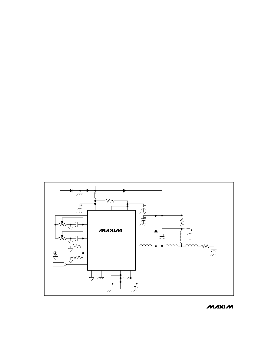
MAX445
0.1
�
F
3
V
EE
(-10.5V)
5k
+10V
D1
1N4152
50V
25
24
50
0.1
�
F
0.1
�
F
4
IOUT
D4
7
CONTRAST
VIN+
OFFSET
5k
-10.5V
ANALOG
INPUT
BLANK
GNDA
GND
2
10
17
16
VREF
6
VIN-
11
5
24*
BLANK
V
EE
BEAD*
V
EE
8
9
V
EEO
21
0.1
�
F
0.1
�
F
BEAD*
10pF
19
L2
NOTES:
C
L
COMBINES CRT CATHODE, AND PARASITIC C.
D4 (PHILIPS BAV20 OR HITACHI 1SS91) IS ARC PROTECTION DIODE.
SEE
APPLICATIONS INFORMATION SECTION.
L1, L2, L3, AND CB ARE
ELEMENTS OF THE PEAKING COIL.
L
S
IS THE TOTAL INDUCTANCE
TO THE CATHODE. R
S
IS A SERIES
ARC PROTECTION ELEMENT.
L3
L1
L
S
R
L
200
10W
R
S
100
W (CARBON)
D2
1N4152
50V
D3
1N486A
100V
22
�
F
100V
CB
V
AA
(+75V)
C
R
1
2
C
L
V
CC
VCB
VCB
* STACK POLE 57-0180 OR
INDIANA GENERAL F-1650-H
Figure 1. Typical Connection Diagram

IOUT
The MAX445's output is an open collector of a cascode
amplifier. This output is designed to work with nominal
output supplies of V
AA
= +75V. The high-voltage supply
must be greater than any applied VCB voltage for proper
operation. The MAX445 sinks up to 250mA. Optimum
performance into a capacitive load can be achieved
when an impedance-matching network is used.
VCB
The output stage consists of a common-base, high-voltage
stage and a high-speed, low-voltage current amplifier in a
cascode arrangement. The VCB input is the base connec-
tion to the common-base device of this stage. Be sure to
provide a stable DC voltage at this pin of nominally +10V.
High-frequency compensation at this input is required to
avoid output oscillations. Use a series 24
resistor to sup-
ply, shunted with a 10pF capacitor to ground (Figure 1).
Smaller values of this RC combination will improve output
rise/fall times, but can cause output oscillations.
Power Supplies
+10V and -10.5V supplies are required for proper opera-
tion. These supplies can be set to �12V for conve-
nience, however this will add additional component
power dissipation. The high-voltage supply, V
AA
, can be
any voltage between VCB + 10V and VCB + 65V.
V
EEO
(pin 21) is the negative supply to the output stage
and must be DC connected to V
EE
(pins 8 and 9), the
most negative voltage applied to the device. However,
V
EEO
must be decoupled from V
EE
to prevent output
oscillations. A ferrite bead and separate 0.1�F decou-
pling capacitors, as shown in Figure 1, will provide
appropriate decoupling.
Power-Supply Sequencing
Power-supply sequencing is important to avoid internal
device latchup. To avoid sequencing problems, external
diodes should be placed from V
EE
to ground, from
ground to V
CC
, and from V
CC
to the output supply (V
AA
),
as shown in Figure 1. With diodes used as shown, spe-
cial power-supply sequencing is not required.
CRT Arc Protection
The MAX445 must be protected from electrostatic dis-
charge ("arcs") from the CRT. It is recommended that the
output be clamped with a low-capacitance (less than
2pF) diode to the V
AA
supply. The peak current-handling
capability required of the diode is a function of the CRT
arc characteristics, but typically should be 1A or more,
such as Philips BAV20 or Hitachi 1SS91. For additional
information regarding arc protection, contact Maxim's
applications department.
Impedance Matching Network
For maximum speed from the MAX445, be sure to
"match" the output to the CRT. Figure 1's typical connec-
tion diagram shows a network (including parasitic reac-
tances) associated with arc protection devices, CRT
wiring and grid structure, and load resistors. These para-
sitic reactances are all detrimental to good transient
response and should be minimized as much as possible.
C
L
is the grid-to-cathode capacitance of the CRT, plus
any parasitic capacitance to ground associated with the
cathode structure. This capacitance varies from tube-
type to tube-type over the 4pF to 12pF range.
In Figure 1, L
S
is the inductance of the lead from the
amplifier board to the CRT cathode and the return path
from the grid to circuit ground. A wire in free space has
an inductance of 20nH/inch to 25nH/inch. With care, the
total path through the CRT gun can be kept at 1.5 to 2
inches, such that L
S
ranges from 30nH to 50nH.
Excessive lead length will cause undesirable overshoot
and ringing in the transient response.
The peaking networks assume that 2pF of parasitic
capacitance is associated with the CRT arc protection
diode connected at the junction of L3 and L1.
Lr is the parasitic inductance of the load resistor, R
L
. In
some cases, C
R
may be needed to improve step
response.
R
S
is a damping resistor in series with the CRT grid.
It also provides current limiting in the event of CRT
arcing.
The equations for determining optimum peaking net-
work values are as follows:
L1 = (R
L
)
2
(C
L
) / 4
L2 = 3(R
L
)
2
(C
L
) / 4
C
B
= C
L
/ 5
R
S
= R
L
/ 2
L3 = k
3
(R
L
)
2
[2.5 x 10
-12
]
C
R
(optional) = Lr / (2R
L2
)
k
3
is an empirically determined factor increasing with
C
L
and varying from 0 for C
L
~ 2pF to 1 for C
L
~ 12pF.
However, L3 >100nH will compromise large-signal per-
formance.
Table 1 shows peaking networks for the nominal load,
R
L
= 200
(and R
S
= 100
).
Optimum peaking depends on board layout and CRT
construction. The values given by these equations
should be used as starting points for empirically deter-
mining optimum values.
MAX445
Low-Cost, High-Resolution, 200MHz
Video CRT Driver
_______________________________________________________________________________________
5