General Description
The MAX4447/MAX4448/MAX4449 single-ended-to-
differential line drivers are designed for high-speed
communications. Using current feedback for greater
bandwidth, these devices deliver full-power bandwidths
up to 405MHz and feature slew rates as high as
6500V/µs. The MAX4447 has a fixed gain of +2V/V and
a small-signal bandwidth of 430MHz. The MAX4448/
MAX4449 have small-signal bandwidths of 330MHz
and 400MHz, respectively, and are internally compen-
sated for minimum gain configurations of +2V/V and
+5V/V, respectively. For greater design flexibility, the
MAX4448/MAX4449 allow for variable gain selection
using external gain-setting resistors. A low-power
enable mode reduces current consumption below 5.5mA
and places the outputs in a high-impedance state.
The MAX4447/MAX4448/MAX4449 can deliver differen-
tial output swings of ±6.2V from ±5V supplies with a
50
load. Excellent differential gain/phase and noise
specifications make these amplifiers ideal for a wide
variety of video and RF signal-processing and transmis-
sion applications.
Applications
Differential Line Driver
Single-Ended-to-Differential Conversion
High-Speed Differential Transmitter
Coaxial to Twisted-Pair Converter
Differential Pulse Amplifier
Differential ADC Driver
xDSL Applications
Video and RF Signal Processing and Transmission
Features
o 6500V/µs Slew Rate (MAX4449)
o Small-Signal Bandwidth
430MHz (MAX4447)
330MHz (MAX4448)
400MHz (MAX4449)
o 200MHz 0.1dB Gain Flatness (MAX4447)
o 130mA Output Drive Current
o +2V/V Internally Fixed Gain (MAX4447)
o External Gain Selection
+2V/V (MAX4448)
+5V/V (MAX4449)
o -78dB SFDR at 100kHz
o Low Differential Gain/Phase: 0.01%/0.02°
o Ultra-Low Noise: 23nV/Hz at f
IN
= 1MHz
o 8ns Settling Time to 0.1%
MAX4447/MAX4448/MAX4449
6500V/µs, Wideband, High-Output-Current, Single-
Ended-to-Differential Line Drivers with Enable
________________________________________________________________ Maxim Integrated Products
1
0.1µF
0.1µF
+5V
MAX4447
75
TO
LOAD
75
R
T
R
T
OUT+
OUT-
GND
V
EE
V
CC
EN
-5V
75
INPUT
75
IN
16
15
14
13
12
11
10
9
1
2
3
4
5
6
7
8
V
CC
GND
OUT-
V
EE
V
EE
V
EE
V
EE
OUT+
EN
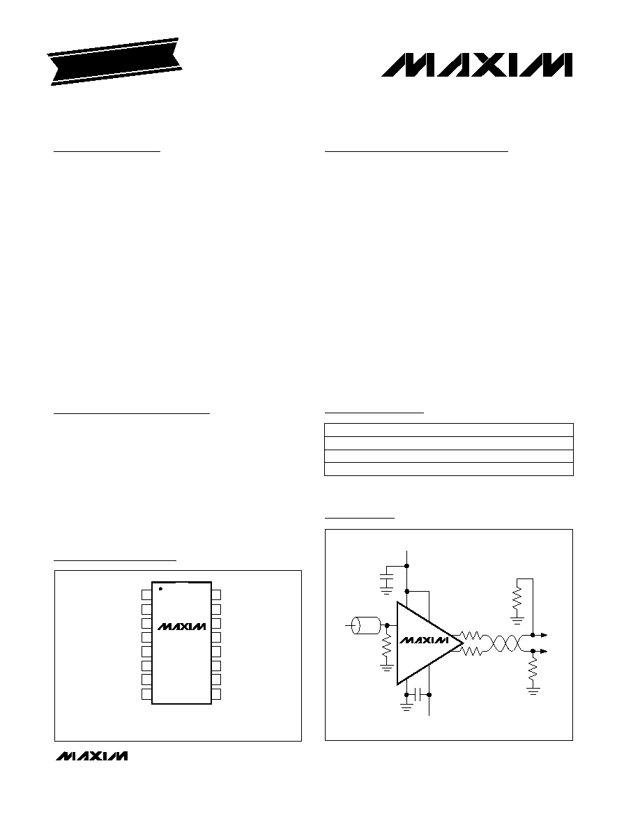
TOP VIEW
MAX4447
MAX4448
MAX4449
SO
V
CC
N.C.
N.C.
N.C. (RG)
IN
V
EE
V
EE
( ) ARE FOR MAX4448/MAX4449 ONLY
Typical Operating Circuit
19-1519 Rev 1; 10/99
PART
MAX4447ESE
MAX4448ESE
-40°C to +85°C
-40°C to +85°C
TEMP. RANGE
PIN-PACKAGE
16 Narrow SO
16 Narrow SO
Pin Configuration
Ordering Information
MAX4449ESE
-40°C to +85°C
16 Narrow SO
EVALUATION KIT
AVAILABLE
For price, delivery, and to place orders, please contact Maxim Distribution at 1-888-629-4642,
or visit Maxim's website at www.maxim-ic.com.

MAX4447/MAX4448/MAX4449
6500V/µs, Wideband, High-Output-Current, Single-
Ended-to-Differential Line Drivers with Enable
2
_______________________________________________________________________________________
ABSOLUTE MAXIMUM RATINGS
DC ELECTRICAL CHARACTERISTICS
(V
CC
= +5V, V
EE
= -5V, V
EN
2V, V
OUT
= V
OUT+
- V
OUT-
, R
L
=
, T
A
= T
MIN
to T
MAX,
unless otherwise noted. Typical values are at
T
A
= +25°C.)
Stresses beyond those listed under "Absolute Maximum Ratings" may cause permanent damage to the device. These are stress ratings only, and functional
operation of the device at these or any other conditions beyond those indicated in the operational sections of the specifications is not implied. Exposure to
absolute maximum rating conditions for extended periods may affect device reliability.
V
CC
to V
EE
..........................................................................+12V
Voltage on IN, EN, OUT+, OUT-, RG ....(V
EE
- 0.3V) to (V
CC
+ 0.3V)
Output Short-Circuit Duration to GND ...........................Indefinite
Continuous Power Dissipation (T
A
= +70°C)
16-Pin Narrow SO (derate 20mW/°C above +70°C) ..1600mW
Operating Temperature Range ...........................-40°C to +85°C
Storage Temperature Range ............................-65°C to +150°C
Lead Temperature (soldering, 10s) .................................+300°C
V
IN
= 0, V
EN
V
IL
V
EN
= 5V
Guaranteed by gain-error test
V
EN
= 0
V
EE
guaranteed by PSRR test
V
CC
guaranteed by PSRR test
V
EN
= 0, V
OUT+
= V
OUT-
= 3.15V or -3.15V
V
S
= ±4.5V to ±5.5V
Short circuit to GND
R
L
= 20
between OUT+ and OUT-
R
L
= 50
between OUT+ and OUT-
-3.0V
V
IN
3.0V
V
IN
= 0
V
IN
= 0
R
L
= 100
between OUT+ and OUT-
V
IN
= 0
CONDITIONS
3.2
5.5
I
Q
Quiescent Current
mA
46
55
µA
0.8
10
I
IH
EN Logic Input High Current
µA
-2.5
10
I
IL
EN Logic Input Low Current
V
2
V
IH
EN Logic High Threshold
V
0.8
V
IL
EN Logic Low Threshold
µA
4
30
I
OUT(OFF)
Output Leakage Current
dB
53
75
PSRR
Power-Supply Rejection Ratio
mA
140
I
SC
Output Short-Circuit Current
mA
90
130
I
OUT
Output Current Drive
V
±5.2
±6.2
V
OUT
Output Voltage Swing
±6.3
±7.4
V
-6/A
V
+6/A
V
V
IN
Input Voltage Range
V
-5.5
-4.5
V
EE
4.5
5.5
V
CC
Operating Supply Voltage
Range
2
k
50
R
IN
Input Resistance
mV
1.3
50
V
OS
Input Offset Voltage
µV/°C
25
TC
VOS
Input Offset Voltage
Temperature Coefficient
µA
7
45
I
B
Input Bias Current
UNITS
MIN
TYP
MAX
SYMBOL
PARAMETER
MAX4447
-6V
V
OUT
6V
A
V
MAX4448/MAX4449
(Note 1)
Gain
V/V
2
×
(1+300/R
G
)
V
IN
= 0, V
EN
V
IH
-6V
V
OUT
6V
%
0.1
2
Gain Error
V
OUT
= 0
%/°C
-0.002
Gain Drift
MAX4447
MAX4447
MAX4448/MAX4449
MAX4448/MAX4449
-0.3
5
0.01
Large-Signal -3dB Bandwidth
MAX4447/MAX4448/MAX4449
6500V/µs, Wideband, High-Output-Current, Single-
Ended-to-Differential Line Drivers with Enable
_______________________________________________________________________________________
3
AC ELECTRICAL CHARACTERISTICS
(V
CC
= +5V, V
EE
= -5V, R
L
= 100
between OUT+ and OUT-, A
VCL
= +2V/V for MAX4447/MAX4448, A
VCL
= +5V/V for MAX4449,
V
OUT
= V
OUT
+ - V
OUT
-, T
A
= +25°C, unless otherwise noted.)
V
OUT
= 100mVp-p
CONDITIONS
MHz
400
BW
SS
Small-Signal -3dB Bandwidth
330
430
UNITS
MIN
TYP
MAX
SYMBOL
PARAMETER
MAX4447
MAX4448
MAX4449
250
MAX4449
V
OUT
= 2Vp-p
MHz
405
V
OUT
= 4Vp-p
310
285
MAX4447
MAX4448
MAX4449
320
260
250
MAX4447
MAX4448
MAX4449
V
OUT
= 8V step
6500
V
OUT
= 100mVp-p
SR
Slew Rate (Note 2)
4300
5700
MAX4447
MAX4448
MAX4449
V
OUT
= 2V step
V/µs
1800
V
OUT
= 4V step
1900
1700
MAX4447
MAX4448
MAX4449
3700
3000
3000
MAX4447
MAX4448
MAX4449
MHz
140
0.1dB Gain Flatness
40
200
MAX4447
MAX4448
MAX4449
V
OUT
= 8V step
850
t
RISE
Rise Time (Note 2)
1030
670
MAX4447
MAX4448
MAX4449
V
OUT
= 2V step
ps
740
V
OUT
= 4V step
520
720
MAX4447
MAX4448
MAX4449
660
820
720
MAX4447
MAX4448
MAX4449
V
OUT
= 8Vp-p
BW
LS
Large-Signal -3dB Bandwidth
MAX4447/MAX4448/MAX4449
6500V/µs, Wideband, High-Output-Current, Single-
Ended-to-Differential Line Drivers with Enable
4
_______________________________________________________________________________________
Note 1: R
G
is the gain resistor. See Figure 1.
Note 2: Input step voltage has <100ps rise (fall) time. Measured at the output from 10% to 90% (90% to 10%) levels.
Note 3: Includes the current noise contribution through the on-die feedback resistor.
AC ELECTRICAL CHARACTERISTICS (continued)
(V
CC
= +5V, V
EE
= -5V, R
L
= 100
between OUT+ and OUT-, A
VCL
= +2V/V for MAX4447/MAX4448, A
VCL
= +5V/V for MAX4449,
V
OUT
= V
OUT
+ - V
OUT
-, T
A
= +25°C, unless otherwise noted.)
µs
nV/
Hz
pA/
Hz
V
OUT
= 4V step
780
V
OUT
= 8V step
810
900
MAX4447
MAX4448
MAX4449
V
OUT
= 2V step
660
CONDITIONS
t
FALL
Fall Time (Note 2)
770
800
MAX4447
MAX4448
MAX4449
-78
8
f
C
= 5MHz
ps
900
900
1100
UNITS
MIN
TYP
MAX
SYMBOL
PARAMETER
MAX4447
MAX4448
MAX4449
dBc
Settling Time
-46
-62
f
C
= 20MHz
f
C
= 100MHz
NTSC, R
L
= 150
NTSC, R
L
= 150
0.01
DG
Differential Gain Error
0.02
DP
-46
2nd Harmonic Distortion
Differential Phase Error
f
C
= 100MHz
-62
-78
-78
f
C
= 100kHz
f
C
= 5MHz
f
C
= 20MHz
V
IN
= 1V, V
OUT
settle to within 1%
V
IN
= 1V, V
OUT
settle to within 1%
V
IN
= 1V, V
OUT
settle to within 1%
0.08
t
ON
Power-Up Time
µs
0.4
ns
55
Enable Time
Disable Time
V
IN
= 1V, V
OUT
settle to within 1%
f = 10MHz, each output to ground
f = 1MHz
f = 1MHz (Note 3)
1.0
Z
OUT±
Output Impedance
%
1.8
i
N
24
e
N
Input Noise Voltage Density
Input Noise Current Density
µs
0.5
t
OFF
Power-Down Time
V
OUT
= 2Vp-p
-54
3rd Harmonic Distortion
f
C
= 100MHz
-71
-86
-86
f
C
= 100kHz
f
C
= 5MHz
f
C
= 20MHz
ns
-78
f
C
= 100kHz
V
OUT
= 2Vp-p
SFDR
Spurious-Free Dynamic Range
dBc
degrees
Settle to 0.1%, V
OUT
= 2V step
V
OUT
= 2Vp-p
dBc

MAX4447/MAX4448/MAX4449
6500V/µs, Wideband, High-Output-Current, Single-
Ended-to-Differential Line Drivers with Enable
_______________________________________________________________________________________
5
4
-6
100k
1M
10M
100M
1G
MAX4447
SMALL-SIGNAL GAIN vs. FREQUENCY
(V
OUT
= 100mVp-p)
-4
MAX4447 TOC01
FREQUENCY (Hz)
GAIN (dB)
-2
0
2
3
-5
-3
-1
1
4
-6
100k
1M
10M
100M
1G
MAX4448
SMALL-SIGNAL GAIN vs. FREQUENCY
(V
OUT
= 100mVp-p)
-4
MAX4447 TOC02
FREQUENCY (Hz)
GAIN (dB)
-2
0
2
3
-5
-3
-1
1
4
-6
100k
1M
10M
100M
1G
MAX4449
SMALL-SIGNAL GAIN vs. FREQUENCY
(V
OUT
= 100mVp-p)
-4
MAX4447 TOC03
FREQUENCY (Hz)
GAIN (dB)
-2
0
2
3
-5
-3
-1
1
0.5
-0.5
100k
1M
10M
100M
1G
MAX4447
GAIN FLATNESS vs. FREQUENCY
(V
OUT
= 100mVp-p)
-0.3
MAX4447 TOC04
FREQUENCY (Hz)
GAIN (dB)
-0.1
0.1
0.3
0.4
-0.4
-0.2
0
0.2
0.5
-0.5
100k
1M
10M
100M
1G
MAX4448
GAIN FLATNESS vs. FREQUENCY
(V
OUT
= 100mVp-p)
-0.3
MAX4447 TOC05
FREQUENCY (Hz)
GAIN (dB)
-0.1
0.1
0.3
0.4
-0.4
-0.2
0
0.2
0.5
-0.5
100k
1M
10M
100M
1G
MAX4449
GAIN FLATNESS vs. FREQUENCY
(V
OUT
= 100mVp-p)
-0.3
MAX4447 TOC06
FREQUENCY (Hz)
GAIN (dB)
-0.1
0.1
0.3
0.4
-0.4
-0.2
0
0.2
4
-6
100k
1M
10M
100M
1G
MAX4447
LARGE-SIGNAL GAIN vs. FREQUENCY
(V
OUT
= 2Vp-p)
-4
MAX4447 TOC07
FREQUENCY (Hz)
GAIN (dB)
-2
0
2
3
-5
-3
-1
1
4
-6
100k
1M
10M
100M
1G
MAX4448
LARGE-SIGNAL GAIN vs. FREQUENCY
(V
OUT
= 2Vp-p)
-4
MAX4447 TOC08
FREQUENCY (Hz)
GAIN (dB)
-2
0
2
3
-5
-3
-1
1
4
-6
100k
1M
10M
100M
1G
MAX4449
LARGE-SIGNAL GAIN vs. FREQUENCY
(V
OUT
= 2Vp-p)
-4
MAX4447 TOC09
FREQUENCY (Hz)
GAIN (dB)
-2
0
2
3
-5
-3
-1
1
Typical Operating Characteristics
(V
CC
= +5V, V
EE
= -5V, V
EN
= +5V, V
OUT
= V
OUT+
- V
OUT-
, R
L
= 100
between OUT+ and OUT-, A
V
= +2V/V for MAX4447/MAX4448,
A
V
= +5V/V for MAX4449, T
A
= +25°C, unless otherwise noted.)