Äîêóìåíòàöèÿ è îïèñàíèÿ www.docs.chipfind.ru
EVALUATION KIT
AVAILABLE
For free samples & the latest literature: http://www.maxim-ic.com, or phone 1-800-998-8800.
For small orders, phone 408-737-7600 ext. 3468.
General Description
The MAX4142 differential line driver combines high-
speed performance with fully symmetrical differential
inputs and outputs. With an internally set +2V/V closed-
loop gain, the MAX4142 is ideal for driving back-
terminated cables and transmission lines.
This device utilizes laser-trimmed thin-film resistors and
common-mode cancellation circuitry to deliver an out-
standing 67dB at 10MHz common-mode rejection
(CMR). Using current-feedback techniques, the
MAX4142 achieves a 250MHz -3dB (A
V
= +2V/V) band-
width, a 70MHz 0.1dB bandwidth, and a 1400V/µs slew
rate. Excellent differential gain/phase error and noise
specifications make this amplifier an excellent choice
for a wide variety of video and RF signal-processing
applications.
The MAX4142 operates from ±5V power supplies and
requires only 12.5mA of quiescent current. The output
stage is capable of driving a 100
load to ±6V (differ-
entially) or to ±3V (single-ended). The MAX4142 is
available in a space-saving 14-pin SO package. For a
pin-compatible, higher speed differential line driver,
see the MAX4147 data sheet.
________________________Applications
Video Twisted-Pair Driver
Differential Pulse Amplifier
High-Speed Instrumentation Amplifier
Low-Noise Differential Receivers
Differential ADC Driver
____________________________Features
o
250MHz -3dB Bandwidth (A
V
= +2V/V)
o
1400V/µs Slew Rate
o
67dB at 10MHz CMR
o
0.01%/0.01° Differential Gain/Phase
o
±6V Differentially into 100
Output Drive
o
1mA Shutdown Capability
o
12.5mA Quiescent Supply Current
o
Available in 14-Pin Narrow SO Package
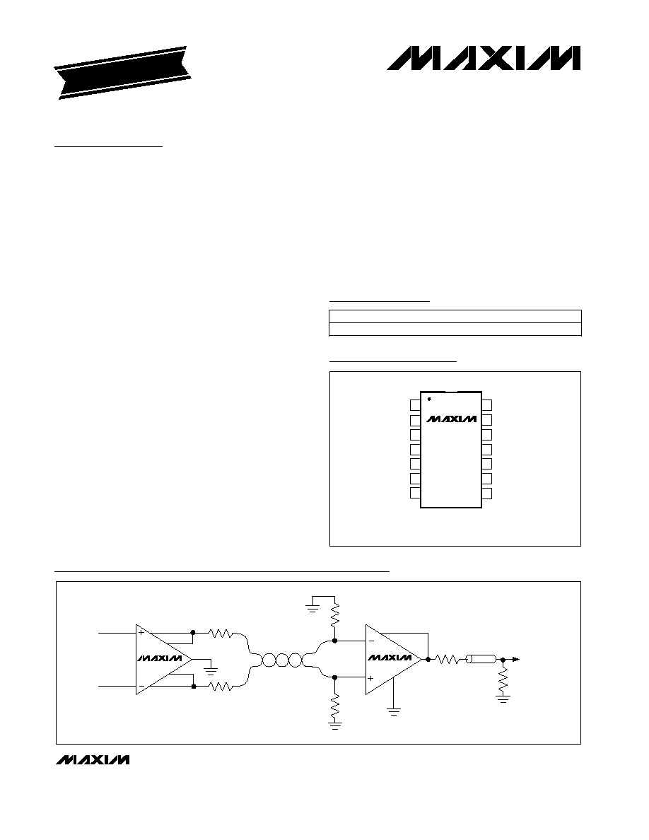
MAX4142
250MHz, Low-Power,
High-Output-Current, Differential Line Driver
________________________________________________________________
Maxim Integrated Products
1
GND
OUT+
IN+
IN-
IN-
SENSE
IN+
OUT-
SENSE-
SENSE+
R
t
R
t
R
t
R
t
OUT
REF
75
75
COAX
75
V
OUT
MAX4142
MAX4144
Typical Application Circuit
19-4763; Rev 0; 7/98
Ordering Information
TWISTED-PAIR TO COAX-CABLE CONVERTER
PART
MAX4142ESD
TEMP. RANGE
-40°C to +85°C
PIN-PACKAGE
14 SO
Pin Configuration
14
13
12
11
10
9
8
1
2
3
4
5
6
7
V
CC
OUT+
SENSE+
GND
SHDN
N.C.
IN+
V
EE
TOP VIEW
MAX4142
SENSE-
OUT-
V
CC
V
EE
IN-
N.C.
SO
N.C. = NOT INTERNALLY CONNECTED
MAX4142
250MHz, Low-Power, High-Output-Current,
Differential Line Driver
2
_______________________________________________________________________________________
ABSOLUTE MAXIMUM RATINGS
DC ELECTRICAL CHARACTERISTICS
(V
CC
= +5V, V
EE
= -5V, SHDN = 0, R
L
=
, T
A
= T
MIN
to T
MAX
, unless otherwise noted. Typical values specified at T
A
= +25°C.)
Stresses beyond those listed under "Absolute Maximum Ratings" may cause permanent damage to the device. These are stress ratings only, and functional
operation of the device at these or any other conditions beyond those indicated in the operational sections of the specifications is not implied. Exposure to
absolute maximum rating conditions for extended periods may affect device reliability.
Supply Voltage (V
CC
to V
EE
)................................................+12V
Voltage on Any Pin to Ground..........(V
EE
- 0.3V) to (V
CC
+ 0.3V)
Input Current (IN_)............................................................±10mA
Short-Circuit Duration (V
OUT
to GND) ................................10sec
Continuous Power Dissipation (T
A
= +70°C)
Plastic SO (derate 8.3mW/°C above +70°C) ................667mW
Operating Temperature Range ...........................-40°C to +85°C
Storage Temperature Range .............................-65°C to +150°C
Lead Temperature (soldering, 10sec) .............................+300°C
Differential Input Voltage Range
-3.0
3.0
V
Guaranteed by output voltage swing test
SHDN Input Current
I
SHDN
66
150
µA
V
SHDN
= 0
Output Resistance
R
OUT
0.1
SHDN Logic-High Threshold
V
IH
2.0
V
SHDN Logic-Low Threshold
V
IL
0.8
V
Enable Time from Shutdown
t
ON
500
ns
Disable Time to Shutdown
t
OFF
3.5
µs
PARAMETER
SYMBOL
MIN
TYP
MAX
UNITS
Input Offset Current
I
OS
0.2
2.5
µA
Input Bias Current
I
B
10
25
µA
Input Capacitance
C
IN
1
pF
Differential Input Resistance
R
IN
1
M
Input Offset Voltage
Operating Supply Voltage
±4.5
±5.5
V
V
OS
0.4
8
mV
Input Offset Voltage Drift
TC
VOS
3
µV/°C
Common-Mode Input Voltage Range
V
CM
-1.7
1.7
V
Gain
A
V
2
V/V
Gain Error
0.3
2
%
Gain Drift
20
ppm/°C
Common-Mode Rejection
CMR
55
80
dB
Power-Supply Rejection
PSR
65
95
dB
Quiescent Supply Current
I
CC,
I
EE
12.5
18
mA
Shutdown Supply Current
I
CC, SHDN
1.0
2.0
mA
3.0
3.4
6.0
6.8
2.0
2.4
Output Voltage Swing
V
OUT
4.0
4.8
V
Output Current Drive
I
OUT
120
75
mA
CONDITIONS
Guaranteed by CMR test
-1V
V
OUT
1V, R
L
= 53
V
IN
= 0
V
IN
= 0
-1V
V
OUT
1V, R
L
= 53
R
L
= 53
V
CM
= ±1.7V
V
S
= ±4.5V to ±5.5V
V
IN
= 0
Guaranteed by PSR test
V
SHDN
2V, V
IN
= 0
V
IN
= 0
Single-ended, R
L
=
Differential, R
L
=
V
IN
= 0
Single-ended, R
L
= 26.5
Differential, R
L
= 53
R
L
= 20
MAX4142
250MHz, Low-Power, High-Output-Current,
Differential Line Driver
_______________________________________________________________________________________
3
AC ELECTRICAL CHARACTERISTICS
(V
CC
= +5V, V
EE
= -5V, SHDN = 0V, R
L
= 150
differential, T
A
= T
MIN
to T
MAX
, unless otherwise noted. Typical values specified at
T
A
= +25°C.)
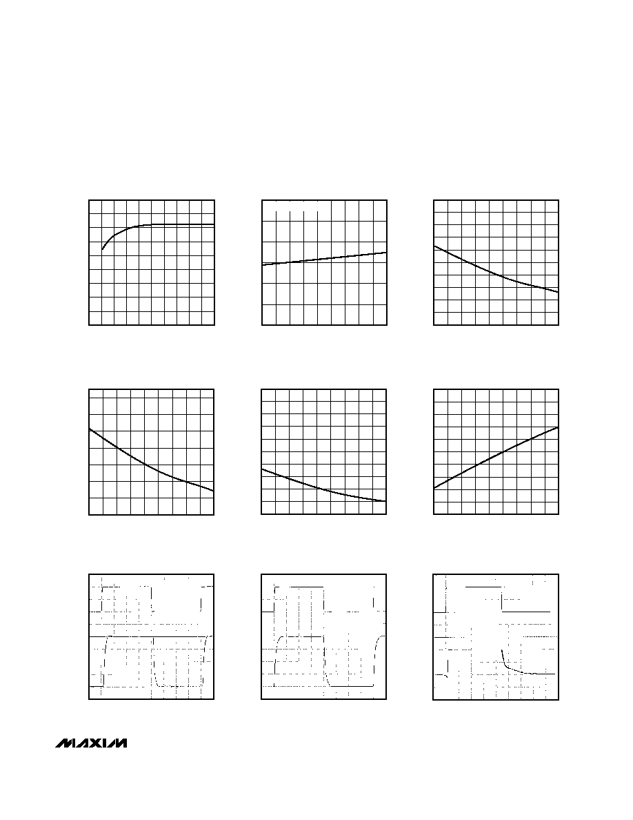
__________________________________________Typical Operating Characteristics
(V
CC
= +5V, V
EE
= -5V, SHDN = 0, R
L
= 150
differential, T
A
= +25°C, unless otherwise noted.)
10
0
0.1
10
1000
1
100
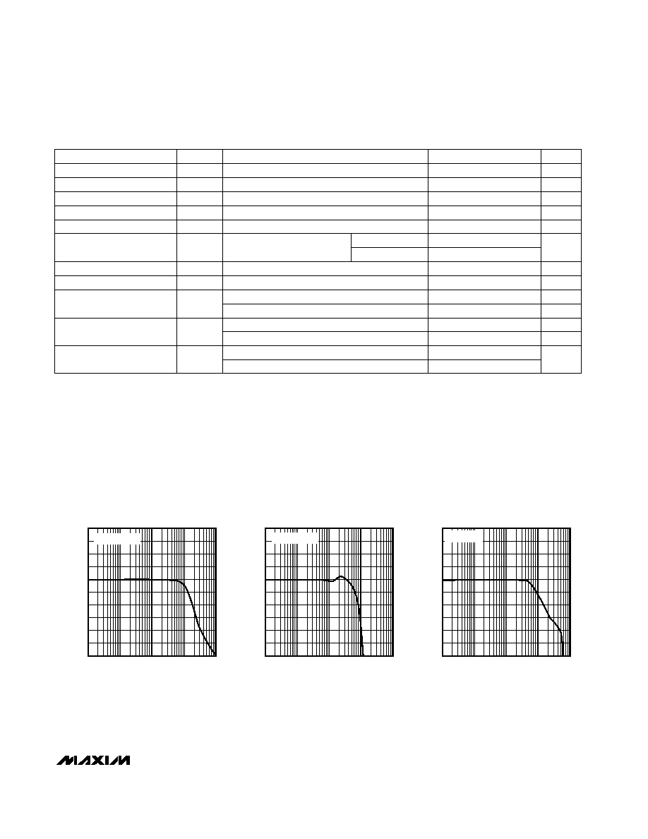
SMALL-SIGNAL GAIN
vs. FREQUENCY
2
MAX4142-01
FREQUENCY (MHz)
GAIN (dB)
4
6
8
9
1
3
5
7
V
OUT
= 100mVp-p
6.4
5.4
0.1
10
1000
1
100
GAIN FLATNESS vs. FREQUENCY
5.6
MAX4142-02
FREQUENCY (MHz)
GAIN (dB)
5.8
6.0
6.2
6.3
5.5
5.7
5.9
6.1
V
OUT
= 100mVp-p
10
0
0.1
10
1000
1
100
LARGE-SIGNAL GAIN
vs. FREQUENCY
2
MAX4142-03
FREQUENCY (MHz)
GAIN (dB)
4
6
8
9
1
3
5
7
V
OUT
= 2Vp-p
to 0.01%
to 0.1%
PARAMETER
SYMBOL
MIN
TYP
MAX
UNITS
Settling Time
t
S
45
25
ns
Slew Rate
SR
1400
V/µs
Common-Mode Rejection
CMR
67
dB
Differential Gain
DG
0.01
%
Differential Phase
DP
0.01
degrees
2
Input Current Noise
i
n
20
pA
Hz
Full-Power Bandwidth
-3dB Bandwidth
BW
(-3dB)
250
MHz
FPBW
180
MHz
0.1dB Bandwidth
BW
(0.1dB)
70
MHz
CONDITIONS
-1V
V
OUT
+1V
Differential, -2V
V
OUT
+2V
f = 10MHz, V
CM
= ±2V
f = 3.58MHz
f = 3.58MHz
f = 10kHz
f = 1MHz to 100MHz
V
OUT
0.1V
RMS
V
OUT
= 2Vp-p
V
OUT
0.1V
RMS
-84
Spurious-Free Dynamic
Range
SFDR
-76
dBc
f
C
= 500kHz, V
OUT
= 1Vp-p, R
S
= 50
, Figure1
f
C
= 10MHz, V
OUT
= 1Vp-p, R
S
= 50
, Figure1
8
Input Voltage Noise
e
n
80
nV/
Hz
f = 10kHz
f = 1MHz to 100MHz
µV
RMS
nA
RMS
MAX4142
250MHz, Low-Power, High-Output-Current,
Differential Line Driver
4
_______________________________________________________________________________________
_____________________________Typical Operating Characteristics (continued)
(V
CC
= +5V, V
EE
= -5V, SHDN = 0, R
L
= 150
differential, T
A
= +25°C, unless otherwise noted.)
10
110
0.1
10
1
100
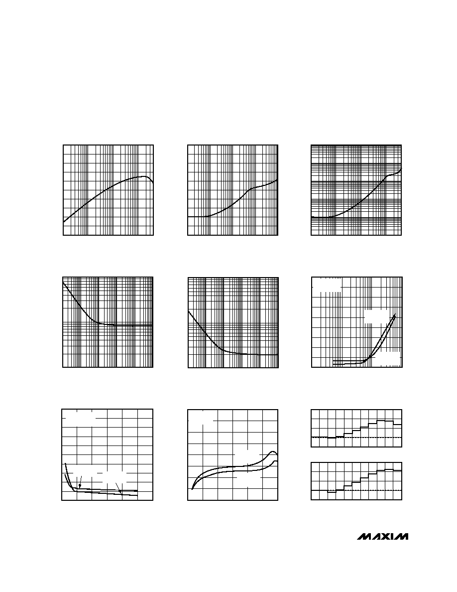
POWER-SUPPLY REJECTION
vs. FREQUENCY
90
MAX4142-04
FREQUENCY (MHz)
PSR (dB)
70
50
30
20
100
80
60
40
-10
90
0.1
10
1000
1
100
COMMON-MODE REJECTION
vs. FREQUENCY
70
MAX4142-05
FREQUENCY (MHz)
CMR (dB)
50
30
10
0
80
60
40
20
0.01
0.1
1
10
100
1000
0.1
10
1
100
OUTPUT IMPEDANCE vs. FREQUENCY
MAX4142-06
FREQUENCY (MHz)
OUTPUT IMPEDANCE (
)
1
10
100
10
100
1k
10k
100k
1M
VOLTAGE-NOISE DENSITY
vs. FREQUENCY
MAX4142-07
FREQUENCY (Hz)
VOLTAGE-NOISE DENSITY (nV/
Hz
)
-100
-90
-60
-80
-70
-50
-30
-40
-20
0
400
200
600
800
1000
1200
DISTORTION vs. LOAD
MAX4142-10
RESISTIVE LOAD (
)
DISTORTION (dBc)
2nd ORDER
HARMONIC
3rd ORDER
HARMONIC
f
O
= 5MHz,
V
OUT
= 1Vp-p
1
10
100
10
100
1k
10k
100k
1M
CURRENT-NOISE DENSITY
vs. FREQUENCY
MAX4142-08
FREQUENCY (Hz)
CURRENT-NOISE DENSITY (pA/
Hz
)
0.1
1
10
100
HARMONIC DISTORTION
vs. FREQUENCY
MAX4142-09
FREQUENCY (MHz)
DISTORTION (dBc)
-90
-70
-80
-40
-50
-60
-10
-20
-30
0
R
L
= 150
V
OUT
= 1Vp-p
2nd
HARMONIC
3rd
HARMONIC
-100
-90
-80
-70
-60
-50
-40
-30
-20
0
4
2
6
8
10
12
HARMONIC DISTORTION
vs. OUTPUT VOLTAGE SWING
MAX4142-11
OUTPUT VOLTAGE SWING (Vp-p)
DISTORTION (dBc)
f = 5MHz
R
L
= 150
2nd
HARMONIC
3rd
HARMONIC
-0.005
0
100
0
100
DIFFERENTIAL GAIN AND PHASE
-0.005
0.000
0.000
0.005
0.005
0.010
0.010
0.015
IRE
DIFF. PHASE (deg)
DIFF. GAIN (%)
MAX4142-12
MAX4142
250MHz, Low-Power, High-Output-Current,
Differential Line Driver
_______________________________________________________________________________________
5
0
4
2
8
6
10
12
16
14
18
0
100
200
300
400
500
DIFFERENTIAL OUTPUT SWING
vs. LOAD RESISTANCE
MAX4142-13
LOAD RESISTANCE (
)
OUTPUT SWING (Vp-p)
12
13
16
15
14
17
18
-45
-15
-30
0
15
30
45
60
75
90
DIFFERENTIAL OUTPUT VOLTAGE
SWING vs. TEMPERATURE
MAX4142-14
TEMPERATURE (°C)
DIFFERENTIAL OUTPUT VOLTAGE SWING (V)
R
L
= 1M
DIFFERENTIAL
0
0.2
0.1
0.4
0.3
0.6
0.5
0.7
0.9
0.8
1
-45
-15
0
15
-30
30
45
60
75
90
INPUT OFFSET VOLTAGE
vs. TEMPERATURE
MAX4142-15
TEMPERATURE (°C)
INPUT OFFSET VOLTAGE (mV))
5
9
7
15
13
11
19
17
-45
0
15
-30 -15
30
45
60
75
90
INPUT BIAS CURRENT
vs. TEMPERATURE
MAX4142-16
TEMPERATURE (°C)
INPUT BIAS CURRENT (
µ
A)
OUT
IN
GND
GND
TIME (10ns/div)
SMALL-SIGNAL PULSE RESPONSE
MAX4142-19
VOLTAGE (25mV/div)
0
0.2
0.1
0.4
0.3
0.6
0.5
0.7
0.9
0.8
1.0
-45
-15
0
15
-30
30
45
60
75
90
INPUT OFFSET CURRENT
vs. TEMPERATURE
MAX4142-17
TEMPERATURE (°C)
INPUT OFFSET CURRENT (
µ
A
)
10.0
11.0
10.5
12.0
11.5
13.0
12.5
13.5
14.5
14.0
15.0
-45
-15
0
15
-30
30
45
60
75
90
POWER-SUPPLY CURRENT
vs. TEMPERATURE
MAX4142-18
TEMPERATURE (°C)
POWER-SUPPLY CURRENT (mA)
OUT
IN
GND
GND
TIME (10ns/div)
LARGE-SIGNAL PULSE RESPONSE
MAX4142-20
VOLTAGE (500mV/div)
V
OUT
SHDN
0V
5V
0V
2V
TIME (2
µ
s/div)
ENABLE RESPONSE TIME
MAX4142-21
_____________________________Typical Operating Characteristics (continued)
(V
CC
= +5V, V
EE
= -5V, SHDN = 0, R
L
= 150
differential, T
A
= +25°C, unless otherwise noted.)