Äîêóìåíòàöèÿ è îïèñàíèÿ www.docs.chipfind.ru
General Description
The MAX4032 5V, 6dB video buffer with sync-tip clamp,
output sag correction, and low-power shutdown mode
is available in tiny SOT23 and SC70 packages. The
sag-corrected output of the MAX4032 is designed to
drive AC-coupled, 150
back-terminated video loads
in portable video applications such as digital still cams,
portable DVD players, digital camcorders, PDAs, video-
enabled cell phones, portable game systems, and
notebook computers. The sag correction feature intro-
duces low-frequency compensation that reduces the
value of the normally bulky and expensive 330µF AC-
coupling capacitor to two small, less expensive 22µF
capacitors. The input clamp positions the video wave-
form at the output and allows the MAX4032 to be used
as either an AC- or DC-coupled output driver.
The MAX4032 operates from a single +5V supply and
consumes only 6.5mA of supply current. The low-power
shutdown mode reduces the supply current to 150nA,
making the MAX4032 ideal for low-voltage, battery-
powered video applications.
The MAX4032 is available in tiny 6-pin SOT23 and
SC70 packages and is specified over the extended
-40
°C to +85°C temperature range.
Applications
Portable Video/Game Systems/DVD Players
Digital Camcorders/Televisions/Still Cameras
PDAs
Video-Enabled Cell Phones
Notebook Computers
Portable/Flat-Panel Displays
Features
o Single +5V Operation
o Input Sync-Tip Clamp
o AC- or DC-Coupled Output
o Low-Power Shutdown Mode Reduces Supply
Current to 150nA
o SAG Correction Reduces Output-Coupling
Capacitors from 330µF to 22µF
o Available in Space-Saving SOT23 and SC70
Packages
MAX4032
5V, 6dB Video Buffer with Sync-Tip Clamp,
Output Sag Correction, and 150nA Shutdown Current
________________________________________________________________ Maxim Integrated Products
1
PART
TEMP RANGE
PIN-
PACKAGE
TOP
MARK
MAX4032EXT-T
-40°C to +85°C
6 SC70-6
ACC
MAX4032EUT-T
-40°C to +85°C
6 SOT23-6
ABSP
Ordering Information
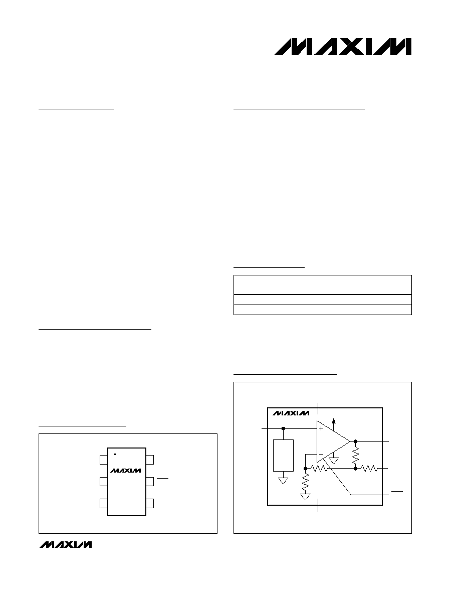
GND
V
CC
IN
1
6
SAG
5
SHDN
OUT
MAX4032
SC70/SOT23
TOP VIEW
2
3
4
Pin Configuration
19-3021; Rev 0; 10/03
For pricing, delivery, and ordering information, please contact Maxim/Dallas Direct! at
1-888-629-4642, or visit Maxim's website at www.maxim-ic.com.
MAX4032
CLAMP
1.2k
2.3k
580
780
IN
OUT
SAG
SHDN
GND
V
CC
TOP VIEW
Block Diagram
MAX4032
5V, 6dB Video Buffer with Sync-Tip Clamp,
Output Sag Correction, and 150nA Shutdown Current
2
_______________________________________________________________________________________
ABSOLUTE MAXIMUM RATINGS
DC ELECTRICAL CHARACTERISTICS
(V
CC
= 5.0V, GND = 0V, C
IN
= 0.1µF from IN to GND, R
L
= infinity to GND, SAG shorted to OUT, SHDN = 5.0V, T
A
= -40°C to +85°C.
Typical values are at T
A
= +25°C, unless otherwise noted.) (Note 2)
Stresses beyond those listed under "Absolute Maximum Ratings" may cause permanent damage to the device. These are stress ratings only, and functional
operation of the device at these or any other conditions beyond those indicated in the operational sections of the specifications is not implied. Exposure to
absolute maximum rating conditions for extended periods may affect device reliability.
Note 1: V
CLP
is the input clamp voltage as defined in the DC Electrical Characteristics table.
V
CC
to GND ............................................................. -0.3V to +6V
OUT, SAG, SHDN to GND......................... -0.3V to (V
CC
+ 0.3V)
IN to GND (Note 1) ................................... V
CLP
to (V
CC
+ 0.3V)
IN Short-Circuit Duration from -0.3V to V
CLP
........................1min
Output Short-Circuit Duration to V
CC
or GND .......... Continuous
Continuous Power Dissipation (T
A
= +70
°C)
6-Pin SOT23 (derate 8.7mW/°C above +70°C) ...........695mW
6-Pin SC70 (derate 3.1mW/°C above +70°C) .............245mW
Operating Temperature Range ..........................-40°C to +85°C
Junction Temperature .....................................................+150°C
Storage Temperature Range ............................-65°C to +150°C
Lead Temperature (soldering, 10s) ................................+300°C
PARAMETER
SYMBOL
CONDITIONS
MIN
TYP
MAX
UNITS
Supply Voltage Range
V
CC
Guaranteed by PSRR
4.5
5.5
V
Quiescent Supply Current
I
CC
V
IN
= V
CLP
6.5
10
mA
Shutdown Supply Current
I
SHDN
SHDN = 0V
0.15
1
µA
Input Clamp Voltage
V
CLP
Input referred
0.27
0.38
0.47
V
Input Voltage Range
V
IN
Inferred from voltage gain (Note 3)
V
CLP
1.45
V
Input Bias Current
I
BIAS
V
IN
= 1.45V
22.5
35
µA
Input Resistance
V
CLP
+ 0.5V < V
IN
< V
CLP
+ 1V
3
M
Voltage Gain
A
V
R
L
= 150
to GND, 0.5V < V
IN
< 1.45V
(Note 4)
1.9
2
2.1
V/V
Power-Supply Rejection Ratio
PSRR
4.5V < V
CC
< 5.5V
60
80
dB
Output Voltage High Swing
V
OH
R
L
= 150
to GND
4.3
4.6
V
Output Voltage Low Swing
V
OL
R
L
= 150
to GND
V
CLP
0.47
V
Sourcing, R
L
= 20
to GND
45
85
Output Current
I
OUT
Sinking, R
L
= 20
to V
CC
40
85
mA
Output Short-Circuit Current
I
SC
OUT shorted to V
CC
or GND
110
mA
SHDN Logic-Low Threshold
V
IL
V
CC
x 0.3
V
SHDN Logic-High Threshold
V
IH
V
CC
x 0.7
V
SHDN Input Current
I
IH
, I
IL
0.003
1
µA
At DC
4
Shutdown Output Impedance
R
OUT
(Disabled)
SHDN = 0V
At 3.58MHz or
4.43MHz
2
k
MAX4032
5V, 6dB Video Buffer with Sync-Tip Clamp,
Output Sag Correction, and 150nA Shutdown Current
_______________________________________________________________________________________
3
Note 2: All devices are 100% production tested at T
A
= +25°C. Specifications over temperature limits are guaranteed by design.
Note 3: Voltage gain (A
V
) is referenced to the clamp voltage, i.e., an input voltage of V
IN
= V
CLP
+ VI would produce an output volt-
age of V
OUT
= V
CLP
+ A
V
x VI.
Note 4: Droop is guaranteed by the input bias current specification.
AC ELECTRICAL CHARACTERISTICS
(V
CC
= 5.0V, GND = 0V, C
OUT
= C
SAG
= 22µF, C
IN
= 0.1µF, R
IN
= 75
to GND, R
L
= 150
to GND, SHDN = 5.0V, T
A
= +25°C,
unless otherwise noted.)
PARAMETER
SYMBOL
CONDITIONS
MIN
TYP
MAX
UNITS
Small-Signal -3dB Bandwidth
BW
SS
V
OUT
= 100mV
P-P
55
MHz
Large-Signal -3dB Bandwidth
BW
LS
V
OUT
= 2V
P-P
45
MHz
Small-Signal 0.1dB Gain Flatness
BW
0.1dBSS
V
OUT
= 100mV
P-P
18
MHz
Large-Signal 0.1dB Gain Flatness
BW
0.1dBLS
V
OUT
= 2V
P-P
17
MHz
Slew Rate
SR
V
OUT
= 2V step
275
V/µs
Settling Time to 0.1%
t
S
V
OUT
= 2V step
25
ns
Power-Supply Rejection Ratio
PSRR
f = 100kHz
50
dB
Output Impedance
Z
OUT
f = 5MHz
2.5
Differential Gain
DG
NTSC
0.4
%
Differential Phase
DP
NTSC
0.6
Degrees
Group Delay
D/dT
f = 3.58MHz or 4.43MHz
20
ns
Peak Signal to RMS Noise
SNR
V
IN
= 1V
P-P
, 10MHz BW
65
dB
Droop
C
IN
= 0.1µF (Note 4)
2
3
%
SHDN Enable Time
t
ON
V
IN
= V
CLP
+ 1V, SHDN = 5V, V
OUT
settled
to within 1% of the final voltage
250
ns
SHDN Disable Time
t
OFF
V
IN
= V
CLP
+ 1V, SHDN = 0V, V
OUT
settled
to below 1% of the output voltage
50
ns
MAX4032
5V, 6dB Video Buffer with Sync-Tip Clamp,
Output Sag Correction, and 150nA Shutdown Current
4
_______________________________________________________________________________________
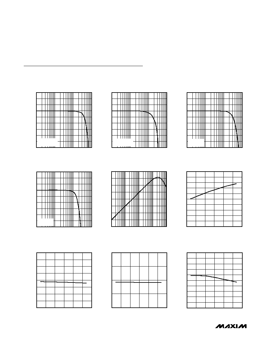
Typical Operating Characteristics
(V
CC
= 5.0V, GND = 0V, C
OUT
= C
SAG
= 22µF, C
IN
= 0.1µF, R
IN
= 75
to GND, R
L
= 150
to GND, SHDN = V
CC
, T
A
= +25°C,
unless otherwise noted.)
SMALL-SIGNAL GAIN
vs. FREQUENCY
MAX4032 toc01
FREQUENCY (Hz)
GAIN (dB)
10M
1M
-5
-4
-3
-2
-1
0
1
2
3
-6
100k
100M
A
V
= 2
V
OUT
= 100mV
P-P
SMALL-SIGNAL GAIN FLATNESS
vs. FREQUENCY
MAX4032 toc02
FREQUENCY (Hz)
GAIN (dB)
10M
1M
-0.5
-0.4
-0.3
-0.2
-0.1
0
0.1
0.2
0.3
-0.6
100k
100M
A
V
= 2
V
OUT
= 100mV
P-P
LARGE-SIGNAL GAIN
vs. FREQUENCY
MAX4032 toc03
FREQUENCY (Hz)
GAIN (dB)
10M
1M
-5
-4
-3
-2
-1
0
1
2
3
-6
100k
100M
A
V
= 2
V
OUT
= 2V
P-P
LARGE-SIGNAL GAIN FLATNESS
vs. FREQUENCY
MAX4032 toc04
FREQUENCY (Hz)
GAIN (dB)
10M
1M
-0.5
-0.4
-0.3
-0.2
-0.1
0
0.1
0.2
0.3
-0.6
100k
100M
A
V
= 2
V
OUT
= 2V
P-P
POWER-SUPPLY REJECTION RATIO
vs. FREQUENCY
MAX4032 toc05
FREQUENCY (Hz)
PSRR (dB)
10M
1M
100k
-70
-60
-50
-40
-30
-20
-10
0
-80
10k
100M
QUIESCENT SUPPLY CURRENT
vs. TEMPERATURE
MAX4032 toc06
TEMPERATURE (
°C)
SUPPLY CURRENT (mA)
75
50
25
0
-25
6.35
6.40
6.45
6.50
6.55
6.60
6.65
6.70
6.75
6.80
6.30
-50
100
CLAMP VOLTAGE
vs. TEMPERATURE
MAX4032 toc07
TEMPERATURE (
°C)
V
CLAMP
(V)
75
50
-25
0
25
0.25
0.30
0.35
0.40
0.45
0.50
0.55
0.60
0.20
-50
100
VOLTAGE GAIN vs. TEMPERATURE
MAX4032 toc08
TEMPERATURE (
°C)
GAIN (V/V)
75
50
25
0
-25
1.95
2.00
2.05
2.10
1.90
-50
100
OUTPUT VOLTAGE HIGH SWING
vs. TEMPERATURE
MAX4032 toc09
TEMPERATURE (
°C)
OUTPUT VOLTAGE HIGH (V)
75
50
25
0
-25
4.1
4.2
4.3
4.4
4.5
4.6
4.7
4.8
4.9
5.0
4.0
-50
100
5V, 6dB Video Buffer with Sync-Tip Clamp,
Output Sag Correction, and 150nA Shutdown Current
_______________________________________________________________________________________
5
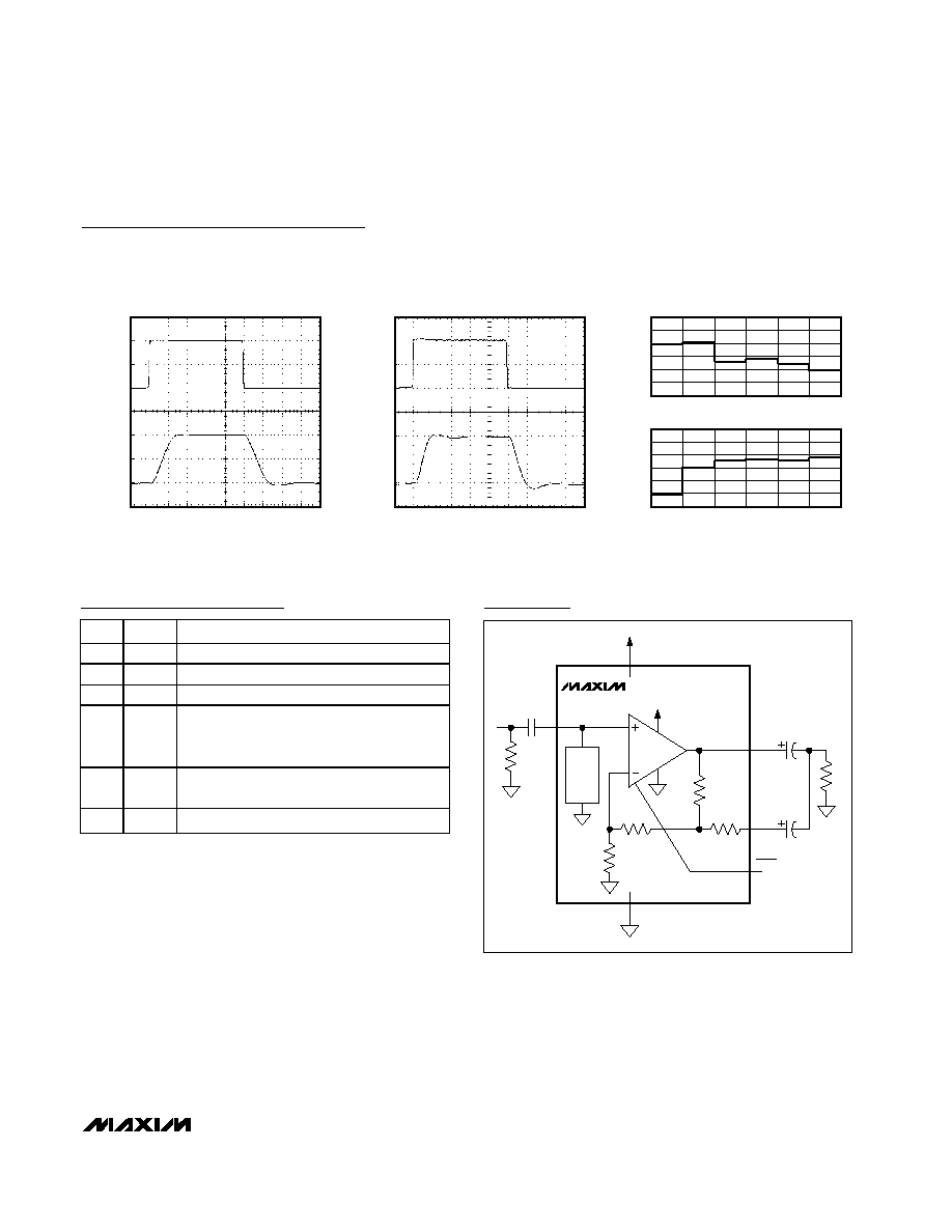
LARGE-SIGNAL PULSE RESPONSE
MAX4032 toc10
V
OUT
1V/div
V
IN
500mV/div
10ns/div
SMALL-SIGNAL PULSE RESPONSE
MAX4032 toc11
V
OUT
50mV/div
V
IN
25mV/div
10ns/div
DIFFERENTIAL GAIN AND PHASE
-0.8
0.4
DIFFERENTIAL
PHASE (
°
)
DIFFERENTIAL
GAIN (%)
MAX4032 toc12
0
1
2
3
4
5
6
0
1
2
3
4
5
6
-0.2
1.0
0.8
0.6
0.4
0.2
0
0.2
0
-0.2
-0.4
-0.6
MAX4032
Typical Operating Characteristics (continued)
(V
CC
= 5.0V, GND = 0V, C
OUT
= C
SAG
= 22µF, C
IN
= 0.1µF, R
IN
= 75
to GND, R
L
= 150
to GND, SHDN = V
CC
, T
A
= +25°C,
unless otherwise noted.)
Pin Description
PIN
NAME
FUNCTION
1
OUT
Video Output
2
GND
Ground
3
IN
Video Input
4
V
CC
Power-Supply Voltage. Bypass with a 0.1µF
capacitor to ground as close to the pin as
possible.
5
SHDN
Shutdown. Pull SHDN low to place the
MAX4032 in low-power shutdown mode.
6
SAG
Sag Correction
Typical Application Circuit
MAX4032
CLAMP
IN
OUT
SAG
GND
V
CC
SHDN
C
SAG
C
OUT
R
L
R
IN