General Description
The MAX3991 is a 10Gbps clock and data recovery
(CDR) with limiting amplifier IC for XFP optical receivers.
The MAX3991 and the MAX3992 (CDR with equalizer)
form a signal conditioner chipset for use in XFP trans-
ceiver modules. The chipset is XFI compliant and offers
multirate operation for data rates from 9.95Gbps to
11.1Gbps.
The MAX3991 has 7mV
P-P
input sensitivity (BER
10
-12
),
which allows direct connection to a transimpedance
amplifier without the use of a stand-alone limiting amplifi-
er. The phase-locked loop (PLL) is optimized for jitter tol-
erance and provides 0.6UI of high-frequency tolerance
in SONET, Ethernet, and Fibre-Channel applications. The
MAX3991 output provides 27% margin to the XFP eye
mask specification.
An AC-based power detector toggles the loss-of-signal
(LOS) output when the input signal swing is below the
user-programmed assert threshold. An external refer-
ence clock, with frequency equal to 1/64 or 1/16 of the
serial data rate is used to aid in frequency acquisition. A
loss-of-lock (LOL) indicator is provided to indicate the
lock status of the receiver PLL.
The MAX3991 is available in a 4mm x 4mm, 24-pin QFN
package. It consumes 350mW from a single +3.3V supply
and operates over the 0°C to +85°C temperature range.
Applications
9.95Gbps to 11.1Gbps Optical XFP Modules
SONET OC-192/SDH STM-64 XFP Transceivers
10.3Gbps/11.1Gbps Ethernet XFP Transceivers
10.5Gbps Fibre-Channel XFP Transceivers
10Gbps DWDM Transceivers
Features
Multirate Operation from 9.95Gbps to 11.1Gbps
7mV
P-P
Input Sensitivity (BER
10
-12
)
0.6UI
P-P
Total High-Frequency Jitter Tolerance
Low-Output Jitter Generation: 7mUI
RMS
Low-Output Deterministic Jitter: 4.6ps
P-P
XFI-Compliant Output Interface
LOS Indicator with Programmable Threshold
LOL Indicator
Power Dissipation: 350mW
MAX3991
10Gbps Clock and Data Recovery
with Limiting Amplifier
________________________________________________________________ Maxim Integrated Products
1
19-3486; Rev 0; 11/04
For pricing, delivery, and ordering information, please contact Maxim/Dallas Direct! at
1-888-629-4642, or visit Maxim's website at www.maxim-ic.com.
Ordering Information
PART
TEMP RANGE
PIN-
PACKAGE
PKG
CODE
MAX3991UTG
0°C to +85°C
24 QFN
T2444-4
MAX3991UTG+*
0°C to +85°C
24 QFN
T2444-4
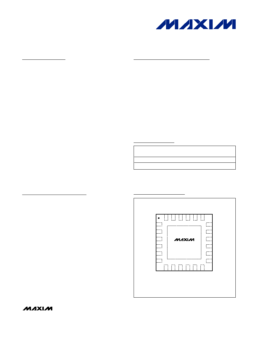
V
CC
1
GND
2
SDI+
3
SDI-
4
GND
5
V
CC
6
V
CC
18
GND
17
SDO+
16
SDO-
15
GND
14
V
CC
13
SCLKO+
7
SCLKO-
8
FCTL2
9
POL
10
V
CC
11
CFIL
12
VTH
24
FCTL1
23
REFCLK-
22
REFCLK+
21
LOS
20
LOL
19
MAX3991
4mm x 4mm QFN*
*THE EXPOSED PAD MUST BE CONNECTED TO CIRCUIT-BOARD GROUND FOR
PROPER THERMAL AND ELECTRICAL PERFORMANCE.
TOP VIEW
Pin Configuration
Typical Application Circuit appears at end of data sheet.
*Future product--contact factory for availability.
+Denotes lead-free package.

MAX3991
10Gbps Clock and Data Recovery
with Limiting Amplifier
2
_______________________________________________________________________________________
ABSOLUTE MAXIMUM RATINGS
Stresses beyond those listed under "Absolute Maximum Ratings" may cause permanent damage to the device. These are stress ratings only, and functional
operation of the device at these or any other conditions beyond those indicated in the operational sections of the specifications is not implied. Exposure to
absolute maximum rating conditions for extended periods may affect device reliability.
Supply Voltage, V
CC
..............................................-0.5V to +4.0V
Input Voltage Levels
(SDI+, SDI-, REFCLK+,
REFCLK-) ....................................(V
CC
- 1.0V) to (V
CC
+ 0.5V)
CML Output Voltage
(SDO+, SDO-, SCLKO+,
SLCKO-) ......................................(V
CC
- 1.0V) to (V
CC
+ 0.5V)
Voltage at (CFIL, LOL, VTH, POL,
LOS, FCTL1, FCTL2) ..............................-0.5V to (V
CC
+ 0.5V)
Continuous Power Dissipation (T
A
= +85
°C)
24-Pin QFN (derate 20.8mW/
°C above +85°C) .........1355mW
Junction Temperature Range ............................-40
°C to +150°C
Storage Temperature Range...........................-55
°C to +150°C
Lead Temperature (soldering, 10s) ............................+300
°C
ELECTRICAL CHARACTERISTICS
(See Table 1 for operating conditions. Typical values at V
CC
= +3.3V, T
A
= +25°C, unless otherwise noted.)
PARAMETER
SYM B O L
CONDITIONS
MIN
TYP
MAX
UNITS
Supply Current
I
CC
106
140
mA
DATA INPUT SPECIFICATION (SDI±)
Single-Ended Input Resistance
R
SE
42
50
58
Differential Input Resistance
R
D
84
100
116
Single-Ended Input Resistance
Matching
±5
%
0.1GHz to 5.5GHz (Note 1)
12.5
Differential Input Return Loss
SDD11
5.5GHz to 12GHz (Note 1)
6
dB
DC Cancellation Loop Low-
Frequency Cutoff
30
kHz
REFERENCE CLOCK SPECIFICATION (REFCLK±)
Single-Ended Input Resisitance
84
100
116
Differential Input Resistance
168
200
232
CML OUTPUT SPECIFICATION (SDO±)
SDO
± Differential Output Swing
(Note 2)
575
650
725
mV
P-P
SDO
± Output Common-Mode
Voltage
RL = 50
to V
CC
V
CC
-
0.16
V
SCLKO
± Differential Output
380
mV
P-P
Single-Ended Output Resistance
42
50
58
Differential Output Resistance
R
O
84
100
116
Single-Ended Output Resistance
Matching
±5
%
0.1GHz to 5.5GHz (Note 1)
13
Differential Output Return Loss
SDD22
5.5GHz to 12GHz (Note 1)
8
dB
Common-Mode Output Return
SCC22
0.1GHz to 15GHz (Note 1)
5
dB
Rise/Fall Time
(20% to 80%) (Note 2)
18
23
30
ps
Output AC Common Mode
(Note 2)
10
mV
RMS
Power-Down Assert Time
(Note 3)
50
µs

MAX3991
10Gbps Clock and Data Recovery
with Limiting Amplifier
_______________________________________________________________________________________
3
ELECTRICAL CHARACTERISTICS (continued)
(See Table 1 for operating conditions. Typical values at V
CC
= +3.3V, T
A
= +25°C, unless otherwise noted.)
PARAMETER
SYMBOL
CONDITIONS
MIN
TYP
MAX
UNITS
JITTER SPECIFICATION
120kHz < f
8MHz (Notes 2, 4)
0.05
0.25
Jitter Peaking
J
P
f
120kHz (Notes 2, 4)
0.03
dB
Jitter Transfer Bandwidth
J
BW
(Notes 2, 4)
5.6
8.0
MHz
f = 400kHz
3.0
>3
(Note 5)
f = 4MHz
0.55
>0.6 (Note 5)
Sinusoidal Jitter Tolerance
(Notes 2, 4, 6)
f = 80MHz
0.45
>0.5
(Note 5)
UI
P-P
Jitter Generation
(Notes 2, 4, 7)
4.5
11.0
m U I
RM S
Serial Data Output Deterministic
Jitter
DJ
PRBS 2
7
- 1 (Note 2)
4.6
13
ps
P-P
PLL ACQUISITION/LOCK SPECIFICATION
Acquisition Time
Figures 1, 2 (Note 2)
200
µs
LOL Assert Time
Figure 1 (Note 2)
90
µs
Maximum Frequency Pullin Time
(Note 8)
2
ms
Frequency Difference at which
LOL is Asserted
f/f
REFCLK
f = |f
VCO
/ N - f
REFCLK
|,
N = 16 or 64
651
ppm
Frequency Difference at which
LOL is DeAsserted
f/f
REFCLK
f = |f
VCO
/ N - f
REFCLK
|,
N = 16 or 64
500
ppm
LOSS-OF-SIGNAL (LOS) SPECIFICATION
VTH Control Voltage Range
VTH
150
500
mV
LOS Gain Factor
VTH/
V
LOS_ASSERT
10
V/V
Minimum LOS Assert Voltage
V
LOS_ASSERT
15
mV
Maximum LOS Assert Voltage
V
LOS_ASSERT
50
mV
LOS Gain-Factor Accuracy
(Notes 2, 9)
-1.5
+1.5
dB
LOS Hysteresis
(Notes 2, 10)
3.5
3.7
3.9
dB
LOS Gain-Factor Stability
(Note 2) Overtemperature and supply
-10
+10
%
LOS Assert Time
Figure 2 (Note 2)
3
90
µs
LOS Deassert Time
Figure 2 (Note 2)
90
µs
VTH Input Current
-5
+5
µA
LVTTL INPUT/OUTPUT SPECIFICATION (LOL, LOS, FCTL1, FCTL2)
Input High Voltage
V
IH
2.0
V
Input Low Voltage
V
IL
0.8
V
Input Current
-30
+30
µA
Output High Voltage
V
OH
Sourcing 30µA
V
CC
-
0.5
V
Output Low Voltage
V
OL
Sinking 1mA
0.4
V

MAX3991
10Gbps Clock and Data Recovery
with Limiting Amplifier
4
_______________________________________________________________________________________
ELECTRICAL CHARACTERISTICS (continued)
(See Table 1 for operating conditions. Typical values at V
CC
= +3.3V, T
A
= +25°C, unless otherwise noted.)
Note 1:
Measured with 100mV
P-P
differential amplitude.
Note 2:
Guaranteed by design and characterization.
Note 3:
Measured from the time that the FCTL1 input goes high with FCTL2 = 0 to the time when the supply current drops to less
than 40% of the nominal value.
Note 4:
Measured with PRBS = 2
31
- 1.
Note 5:
Measurement limited by test equipment.
Note 6:
Jitter tolerance is for BER
10
-12
, measured with additional 0.1UI deterministic jitter and 40mV
P-P
differential input.
Note 7:
Measured with 50kHz to 80MHz SONET filter.
Note 8:
Applies on power-up, after standby.
Note 9:
Over process, temperature, and supply.
Note 10: Hysteresis is defined as 20Log(V
LOS-DEASSERT
/ V
LOS-ASSERT
).
Table 2. Serial Data Rate and Reference Clock Frequency
APPLICATION
DATA RATE (Rb)
(Gbps)
/16 REFERENCE CLOCK
FREQUENCY (MHz)
/64 REFERENCE CLOCK
FREQUENCY (MHz)
OC-192 SONET SDH64
9.95328
622.08
155.52
OC-192 SONET Over FEC
10.664
666.5
166.625
ITU G.709
10.709
669.3125
167.328125
10Gbps Ethernet, IEEE 802.3ae
10.3125
644.53125
161.1328125
10 Gigabit Ethernet Over ITU G.709
11.09573
693.483125
173.3707813
10Gbps Fibre Channel
10.51875
657.421875
164.355469
Table 1. Operating Conditions (Unless otherwise noted, FCTL1 = FCTL2 = 0.)
PARAMETER
SYMBOL
CONDITIONS
MIN
TYP
MAX
UNITS
Supply Voltage
V
CC
3.0
3.6
V
Ambient Temperature
T
A
0
+85
°C
Input Data Rate
Rb
(See Tab l e 2 )
Gbps
S D I± D i ffer enti al Inp ut V ol tag e S w i ng
V
D
15
1000
mV
P-P
Load Resistance
RL
RL is AC-coupled
50
REFCLK± Differential Input Voltage
Swing
300
1600
mV
P-P
REFCLK Duty Cycle
30
70
%
Rb / 16
REFCLK Frequency
f
REFCLK
Rb / 64
GHz
REFCLK Accuracy
Relative to Rb / 16 or Rb / 64
-100
+100
ppm
f
REFCLK
= Rb / 64
1200
REFCLK Rise/Fall Times (20% to
80%)
f
REFCLK
= Rb / 16
300
ps
REFCLK Random Jitter
Noise bandwidth < 100MHz
10
ps
RMS
Note: The part should be in standby mode when data rates are being switched.

MAX3991
10Gbps Clock and Data Recovery
with Limiting Amplifier
_______________________________________________________________________________________
5
Figure 1. RX LOL Assert and PLL Acquisition Time
LOL
ACQUISITION
TIME
f/f
REFCLK
LOL
ASSERT TIME
*ASSERT AND ACQUISITION TIME ARE DEFINED
WITH A VALID REFERENCE CLOCK APPLIED.
651ppm
500ppm
Figure 2. LOS Assert/Deassert Time
LOS
LOS DEASSERT TIME
DATA INPUT
POWER
LOS ASSERT TIME
LOL
ACQUISITION TIME