_________________________________________________________________Maxim Integrated Products
1
For pricing, delivery, and ordering information, please contact Maxim/Dallas Direct! at
1-888-629-4642, or visit Maxim's website at www.maxim-ic.com.
MAX3657 Evaluation Kit
________________ General Description
The MAX3657 evaluation kit is a fully assembled chip-on-
board electrical demonstration kit that provides easy
evaluation of the MAX3657 155Mbps +3.3V trans-
impedance amplifier.
Note that the MAX3657 Evaluation Kit provides an
electrical interface to the IC that is similar, but not exactly
the same as a photodiode.
____________________________ Features
Easy +3.3V Electrical Evaluation of the MAX3657
Fully Assembled and Tested
EV Kit Designed for 50
Interfaces
______________ Ordering Information
PART TEMP. RANGE IC PACKAGE
MAX3657EVKIT -40°C to +85°C Dice
______________Component Suppliers
SUPPLIER
PHONE
FAX
AVX
843-444-2863
843-626-3123
Coilcraft
847-639-6400
847-639-1469
Digi-Key
218-681-6674
218-681-3380
EF Johnson
402-474-4800
402-474-4858
Murata
415-964-6321
415-964-8165
Note: Please indicate that you are using the MAX3657
when ordering from these suppliers.
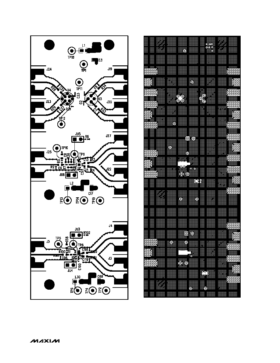
____________________ Component List
DESIGNATION QTY
DESCRIPTION
C2 C23
2
0.01
µF ± 5% Ceramic Capacitor
(0201) - Do not Install
C3
1
10
µF ±10% tantalum capacitor
Do Not Install
C4
1
0.9pF
± .075pF Ceramic
Capacitor (0402)
C5 C100
2
0.01
µF
± 10% Ceramic
Capacitor (0402)
C6, C7, C24,
C27
4
1
µF ± 5% Ceramic Capacitor
(0402) Do Not Install
C8, C9, C13,
C14, C96, C98,
C118, C119
8
1
µF ± 5% Ceramic Capacitor
(0402)
C17, C99
2
10
µF ±10% tantalum capacitor
C97
1
0.4pF
± 0.05pF Ceramic
Capacitor (0402)
J3 J4 J5, J22
J26 J27
6
SMA connectors
(edge-mount, round)
J19, J23, J24,
J25
4
SMA connectors
(edge-mount, round) Do not
Install
JU3, JU4, JU5,
JU6
4
2-pin headers (0.1in centers)
L1
1
56nH inductors (0805)
Coilcraft CS-560XKBC Do Not
Install
L2 L30
2
56nH inductors (0805)
Coilcraft CS-560XKBC
DESIGNATION QTY
DESCRIPTION
R2, R98
2
49.9
±1% resistor (0402)
R3, R4 R120,
R121
4
100
±1% resistor (0402)
R5 R100
2
10k
±1% resistor (0402)
R6
1
1k
±1% resistor (0402)
R7, R38
2
499
±1% resistor (0402)
R28-R29 R33-
R34
4
100
±1% resistor (0402) Do
Not Install
R31
1
1k
±1% resistor (0402) Do Not
Install
R99 R102 R103 3
4.99k
±1% resistor (0402)
TP2, TP4, TP5,
TP6 TP8, TP9,
TP10 TP13-
TP14, TP19
10
TESTPOINT DIGI-KEY 5000K-
ND
TP1, TP18,
TP11, TP12
4
TESTPOINT DIGI-KEY 5000K-
ND Do Not Install
U1
1
MAX3657 ETC 12 QFN
U2
1
MAX3657 DIE
U3
1
User Supplied 4 PIN TO CAN
U4
1
User Supplied 5 PIN TO CAN
19-2898; Rev 0, 5/03

MAX3657 Evaluation Kit
2
________________________________________________________________________________________
Evaluate: MAX3657
_________________________ Quick Start
Test Equipment Required
Test Equipment Required
Test Equipment Required
Test Equipment Required
·
+3.3V power supply with 100mA current capability
·
Signal-source, 155Mbps minimum capability
·
Oscilloscope with at least 100MHz performance
Procedure
Procedure
Procedure
Procedure
This procedure will set up the 12 Pin QFN section of the
evaluation board for 155Mbps operation.
1) Connect a signal source to J26 (IN). Set the signal
amplitude to 250mV
P-P
(Corresponding to 250
µA
P-P
current into the TIA). Set the data rate to 155Mbps.
2) Apply
150
µA to the DC_IN test point (TP10) using a
constant current source to emulate the DC
component of the input signal. A voltage source
connected from TP10 to GND may be used if a
constant current source is not available.
3) Connect OUT+ (J22) and OUT- (J27) to the 50
inputs of a high-speed oscilloscope.
4) Remove the shunt from JU6 to enable the DC
cancellation loop.
5) Install the shunt on JU5.to enable the average
current monitor.
6) Connect a 3.3V supply to the supply terminal (TP 13)
and to the GND terminal.
7) The differential signal at the oscilloscope should be
approximately 150mV
P-P
.
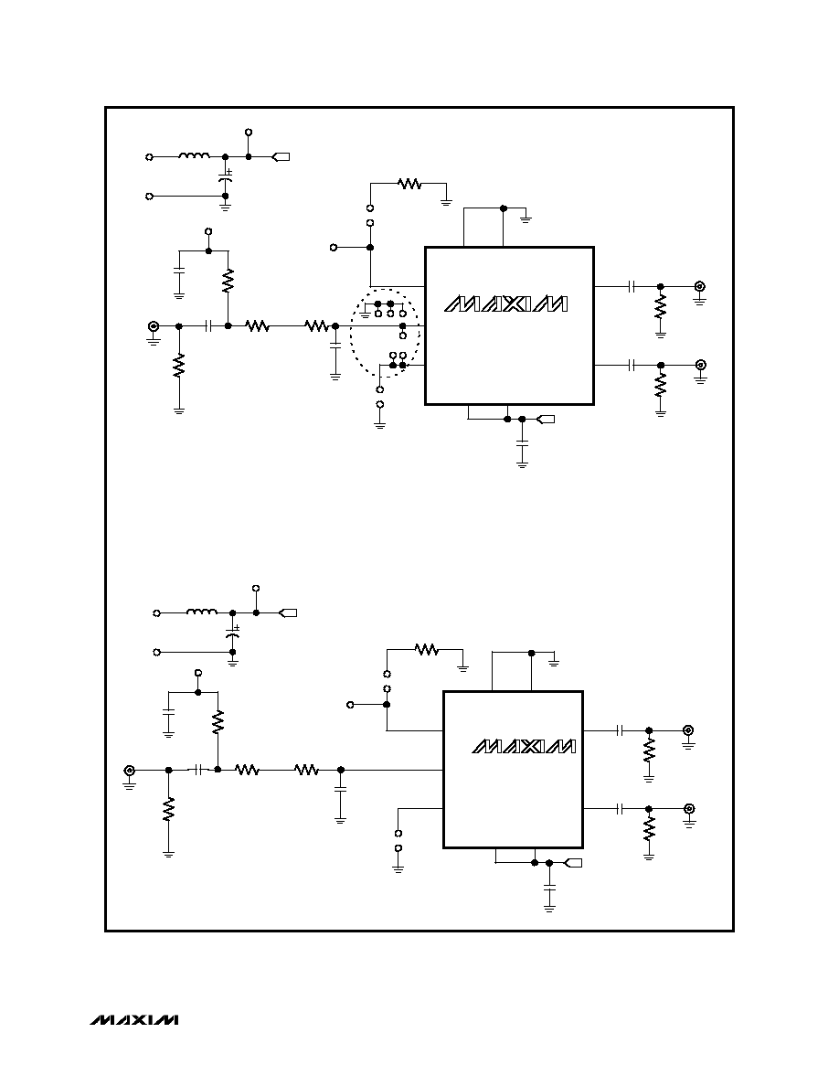
_______________ Detailed Description
The MAX3657 accepts a DC-coupled input from a high-
speed photodiode, for optical modulation amplitudes
ranging from -38dBm to 0dBm. The MAX3657 evaluation
board facilitates characterization of the MAX3657 TIA
with or without a photodiode. The MAX3657 comes from
the factory with the die attached and 12 pin QFN sections
completely assembled. The user must assemble the TO
header sections, if used.
Die Attached Section
Die Attached Section
Die Attached Section
Die Attached Section
The die-attached section provides a simple circuit for
emulating a photodiode current input. The connector at
IN (J1) is terminated with 50
to ground. Signal voltage
applied to the evaluation kit's input is AC coupled to a
resistance in series with the MAX3657's input, creating
an input signal current. Photodiode DC current can be
emulated by injecting DC current into the DC_IN_ pin.
12 Pin QFN Section
12 Pin QFN Section
12 Pin QFN Section
12 Pin QFN Section
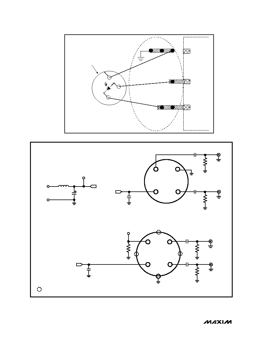
The 12 pin QFN section provides photodiode emulation
using similar circuitry as the die-bonded section. An
optional TO assembled photodiode interface is also
provided. To use a TO mounted photo diode, remove
R38, R7, and C4. Figure 2 shows a typical mounting
scheme for a photo diode in a TO header.
4 and 5 Pin TO Header Layout
4 and 5 Pin TO Header Layout
4 and 5 Pin TO Header Layout
4 and 5 Pin TO Header Layout
The TO header assembly layout provides a user-
assembled interface for evaluation of 4 and 5 pin TO
headers. (See the MAX3657 datasheet for a suggested
TO header layout.)
Test Equipment Interface
Test Equipment Interface
Test Equipment Interface
Test Equipment Interface
The MAX3657 outputs are back terminated with 100
ohms. To facilitate interface with 50
equipment, the
MAX3657 EV Kit places external 100
termination
resistors in parallel with each output so that the EV Kit
will match a 50
environment.
Note that the output load has a direct effect on the overall
gain and output signal swing. Because of the external
100
resistors, the overall gain is reduced by 50%. If
matching a 50
environment is not critical, higher gain
can be achieved by increasing the load resistance.
Photodiode Emulation
Photodiode Emulation
Photodiode Emulation
Photodiode Emulation
Use the following procedure to emulate the high-speed
current signal generated by a photodiode:
Select the desired optical power (PAVE in dBm) and
extinction ratio (re).
Calculate the average current (IAVE in Amps) as follows:
=
1000
10
I
)
10
/
P
(
AVG
AVE
where
is photodiode responsivity in A/W
Calculate the AC signal current (I
INPUT
in Amps
P-P
) as
follows, and adjust the signal generator to obtain it:
)
1
re
(
)
1
re
(
I
2
I
AVE
INPUT
+
-
=
For example, to emulate a signal with an average power
of -25dBm and an extinction ratio of 8.
-25dBm optical power will produce 2.7
µA of average
input current (assume a photodiode responsivity of
0.85A/W). Install a current meter between an external
DC source and the DC_IN test point. Adjust the source to
provide 2.7
µA.
The signal amplitude is 2I
AVE
(r
e
-1)/(r
e
+1) = 4.2
µA. To
generate this current through the two 4.99k
series input
resistors and the 800
internal resistance, set the signal
source to produce an output level of 45mV
P-P
.
Noise measurements
Noise measurements
Noise measurements
Noise measurements
Remove the input resistors and shunt capacitor before
attempting noise measurements. Be very careful when
working around the exposed bond wires of the die
bonded section. With the input resistors and shunt
capacitor removed, the total capacitance at the IN pin is
approximately 0.25pF for the die-attached section and
about 0.5pF for the QFN section.