
General Description
The MAX3657 is a transimpedance preamplifier for
receivers operating up to 155Mbps. The low noise, high
gain, and low-power dissipation make it ideal for Class-B
and Class-C passive optical networks (PONs).
The circuit features 14nA input-referred noise, 130MHz
bandwidth, and 2mA input overload. Low jitter is
achieved without external compensation capacitors.
Operating from a +3.3V supply, the MAX3657 con-
sumes only 76mW power. An integrated filter resistor
provides positive bias for the photodiode. These fea-
tures, combined with a small die size, allow easy
assembly into a TO-46 header with a photodiode. The
MAX3657 includes an average photocurrent monitor.
The MAX3657 has a typical optical sensitivity of -38dBm
(0.9A/W), which exceeds the Class-C PON require-
ments. Typical overload is 0dBm. The MAX3657 is avail-
able in die form with both output polarities (MAX3657E/D
and MAX3657BE/D.) The MAX3657 is also available in a
12-pin, 3mm x 3mm thin QFN package.
Applications
Optical Receivers (Up to 155Mbps Operation)
Passive Optical Networks (PONs)
SFP/SFF Transceivers
BiDi Transceivers
Features
14nA
RMS
Input-Referred Noise
54k Transimpedance Gain
130MHz (typ) Bandwidth
2mA
P-P
Input Current--0dBm Overload Capability
76mW (typ) Power Dissipation
3.3V Single-Supply Operation
Average Photocurrent Monitor
MAX3657
155Mbps Low-Noise Transimpedance
Amplifier
________________________________________________________________
Maxim Integrated Products
1
Ordering Information
19-2834; Rev 2; 2/04
For pricing, delivery, and ordering information, please contact Maxim/Dallas Direct! at
1-888-629-4642, or visit Maxim's website at www.maxim-ic.com.
*Dice are designed to operate over a -40�C to +110�C junction
temperature (T
J
) range, but are tested and guaranteed at T
A
=
+25�C.
Pin Configuration appears at end of data sheet.
PART
TEMP RANGE
PIN-PACKAGE
MAX3657ETC
-40�C to +85�C
12 Thin QFN
MAX3657E/D
-40�C to +85�C
Die*
MAX3657BE/D
-40�C to +85�C
Die*
Typical Application Circuit
FILT
IN
GND
1�F
1�F
TO-46 HEADER
*OPTIONAL COMPONENT
OUT+
OUT-
MON
V
CCZ
R
FILT
C
FILT
3.3V
C
OUT
R
LOAD
200
R
MON
*
LIMITING AMPLIFIER
MAX3964
MAX3657
V
CC
C
VCC1
C
VCC2
MAX3657
155Mbps Low-Noise Transimpedance
Amplifier
2
_______________________________________________________________________________________
ABSOLUTE MAXIMUM RATINGS
DC ELECTRICAL CHARACTERISTICS
(V
CC1
= +2.97V to +3.63V, 200 load between OUT+ and OUT-, T
A
= -40�C to +85�C. Typical values are at V
CC
= +3.3V, T
A
= +25�C,
unless otherwise noted.) (Note 1)
Stresses beyond those listed under "Absolute Maximum Ratings" may cause permanent damage to the device. These are stress ratings only, and functional
operation of the device at these or any other conditions beyond those indicated in the operational sections of the specifications is not implied. Exposure to
absolute maximum rating conditions for extended periods may affect device reliability.
Power-Supply Voltage ...........................................-0.5V to +6.0V
Input Continuous Current ................................................�3.5mA
Voltage at OUT+, OUT- ...................(V
CC
- 1.5V) to (V
CC
+ 0.5V)
Voltage at FILT, MON .................................-0.5V to (V
CC
+ 0.5V)
Continuous Power Dissipation
12-Pin QFN (derate 14.7mW/�C above +70�C) .........1176mW
Operating Temperature Range
12-Pin QFN ......................................................-40�C to +85�C
Operating Junction Temperature Range
Die .................................................................-40�C to +150�C
Storage Temperature Range .............................-55�C to +150�C
Lead Temperature (soldering, 10s) .................................+300�C
Die Attach Temperature...................................................+400�C
PARAMETER
SYMBOL
CONDITIONS
MIN
TYP
MAX
UNITS
Supply Current
I
CC
23
34
mA
Input Bias Voltage
V
IN
I
IN
1mA
1
1.3
V
Transimpedance Linear Range
0.95 < linearity < 1.05, referred to gain at
1�A
P-P
input
2
�A
P-P
Small-Signal Transimpedance
Z
21
Differential output, I
IN
< 200nA
P-P
44
54
65
k
Output Common-Mode Voltage
AC-coupled outputs
V
CC
-
0.225
V
Output Resistance (Per Side)
R
OUT
Single-ended output resistance
82
100
118
Maximum Differential Output Voltage
V
OUT(max)
I
IN
= 2mA
P-P,
V
OUT
= (V
OUT
+) - (V
OUT
-)
170
250
450
mV
P-P
Filter Resistor
R
FILT
640
800
960
DC Input Overload
1
1.5
mA
Monitor Nominal Gain
G
NOM
V
CC
= +3.3V, +25�C (Note 2)
0.8
1
1.2
A/A
I
IN
= 100�A to 1mA
-1.5
+1.5
Die
-1.5
+2.2
I
IN
= 5�A
QFN package
-3.0
+2.7
I
IN
= 2�A
Die only
-4.0
+3.4
Monitor Gain Stability
(Note 3)
G
I
IN
= 1�A
Die only
�2.0
dB
AC ELECTRICAL CHARACTERISTICS
(V
CC
= +2.97V to +3.63V, 200 load between OUT+ and OUT-, C
IN
= 0.5pF, C
FILT
= 400pF, C
VCC2
= 680pF, T
A
= -40�C to +85�C.
Typical values are at V
CC
= +3.3V, T
A
= +25�C, unless otherwise noted.) (Note 1)
PARAMETER
SYMBOL
CONDITIONS
MIN
TYP
MAX
UNITS
Small-Signal Bandwidth
BW
-3dB
Relative to gain at 1MHz
110
MHz
Low-Frequency Cutoff
-3dB, I
IN
= 1�A
5
25
kHz
AC Overload
2
mA
P-P
Pulse-Width Distortion
PWD
300nA
P-P
I
IN
2mA
P-P
22
ps
P-P
f = 100MHz (Note 4)
15
Input-Referred Noise Current
I
n
f = 117MHz
14
nA
RMS
RMS Noise Density
f = 100MHz
1.3
pA/Hz
Monitor Bandwidth
I
IN
= 1�A
5
kHz
MAX3657
155Mbps Low-Noise Transimpedance
Amplifier
_______________________________________________________________________________________
3
Note 1: Die parameters are production tested at room temperature only, but are guaranteed by design from T
A
= -40�C to +85�C.
AC characteristics guaranteed by design and characterization.
Note 2: G
NOM
= I
MON
(1mA) / 1mA.
Note 3: Stability is relative to the nominal gain at V
CC
= +3.3V, T
A
= +25�C. G(I
IN
) dB = 10 log
10
[ I
MON
(I
IN
) ] / [ I
MON
(1mA) - G
NOM
x (1mA - I
IN
)], V
MON
2.1V, Input t
r,
t
f
> 550ps (20% to 80%).
Note 4: Total noise integrated from 0 to f.
AC ELECTRICAL CHARACTERISTICS (12-PIN QFN)
(V
CC
= +2.97V to +3.63V, R
LOAD
= 200, C
IN
= 1.0pF, C
FILT
= 1000pF, C
VCC2
= 0.01�F, T
A
= -40�C to +85�C. Typical values are at
V
CC
= +3.3V, T
A
= +25�C, unless otherwise noted.) (Note 1)
PARAMETER
SYMBOL
CONDITIONS
MIN
TYP
MAX
UNITS
Small-Signal Bandwidth
BW
-3dB
Relative to gain at 1MHz
95
MHz
Low-Frequency Cutoff
-3dB, I
IN
= 1�A
5
25
kHz
AC Overload
r
10
1.6
mA
Pulse-Width Distortion
PWD
1�A
P-P
I
IN
2mA
P-P
22
ps
P-P
f = 50MHz (Note 4)
5
Input-Referred Noise Current
I
n
f = 100MHz
13
nA
RMS
RMS Noise Density
f = 100MHz
1.3
pA/
Hz
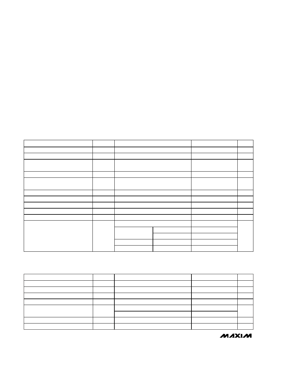
Typical Operating Characteristics
(MAX3657 E/D. V
CC
= 3.3V, C
IN
= 0.5pF, T
A
= +25�C, unless otherwise noted.)
35
40
50
45
55
60
-40
0
20
-20
40
60
80
SMALL-SIGNAL TRANSIMPEDANCE
vs. TEMPERATURE
MAX3657 toc01
AMBIENT TEMPERATURE (�C)
TRANSIMPEDANCE GAIN (k
)
0.2�A
P-P
1.0�A
P-P
0
30
20
10
70
60
80
50
40
90
100
-40
0
20
-20
40
60
80
SUPPLY CURRENT
vs. TEMPERATURE
MAX3657 toc02
AMBIENT TEMPERATURE (�C)
SUPPLY CURRENT (mA)
0.7
0.9
0.8
1.1
1.0
1.2
1.3
-40
0
20
-20
40
60
80
INPUT BIAS VOLTAGE
vs. TEMPERATURE
MAX3657 toc03
AMBIENT TEMPERATURE (�C)
INPUT BIAS VOLTAGE (V)
OUTPUT EYE DIAGRAM
(1.0�A ELECTRICAL INPUT)
MAX3657 toc10
1ns/div
50mV
-50mV
10mV
OUTPUT EYE DIAGRAM
(100�A ELECTRICAL INPUT)
MAX3657 toc11
1ns/div
200mV
-200mV
40mV
OUTPUT EYE DIAGRAM
(1mA ELECTRICAL INPUT)
MAX3657 toc12
1ns/div
200mV
-200mV
40mV
MAX3657
155Mbps Low-Noise Transimpedance
Amplifier
4
_______________________________________________________________________________________
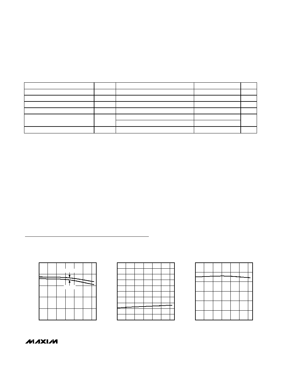
Typical Operating Characteristics (continued)
(MAX3657 E/D. V
CC
= 3.3V, C
IN
= 0.5pF, T
A
= +25�C, unless otherwise noted.)
100
0
0.1
1
10
100
1000
10,000
PULSE-WIDTH DISTORTION
vs. INPUT CURRENT AMPLITUDE
20
MAX3657 toc04
INPUT SIGNAL AMPLITUDE (�A)
PULSE-WIDTH DISTORTION (ps)
40
60
80
10
30
50
70
90
+85�C
+25�C
-40�C
-400
-200
-300
0
-100
100
200
300
400
-20
-10
-5
-15
0
5
10
15
20
DIFFERENTIAL OUTPUT VOLTAGE
vs. INPUT CURRENT
MAX3657 toc05
INPUT CURRENT (�A)
OUTPUT VOLTAGE (mV
P-P
)
V
FILT
= GND
R
LOAD
= OPEN
Z
21
= 108k
R
LOAD
= 200
Z
21
= 54k
R
LOAD
= 100
Z
21
= 36k
FREQUENCY RESPONSE
FREQUENCY (Hz)
OUTPUT MAGNITUDE
(dB
)
98
80
83
86
89
95
92
100
1M
100M
10k
1k
100k
10M
1G
MAX3657 toc06
DIFFERENTIAL OUTPUT
SINGLE-ENDED OUTPUT
0
50
25
175
150
225
250
200
100
75
125
275
0.1
0.5
0.7
0.3
0.9
1.1
1.3
1.5
BANDWIDTH vs. CAPACITANCE
MAX3657 toc07
CAPACITANCE (pF)
BANDWIDTH (MHz)
T
J
= +110�C
T
J
= +25�C
T
J
= -40�C
0
10
20
15
25
30
35
0.2
0.4
0.6
0.8
1.0
1.2
1.4
INPUT-REFERRED RMS NOISE
vs. CAPACITANCE
MAX3657 toc08
CAPACITANCE (pF)
INPUT-REFERRED NOISE (nA
RMS
)
T
J
= -40�C
T
J
= +25�C
T
J
= +110�C
1.2
0
0.1
1
10
100
1000
10,000
INPUT-REFERRED RMS NOISE
vs. DC INPUT CURRENT
0.2
MAX3657 toc09
DC CURRENT IN (�A)
INPUT-REFERRED NOISE (nA
RMS
) 1.0
0.4
0.6
0.8
T
J
= +110�C
T
J
= +25�C
T
J
= -40�C

MAX3657
155Mbps Low-Noise Transimpedance
Amplifier
_______________________________________________________________________________________
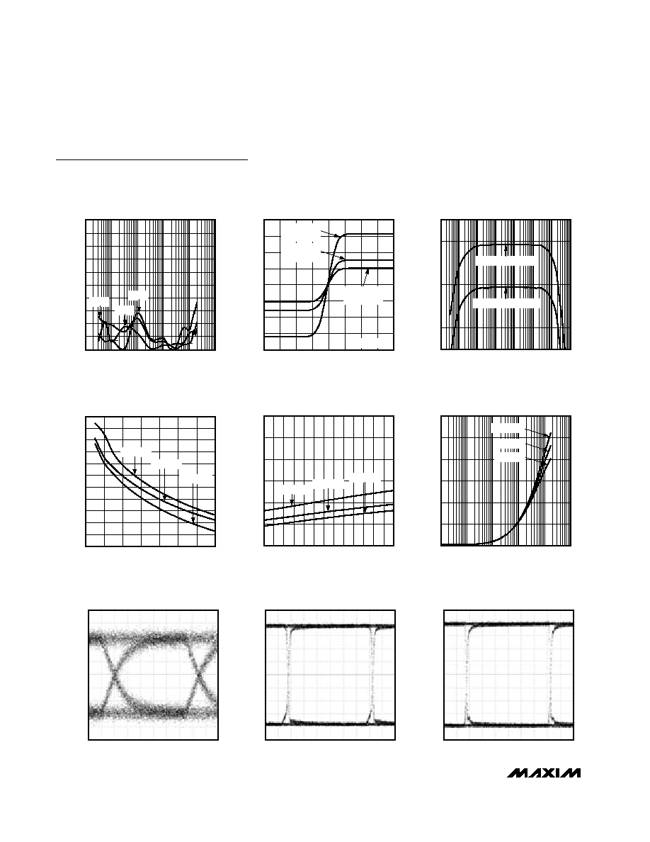
5
OUTPUT EYE DIAGRAM
(-30dBm OPTICAL INPUT)
MAX3657toc13
1ns/div
6mV/
div
ZARLINK 1A358 PHOTODIODE + MAX3657
2
23-1
PRBS
OUTPUT EYE DIAGRAM
(-1dBm OPTICAL INPUT)
MAX3657toc14
1ns/div
20mV/
div
ZARLINK 1A358 PHOTODIODE + MAX3657
2
23-1
PRBS
INPUT IMPEDANCE vs. FREQUENCY
FREQUENCY (Hz)
MAGNITUDE OF INPUT IMPEDANCE
(
)
800
300
350
400
450
500
550
600
750
700
650
100
1M
100M
10k
1k
100k
10M
1G
MAX3657 toc15
T
J
= +25�C
T
J
= -40�C
T
J
= +110�C
SMALL SIGNAL
Typical Operating Characteristics (continued)
(MAX3657 E/D. V
CC
= 3.3V, C
IN
= 0.5pF, T
A
= +25�C, unless otherwise noted.)
PIN
NAME
FUNCTION
1, 9, 11
N.C.
No Connection. Do not connect.
2
GND
Negative Supply Voltage. Both GND and GNDZ must be connected to ground.
3
GNDZ
Negative Supply Voltage. Both GND and GNDZ must be connected to ground.
4
MON
Photocurrent Monitor. This is a current output. Connect a resistor between MON and ground to monitor the
average photocurrent.
5
IN
Signal Input. Connect to photodiode anode.
6
FILT
Filter Connection (Optional). Use to bias the photodiode cathode. An internal 800
on-chip resistor is connected
between this pin and V
CCZ
; an external decoupling capacitor connected to this pin forms a filter (see the Design
Procedure section).
7
V
CCZ
Power-Supply Voltage. Both V
CC
and V
CCZ
must be connected to the supply.
8
V
CC
Power-Supply Voltage. Both V
CC
and V
CCZ
must be connected to the supply.
10
OUT+
Positive Data Output. This output has 100
back termination, increasing input current causes OUT+ to increase.
12
OUT-
Negative Data Output. This output has 100
back termination, increasing input current causes OUT- to decrease.
Pin Description