
_______________General Description
The MAX364/MAX365 are precision, quad, single-pole
single-throw (SPST) analog switches. The MAX364 has
four normally closed (NC), and the MAX365 has four
normally open (NO) switches. Both parts offer low-
channel on resistance (less than 85
), guaranteed to
match within 2
between channels and to remain flat
over the analog signal range (
9
max). Both parts
also offer low leakage (less than 500pA at +25°C and
less than 4nA at +85°C) and fast switching (turn-on
time less than 250ns and turn-off time less than 170ns).
The MAX364/MAX365 are fabricated with Maxim's new
improved 44V silicon-gate process. Design improve-
ments guarantee extremely low charge injection
(10pC), low power consumption (35µW), and electro-
static discharge (ESD) greater than 2000V. The 44V
maximum breakdown voltage allows rail-to-rail analog
signal handling capability.
These monolithic switches operate with a single positive
supply (+10V to +30V) or with split supplies (±4.5V to
±20V) while retaining CMOS-logic input compatibility
and fast switching. CMOS inputs provide reduced
input loading.
________________________Applications
Sample-and-Hold Circuits
Communication Systems
Guidance and Control Systems Battery-Operated Systems
Heads-Up Displays
PBX, PABX
Test Equipment
Military Radios
____________________________Features
o
Low On Resistance: < 45
Typical (85
Max)
o
Guaranteed Matched On Resistance Between
Channels: < 2
o
Guaranteed Flat On Resistance over Full Analog
Signal Range:
9
Max
o
Guaranteed Charge Injection: < 10pC
o
Guaranteed Off-Channel Leakage: < 4nA at +85°C
o
ESD Guaranteed > 2000V per Method 3015.7
o
Single-Supply Operation (+10V to +30V)
Bipolar-Supply Operation (±4.5V to ±20V)
o
TTL-/CMOS-Logic Compatible
o
Rail-to-Rail Analog Signal Handling Capability
______________Ordering Information
* Contact factory for dice specifications.
MAX364/MAX365
Precision, Quad, SPST Analog Switches
________________________________________________________________
Maxim Integrated Products
1
Call toll free 1-800-998-8800 for free samples or literature.
PART
TEMP. RANGE
PIN-PACKAGE
MAX364
CPE
0°C to +70°C
16 Plastic DIP
MAX364CSE
0°C to +70°C
16 Narrow SO
MAX364C/D
0°C to +70°C
Dice*
MAX364EPE
-40°C to +85°C
16 Plastic DIP
MAX364ESE
-40°C to +85°C
16 Narrow SO
MAX365
CPE
0°C to +70°C
16 Plastic DIP
16
15
14
13
12
11
10
9
1
2
3
4
5
6
7
8
IN2
COM2
NO2
V+
V-
NO1
COM1
IN1
MAX365
VL
NO3
COM3
IN3
IN4
COM4
NO4
GND
DIP/SO
DIP/SO
MAX365
LOGIC
SWITCH
0
1
OFF
ON
SWITCHES SHOWN FOR LOGIC "0" INPUT
MAX364
LOGIC
SWITCH
0
1
ON
OFF
16
15
14
13
12
11
10
9
1
2
3
4
5
6
7
8
IN2
COM2
NC2
V+
V-
NC1
COM1
IN1
MAX364
VL
NC3
COM3
IN3
IN4
COM4
NC4
GND
TOP VIEW
_____________________Pin Configurations/Functional Diagrams/Truth Tables
MAX365CSE
0°C to +70°C
16 Narrow SO
MAX365C/D
0°C to +70°C
Dice*
MAX365EPE
-40°C to +85°C
16 Plastic DIP
MAX365ESE
-40°C to +85°C
16 Narrow SO
19-0181; Rev 0; 9/93
MAX364/MAX365
Precision, Quad, SPST Analog Switches
2
_______________________________________________________________________________________
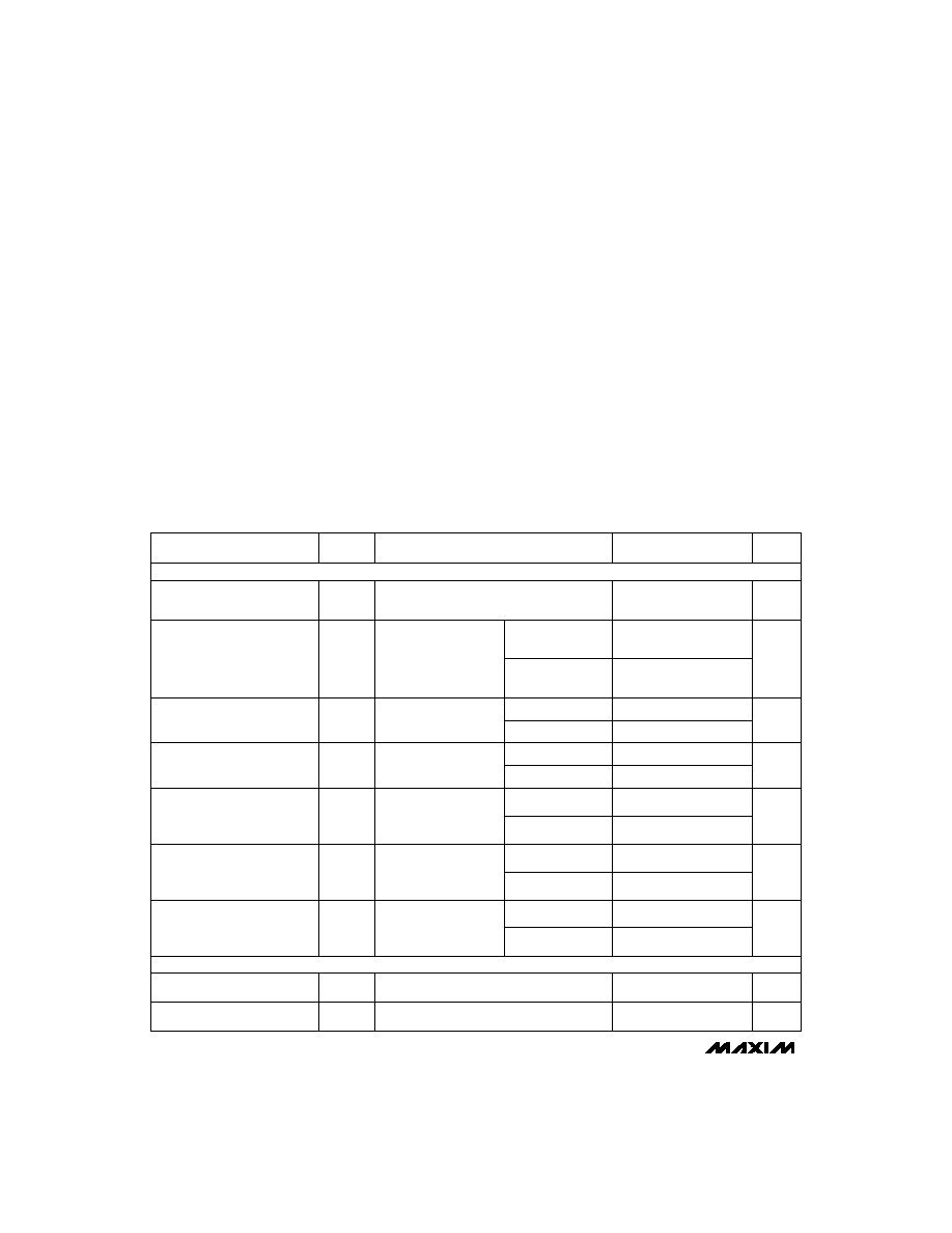
ABSOLUTE MAXIMUM RATINGS
ELECTRICAL CHARACTERISTICS--Dual Supplies
(V+ = 15V, V- = -15V, VL = 5V, GND = 0V, V
INH
= 2.4V, V
INL
= 0.8V, T
A
= T
MIN
to T
MAX
, unless otherwise noted.)
Stresses beyond those listed under "Absolute Maximum Ratings" may cause permanent damage to the device. These are stress ratings only, and functional
operation of the device at these or any other conditions beyond those indicated in the operational sections of the specifications is not implied. Exposure to
absolute maximum rating conditions for extended periods may affect device reliability.
PARAMETER
SYMBOL
UNITS
R
ON
15
9
R
ON
2
100
-0.50
0.01
0.50
NC_ or NO_ Leakage Current
I
NO_
,
I
NC
-4
4
nA
-0.50
0.01
0.50
COM_ Off Leakage Current
I
NO
,
I
NC
-4
4
nA
Analog-Signal Range
-15
15
V
On Resistance
R
ON
50
85
-0.50
0.08
0.50
COM_, NC_ or NO_ On
Leakage Current
-6
6
nA
I
INH
-0.5
-0.00001
0.5
µA
I
INL
-0.5
-0.00001
0.5
µA
CONDITIONS
(Note 3)
Voltage Referenced to V-
V+........................................................................................44V
GND ....................................................................................25V
VL ..................................................(GND - 0.3V) to (V+ + 0.3V)
IN_, COM_, NO_, or NC_ ..........(V- - 2V) to (V+ + 2V) or 30mA
................................................................
(whichever occurs first)
Continuous Current (any terminal) ......................................30mA
Peak Current COM_, NO_, or NC_
(pulsed at 1ms, 10% duty cycle max) ...........................100mA
ESD ....................................................................................2000V
Continuous Power Dissipation (T
A
= +70°C) (Note 1)
Plastic DIP (derate 10.53mW/°C above +70°C.............842mW
Narrow SO (derate 8.70mW/°C above +70°C) .............696mW
Operating Temperature Ranges:
MAX36_C_ _ ........................................................0°C to +70°C
MAX36_E_ _......................................................-40°C to +85°C
Storage Temperature Range .............................-65°C to +150°C
Lead Temperature (soldering, 10sec) .............................+300°C
Note 1:
All leads are soldered or welded to PC board.
V
COM_
,
V
NO_
,
V
NC
T
A
= +25°C
COM_ to NO_ or NC,
I
COM
= -10mA,
V
COM
= 8.5V or -8.5V,
V+ = 13.5V, V- = -13.5V
T
A
= T
MIN
to T
MAX
On Resistance Match
Between Channels (Note 4)
T
A
= +25°C
4
T
A
= T
MIN
to T
MAX
I
COM
= -10mA,
V
COM
= 10V or -10V,
V+ = 15V, V- = -15V
T
A
= +25°C
T
A
= T
MIN
to T
MAX
On Resistance Flatness (Note 4)
I
COM
= -10mA,
V
COM
= 5V or -5V,
V+ = 15V, V- = -15V
T
A
= +25°C
T
A
= T
MIN
to T
MAX
NO_ or NC_ terminal,
V
COM
= ±15.5V,
V
NO
or V
NC
=
+15.5V,
V+ = 16.5V, V- = -16.5V
I
COM
or
I
NO
, I
NC
Input Current with
Input Voltage High
Input Current with
Input Voltage Low
T
A
= +25°C
T
A
= T
MIN
to T
MAX
T
A
= +25°C
T
A
= T
MIN
to T
MAX
V
IN_
= 2.4V, all others = 0.8V
V
IN_
= 0.8V, all others = 2.4V
COM_ terminal,
V
NO
or V
NC
= ±15.5V,
V
COM
=
+15.5V,
V+ = 16.5V, V- = -16.5V
COM_ to NC_ or NO_
V
COM
= ±15.5V,
V
NO
or V
NC
= ±15.5V,
V+ = 16.5V, V- = -16.5V
MIN
TYP
MAX
(Note 2)
ANALOG
INPUT

MAX364/MAX365
Precision, Quad, SPST Analog Switches
_______________________________________________________________________________________
3
ELECTRICAL CHARACTERISTICS--Dual Supplies (continued)
(V+ = 15V, V- = -15V, VL = 5V, GND = 0V, V
INH
= 2.4V, V
INL
= 0.8V, T
A
= T
MIN
to T
MAX
, unless otherwise noted.)
PARAMETER
T
A
= +25°C
SYMBOL
MIN
TYP
MAX
(Note 2)
T
A
= T
MIN
to T
MAX
UNITS
T
A
= +25°C
I-
-5
5
µA
Negative Supply Current
T
A
= T
MIN
to T
MAX
-1
-0.0001
1
Positive Supply Current
I+
-1
0.001
1
T
A
= +25°C
T
A
= +25°C
-1
0.001
1
Logic Supply Current
I
L
-5
5
µA
Turn-On Time
V
NO
or V
NC
= ±10V, Figure 2
t
ON
-1
-0.0001
1
150
250
Ground Current
ns
I
GND
-5
5
µA
Power-Supply Range
V+, V-
±4.5
±20.0
V
T
A
= T
MIN
to T
MAX
CONDITIONS
All channels on or off,
V
IN
= 0V or 5V,
V+ = 16.5V, V- = -16.5V
-5
5
All channels on or off,
V
IN
= 0V or 5V,
V+ = 16.5V, V- = -16.5V
All channels on or off,
V
IN
= 0V or 5V,
V+ = 16.5V, V- = -16.5V
µA
T
A
= T
MIN
to T
MAX
All channels on or off,
V
IN
= 0V or 5V,
V+ = 16.5V, V- = -16.5V
T
A
= +25°C
T
A
= +25°C
Turn-Off Time
MAX364, V
NO
or V
NC
= ±10V,
Figure 2
90
120
ns
T
A
= +25°C
MAX365, V
NO
or V
NC
= ±10V,
Figure 2
t
OFF
110
170
ns
T
A
= +25°C
Off Isolation (Note 5)
OIRR
60
dB
T
A
= +25°C
Charge Injection
Q
5
10
pC
T
A
= +25°C
Crosstalk (Note 6)
100
dB
T
A
= +25°C
NC_ or NO_ Off
Capacitance
f = 1MHz, Figure 6
C
(OFF)
4
pF
T
A
= +25°C
COM_ Off Capacitance
f = 1MHz, Figure 6
C
COM(OFF)
4
pF
T
A
= +25°C
f = 1MHz, Figure 6
16
pF
C
L
= 1nF, V
GEN
= 0V,
R
GEN
= 0
, Figure 3
R
L
= 50
, C
L
= 5pF,
f = 1MHz, Figure 4
Channel-On Capacitance
C
COM(ON)
RL - 50
, CL = 5pF,
f = 1MHz, Figure 5
SUPPLY
DYNAMIC

MAX364/MAX365
Precision, Quad, SPST Analog Switches
4
_______________________________________________________________________________________
ELECTRICAL CHARACTERISTICS--Single Supply
(V+ = 12V, V- = 0V, VL = 5V, GND = 0V, V
INH
= 2.4V, V
INL
= 0.8V, T
A
= T
MIN
to T
MAX
, unless otherwise noted.)
PARAMETER
SYMBOL
MIN
TYP
MAX
(Note 2)
UNITS
T
A
= +25°C
100
160
T
A
= T
MIN
to T
MAX
-1
0.001
1
Power-Supply Current
I+
-5
5
µA
Analog Signal Range
0
12
V
CONDITIONS
All channels on or off,
V
IN
= 0V or 5V
(Note 3)
T
A
= +25°C
T
A
= T
MIN
to T
MAX
-1
-0.0001
1
Negative Supply Current
I-
-5
5
µA
All channels on or off,
V
IN
= 0V or 5V
T
A
= +25°C
T
A
= T
MIN
to T
MAX
-1
-0.0001
1
Ground Current
I
GND
-5
5
µA
All channels on or off,
V
IN
= 0V or 5V
T
A
= +25°C
T
A
= T
MIN
to T
MAX
-1
0.001
1
Logic Supply Current
I
L
-5
5
µA
All channels on or off,
V
IN
= 0V or 5V
V
COM_
,
V
NO_
,
V
NC_
V
10.8
24.0
V+, V-
Power-Supply Range
T
A
= +25°C
200
T
A
= T
MIN
to T
MAX
R
ON
On Resistance
COM_ to NO_ or NC_,
I
NC
or I
NO
= -10mA,
VL = 5.25V,
V
COM
= 3V, 8V,
V+ = 10.8V
T
A
= +25°C
300
400
V
NC
or V
NO
= 8V, Figure 2
ns
t
ON
Turn-On Time
T
A
= +25°C
60
200
V
NC
or V
NO
= 8V, Figure 2
ns
t
OFF
Turn-Off Time
T
A
= +25°C
5
10
pC
Q
Charge Injection
C
L
= 1nF, V
GEN
= 0V,
R
GEN
= 0
, Figure 3
Note 2:
The algebraic convention, where the most negative value is a minimum and the most positive value a maximum, is used in
this data sheet.
Note 3:
Guaranteed by design.
Note 4:
On resistance match between channels and flatness are guaranteed only with bipolar-supply operation.
Note 5:
See Figure 2. Off Isolation = 20 log
10
, V
COM
= output, V
NO
or V
NC
= input to off switch.
Note 6:
Between any two switches. See Figure 5.
VCOM
VNC or VNO
ANALOG
DYNAMIC
SUPPLY

MAX364/MAX365
Precision, Quad, SPST Analog Switches
_______________________________________________________________________________________
5
__________________________________________Typical Operating Characteristics
(T
A
= +25°C, unless otherwise noted.)
ON LEAKAGE CURRENTS
I
COM (nA)
-2
-1
0
1
2
-15
0
15
VNC, VNO, VCOM (V)
IS(ON) + ID(ON)
T
A
= +125°C
T
A
= +85°C
V+ = 15V
V- = -15V
MAX7864/5-1
OFF LEAKAGE CURRENTS
I NC
or I
NO
(nA)
-1
0
1
-15
0
15
VNC, VNO, VCOM (V)
T
A
= +85°C
T
A
= +125°C
V+ = 15V
V- = -15V
MAX7864/5-2
SWITCHING THRESHOLD vs.
BIPOLAR SUPPLY VOLTAGE
V
IN
(V)
0
0.5
1.5
2.0
2.5
3.0
3.5
±5
±10
±15
±20
BIPOLAR SUPPLY VOLTAGE (V)
MAX7864/5-3
ON RESISTANCE vs. VCOM AND
UNIPOLAR SUPPLY VOLTAGE
0
25
50
75
100
125
0
5
10
15
20
VCOM (V)
R
ON
(
)
MAX7864/5-4
V+ = 10V
V+ = 15V
V+ = 20V
150
ON RESISTANCE vs. VCOM, UNIPOLAR
SUPPLY VOLTAGE AND TEMPERATURE
0
25
50
75
100
125
150
R
ON
(
)
0
4
8
12
VCOM (V)
MAX7864/5-7
T
A
= +125°C
T
A
= +25°C
T
A
= -55°C
V+ = 12V
V- = 0V
ON RESISTANCE vs. VCOM AND
BIPOLAR SUPPLY VOLTAGE
R
ON
(
)
30
60
90
120
-20
-10
0
10
20
VCOM (V)
0
MAX7864/5-5
±5V
±10V
±15V
±20V
ON RESISTANCE vs. VCOM,
BIPOLAR SUPPLY VOLTAGE AND TEMPERATURE
R
ON
(
)
0
20
40
60
80
100
-14
-7
0
7
14
VCOM (V)
MAX7864/5-6
T
A
= +125°C
T
A
= -55°C
T
A
= +25°C
V+ = 15V, V- = -15V
SWITCHING TIME vs.
BIPOLAR SUPPLY VOLTAGE
TIME (ns)
0
40
80
120
160
±5
±10
±15
±20
BIPOLAR SUPPLY VOLTAGE (V)
MAX7864/5-8
t ON
t OFF
SWITCHING TIMES vs.
UNIPOLAR SUPPLY VOLTAGE
TIME (ns)
0
50
100
150
200
10
15
20
24
UNIPOLAR SUPPLY VOLTAGE (V)
V- = 0V
MAX7864/5-9
t ON
t OFF