General Description
The MAX3524 evaluation kit (EV kit) enables RF evalua-
tion of the MAX3524 low-noise, high-linearity broad-
band amplifier and the closed-loop DC gain of the
operational amplifier (op amp) without any additional
support circuitry. The MAX3524 EV kit is assembled
with the MAX3524 and incorporates input and output
components that facilitate testing from 44MHz to
880MHz. The EV kit provides 50
SMA connectors for
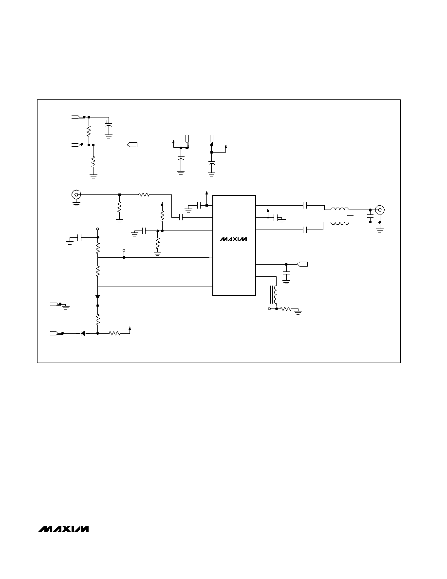
the RF input and output signals. Figure 1 shows the
MAX3524 EV kit schematic diagram. For more informa-
tion about the MAX3524, consult the MAX3524 data
sheet.
Features
o Easy Evaluation of the MAX3524
o +4.75V to +5.25V Single-Supply Operation
o RF Input and Output Matched to 50
o SMA Connectors at RF Signal Ports
o 50 to 75 Minimum Loss Pad at the Input
Evaluates: MAX3524
MAX3524 Evaluation Kit
________________________________________________________________ Maxim Integrated Products
1
19-1881; Rev 0; 12/00
Component List
Ordering Information
PART
TEMP RANGE
IC-PACKAGE
MAX3524EVKIT
-40
°C to +85°C
10 µMAX-EP
DESIGNATION
QTY
DESCRIPTION
C1
1
47pF
±5% ceramic capacitor
(0603)
Murata GRM39COG470J050A
C2, C14
Not installed
C3, C19, C20
3
10
µF, 16V ±10% tantalum
capacitors
AVX TAJC106K016
C10, C11, C12,
C13, C15, C16
6
0.1
µF ±10% ceramic capacitors
(0603)
Murata GRM39X7R104K016A
D1, D2
2
Diodes
Central Semiconductor
CMDSH-3 (SOD323)
J1, J7
2
SMA edge mount connectors
EF Johnson 142-0701-801
J2, J3, J4, J5,
J6, J9, TP1,
TP4, TP5
9
Test points
L5
1
680nH inductor
Coilcraft 1206CS-681XJBC
R1
1
43.2
±1% resistor (0603)
Kamaya RMC16-43R2FT
DESIGNATION
QTY
DESCRIPTION
R2
1
86.6
±1% resistor (0603)
Kamaya RMC16-86R6FT
R3, R7
Not installed
R4
1
49.9k
±1% resistor (0603)
Kamaya RMC16-4992FT
R5, R6, R10,
R11
4
3k
±5% resistors (0603)
Kamaya RMC16-302JB
R9
1
100
±5% resistor (0603)
Kamaya RMC16-101JB
R12
1
6.19
±1% resistor (0603)
RMC16-6R20FT
T2
1
Balun transformer
M/A COM ETC1-1-13
U1
1
MAX3524EUB, 10-pin
µMAX-EP
NOTE: U1 has an exposed
paddle requiring soldering to the
circuit board to insure proper
function of the part.
None
1
MAX3524 EV kit data sheet
None
1
MAX3524 Rev C EV kit circuit
board
For price, delivery, and to place orders, please contact Maxim Distribution at 1-888-629-4642,
or visit Maxim's website at www.maxim-ic.com.
Evaluates: MAX3524
MAX3524 Evaluation Kit
2
_______________________________________________________________________________________
Quick Start
The MAX3524 EV kit is fully assembled and factory test-
ed. Follow the instructions in the Connections and
Setup section for proper device evaluation.
Connections and Setup
This section provides a step-by-step guide to setting up
the MAX3524 EV kit and testing the broadband LNA. Do
not apply DC power or RF signals until all connec-
tions are made.
Broadband Low Noise Amplifier
Note: The input to the LNA is preceded by a minimum
loss pad that transforms the source impedance from
50
to 75. The insertion loss of this is pad is 5.7dB.
1) Connect a DC supply preset to +5V (through an
ammeter, if desired) to the EV kit's V
CC
(J9) and
GND (J6) terminals. Do not turn on the supply.
2) Perform a full two-port calibration on a network ana-
lyzer at a power level of -25dBm. Refer to the net-
work analyzer's operating manual for detailed
instructions.
3) Connect port 1 and port 2 of a network analyzer to
the LNAIN SMA connector (J1) and LNAOUT SMA
connector (J7), respectively.
4) Turn on the DC supply. The supply current should
read approximately 85mA (if using an ammeter).
Measure DC voltage between J9 and J6 to ensure 5V
operation. Adjust power supply output as needed.
5) The network analyzer display should indicate a typi-
cal gain of 4.25dB at 44MHz. The MAX3524 EV kit
utilizes a 50
to 75 pad. The insertion loss of this
pad is approximately 5.7dB. The actual gain of the
MAX3524 when driven by a 75
source is:
Measured Gain + 5.72dB
(The MAX3524 data sheet specifies voltage gain with a
3k
load. This typically results in a voltage gain of
15dB.)
Checking Noise Figure
Noise figure measurements are sensitive to board and
lab setup losses and parasitics. There are many tech-
niques and precautions for measuring a low-noise fig-
ure. Detailed explanation of these items goes beyond
the scope of this document. For more information on
how to perform this level of noise-figure measurement,
refer to the noise-figure meter operating manual, as well
as to Hewlett Packard application note #57-2, Noise
Figure Measurement Accuracy. The EV kit board con-
sists of a 50
to 75 pad at the input of the amplifier,
which introduces a loss of 5.72dB. To obtain the correct
noise figure of the MAX3524, subtract 5.72dB from the
measured noise figure.
Closed-Loop Gain of Op Amp
1) Connect a DC supply preset to +5V (through an
ammeter, if desired) to the EV kit's V
CC
(J9) and
GND (J6) terminals. Do not turn on the supply.
2) Connect a second DC supply preset to +2V to the
EV kit's terminal J2 and GND (J6) terminals.
3) Turn on the DC supplies.
4) Measure the output of the op amp at TP4 (Test Point
4) using the voltmeter. The voltmeter should display
approximately +2V, taking into account the input
resistor voltage-divider (1/2 and closed-loop gain
+2) of the op amp.
PC Board Layout Considerations
The MAX3524 EV kit can serve as a board layout guide.
Keep PC board trace lengths as short as possible to
minimize parasitics. Long PC board traces at the input
and output of the MAX3524 can degrade gain flatness.
Keep decoupling capacitors as close to the device as
possible, with a low inductance connection to the
ground plane.
Two Power Supplies or a
Dual Voltage Power Supply
One supply capable of
providing at least 200mA at
+4.75V to +5.25V to bias
the RF amplifier and the op
amp. The other supply to
test the closed-loop gain of
the op amp.
Network Analyzer
HP8753D or equivalent for
measuring RF power gain.
Cables (50
)
Two 50
cables with SMA
connectors.
Voltmeter
To measure op amp output.
Ammeter (optional)
For measuring supply
current.
Noise Figure Meter (optional)
HP8970B or equivalent for
measuring the noise figure
of the RF amplifier.
Recommended Test Equipment
Evaluates: MAX3524
MAX3524 Evaluation Kit
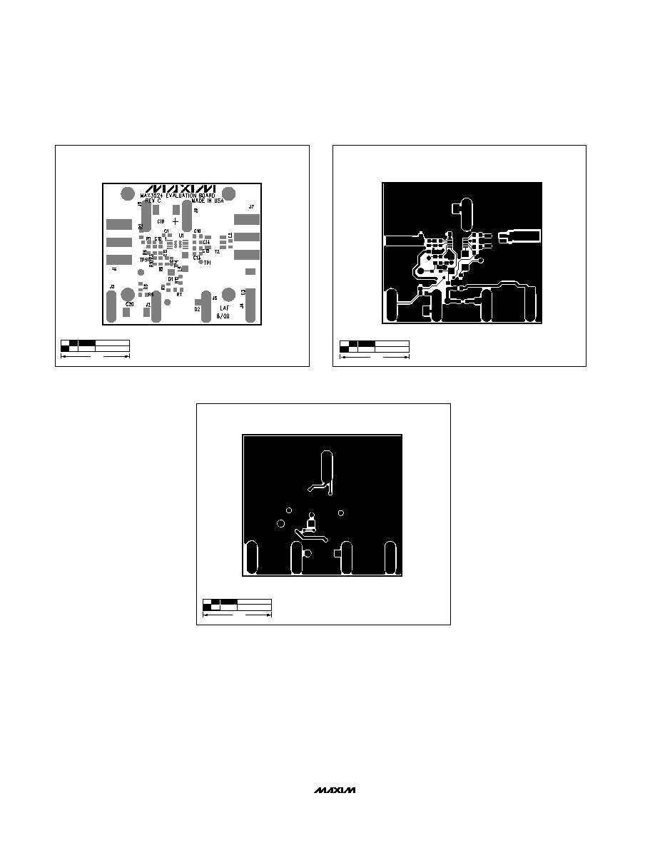
Figure 2. MAX3524 EV Kit Component Placement Guide--
Component Side
Figure 3. MAX3524 EV Kit PC Board Layout--Component Side
Figure 4. MAX3524 EV Kit PC Board Layout--Ground Side
1.0"
1.0"
1.0"
Maxim cannot assume responsibility for use of any circuitry other than circuitry entirely embodied in a Maxim product. No circuit patent licenses are
implied. Maxim reserves the right to change the circuitry and specifications without notice at any time.
Maxim Integrated Products, 120 San Gabriel Drive, Sunnyvale, CA 94086 408-737-7600 _____________________ 5
© 2000 Maxim Integrated Products
Printed USA
is a registered trademark of Maxim Integrated Products.