General Description
The MAX3421E USB peripheral/host controller contains
the digital logic and analog circuitry necessary to
implement a full-speed USB peripheral or a full-/low-
speed host compliant to USB specification rev 2.0. A
built-in transceiver features ±15kV ESD protection and
programmable USB connect and disconnect. An inter-
nal serial interface engine (SIE) handles low-level USB
protocol details such as error checking and bus retries.
The MAX3421E operates using a register set accessed
by an SPITM interface that operates up to 26MHz. Any
SPI master (microprocessor, ASIC, DSP, etc.) can add
USB peripheral or host functionality using the simple 3-
or 4-wire SPI interface.
The MAX3421E makes the vast collection of USB
peripherals available to any microprocessor, ASIC, or
DSP when it operates as a USB host. For point-to-point
solutions, for example, a USB keyboard or mouse inter-
faced to an embedded system, the firmware that oper-
ates the MAX3421E can be simple since only a
targeted device is supported.
Internal level translators allow the SPI interface to run at
a system voltage between 1.4V and 3.6V. USB-timed
operations are done inside the MAX3421E with inter-
rupts provided at completion so an SPI master does not
need timers to meet USB timing requirements. The
MAX3421E includes eight general-purpose inputs and
outputs so any microprocessor that uses I/O pins to
implement the SPI interface can reclaim the I/O pins
and gain additional ones.
The MAX3421E operates over the extended -40°C to
+85°C temperature range and is available in a 32-pin
TQFP package (5mm x 5mm) and a 32-pin TQFN pack-
age (5mm x 5mm).
Applications
Features
Microprocessor-Independent USB Solution
Software Compatible with the MAX3420E USB
Peripheral Controller with SPI Interface
Complies with USB Specification Revision 2.0
(Full-Speed 12Mbps Peripheral, Full-/Low-Speed
12Mbps/1.5Mbps Host)
Integrated USB Transceiver
Firmware/Hardware Control of an Internal D+
Pullup Resistor (Peripheral Mode) and D+/D-
Pulldown Resistors (Host Mode)
Programmable 3- or 4-Wire, 26MHz SPI Interface
Level Translators and V
L
Input Allow Independent
System Interface Voltage
Internal Comparator Detects V
BUS
for Self-
Powered Peripheral Applications
ESD Protection on D+, D-, and VBCOMP
Interrupt Output Pin (Level- or Programmable-
Edge) Allows Polled or Interrupt-Driven SPI
Interface
Eight General-Purpose Inputs and Eight General-
Purpose Outputs
Interrupt Signal for General-Purpose Input Pins,
Programmable Edge Polarity
Intelligent USB SIE
Automatically Handles USB Flow Control and
Double Buffering
Handles Low-Level USB Signaling Details
Contains Timers for USB Time-Sensitive
Operations so SPI Master Does Not Need to Time
Events
Space-Saving Lead-Free TQFP and TQFN
Packages (5mm x 5mm)
MAX3421E
USB Peripheral/Host Controller
with SPI Interface
________________________________________________________________ Maxim Integrated Products
1
19-3953; Rev 0; 2/06
For pricing, delivery, and ordering information, please contact Maxim/Dallas Direct! at
1-888-629-4642, or visit Maxim's website at www.maxim-ic.com.
Embedded Systems
Medical Devices
Microprocessors and
DSPs
Custom USB Devices
Cameras
Desktop Routers
PLCs
Set-Top Boxes
PDAs
MP3 Players
Instrumentation
PART
TEMP RANGE
PIN-
PACKAGE
PKG CODE
M AX 3421E E H J+ - 40°C to + 85°C
32 TQFP
H 32- 1
M AX 3421E E TG+ * - 40°C to + 85°C 32
TQFN
- E P **
T3255- 4
Ordering Information
*Future product--contact factory for availability.
**EP = Exposed paddle, connected to ground.
SPI is a trademark of Motorola, Inc.

MAX3421E
Features in Host Operation
Eleven Registers (R21R31) are Added to the
MAX3420E Register Set to Control Host Operation
Host Controller Operates at Full Speed or Low
Speed
FIFOS
SNDFIFO: Send FIFO, Double-Buffered 64-Byte
RCVFIFO: Receive FIFO, Double-Buffered 64-Byte
Handles DATA0/DATA1 Toggle Generation and
Checking
Performs Error Checking for All Transfers
Automatically Generates SOF (Full-Speed)/EOP
(Low-Speed) at 1ms Intervals
Automatically Synchronizes Host Transfers with
Beginning of Frame (SOF/EOP)
Reports Results of Host Requests
Supports USB Hubs
Supports ISOCHRONOUS Transfers
Simple Programming
SIE Automatically Generates Periodic SOF
(Full-Speed) or EOP (Low-Speed) Frame
Markers
SPI Master Loads Data, Sets Function Address,
Endpoint, and Transfer Type, and Initiates the
Transfer
MAX3421E Responds with an Interrupt and
Result Code Indicating Peripheral Response
Transfer Request Can be Loaded Any Time
SIE Synchronizes with Frame Markers
For Multipacket Transfers, the SIE
Automatically Maintains and Checks the
Data Toggles
Features in Peripheral Operation
Built-In Endpoint FIFOS
EP0: CONTROL (64 bytes)
EP1: OUT, Bulk or Interrupt, 2 x 64 Bytes
(Double-Buffered)
EP2: IN, Bulk or Interrupt, 2 x 64 Bytes (Double-
Buffered)
EP3: IN, Bulk or Interrupt (64 Bytes)
Double-Buffered Data Endpoints Increase
Throughput by Allowing the SPI Master to
Transfer Data Concurrent with USB Transfers
SETUP Data Has its Own 8-Byte FIFO, Simplifying
Firmware
USB Peripheral/Host Controller
with SPI Interface
2
_______________________________________________________________________________________
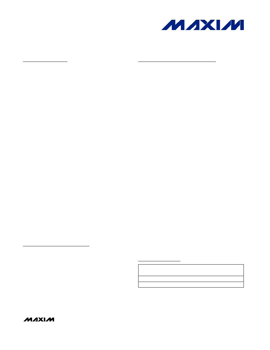
The MAX3421E connects to any microprocessor (µP)
using 3 or 4 interface pins (Figure 1). On a simple
microprocessor without SPI hardware, these can be
bit-banged general-purpose I/O pins. Eight GPIN and
eight GPOUT pins on the MAX3421E more than
replace the µP pins necessary to implement the inter-
face. Although the MAX3421E SPI hardware includes
separate data-in (MOSI, master-out, slave-in) and data-
out (MISO, master-in, slave-out) pins, the SPI interface
can also be configured for the MOSI pin to carry bidi-
rectional data, saving an interface pin. This is referred
to as half-duplex mode.
Typical Application Circuits
3.3V
REGULATOR
SPI
3, 4
INT
USB
µP
MAX3421E
Figure 1. The MAX3421E Connects to Any Microprocessor
Using 3 or 4 Interface Pins
MAX3421E
USB Peripheral/Host Controller
with SPI Interface
_______________________________________________________________________________________
3
3.3V
REGULATOR
POWER RAIL
ASIC,
DSP,
ETC.
SPI
3, 4
INT
MAX3421E
USB
Figure 2. The MAX3421E Connected to a Large Chip
3.3V
REGULATOR
MISO
LOCAL
GND
LOCAL
POWER
INT
MAX3421E
SCLK
MOSI
SS
MICRO
ASIC
DSP
I
S
O
L
A
T
O
R
S
USB
Figure 3. Optical Isolation of USB Using the MAX3421E
MICRO,
ASIC,
DSP
USB
PERIPHERAL
USB
"A"
USB
"B"
V
BUS
SWITCH
FAULT
5V
SPI
3, 4
INT
V
BUS
D+
D-
GND
V
BUS
POWER
ON/OFF
3.3V
REGULATOR
MAX3421E
Figure 4. The MAX3421E in an Embedded Host Application
Two MAX3421E features make it easy to connect to
large, fast chips such as ASICs and DSPs (Figure 2).
First, the SPI interface can be clocked up to 26MHz.
Second, the V
L
pin and internal level translators allow
running the system interface at a lower voltage than
the 3.3V required for V
CC
.
The MAX3421E provides an ideal method for electrically
isolating a USB interface (Figure 3). USB employs flow
control in which the MAX3421E automatically answers
host requests with a NAK handshake, until the micro-
processor completes its data-transfer operations over
the SPI port. This means that the SPI interface can run
at any frequency up to 26MHz. Therefore, the designer
is free to choose the interface operating frequency and
to make opto-isolator choices optimized for cost or per-
formance.
Figure 4 shows a block diagram for a system in which
the MAX3421E operates as a USB host. A USB host
supplies 5V power to the V
BUS
pin of the USB "A" con-
nector to power USB peripherals. A system that pro-
vides power to an external peripheral should use
protection circuitry on the power pin to prevent an
external overcurrent situation from damaging the sys-
tem. A V
BUS
switch, such as the MAX4789, provides
power control plus two additional features: it limits the
current delivered to the peripheral (for example to
200mA), and it indicates a fault (overcurrent) condition
to the SPI controller. Maxim offers a variety of V
BUS
switches with various current limits and features.
Consult the Maxim website for details.
A 3.3V regulator (for example, the MAX6349TL) powers
the MAX3421E, and optionally the system controller. If
the system controller operates with a lower voltage, the
MAX3421E SPI and I/O interface can run at the lower
voltage by connecting the system voltage (for exam-
ple, 2.5V or 1.8V) to the MAX3421E V
L
pin.
Typical Application Circuits (continued)

MAX3421E
USB Peripheral/Host Controller
with SPI Interface
4
_______________________________________________________________________________________
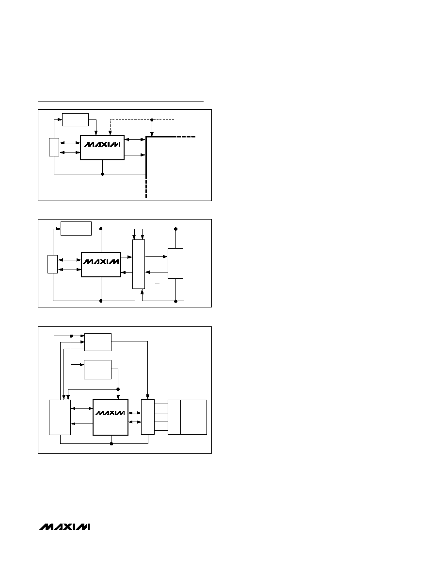
Functional Diagram
GPIN0
1V TO 3V
VBCOMP
D-
D+
V
CC
R
GPIN
VBUS
COMP
SS
MISO
SCLK
INT
SPI SLAVE
INTERFACE
USB SIE
(SERIAL-
INTERFACE
ENGINE)
FULL-SPEED/
LOW-SPEED
USB
TRANSCEIVER
RESET
LOGIC
1.5k
INTERNAL
POR
RES
XI
XO
POWER
DOWN
OSC
AND
4x PLL
48MHz
ESD
PROTECTION
ESD
PROTECTION
GPX
OPERATE
SOF
BUSACT/
INIRQ
MUX
0
1
2
3
MOSI
VBUS_DET
ENDPOINT
BUFFERS
MAX3421E
GND
GPIN1
GPIN2
GPIN3
GPIN4
GPIN5
GPIN6
GPIN7
GPOUT0
GPOUT1
GPOUT2
GPOUT3
GPOUT4
GPOUT5
GPOUT6
GPOUT7
V
L
R
IN
15k
15k

MAX3421E
USB Peripheral/Host Controller
with SPI Interface
_______________________________________________________________________________________
5
Pin Description
PIN
NAME
INPUT/
OUTPUT
FUNCTION
1
GPIN7
Input
General-Purpose Input. GPIN7GPIN0 are connected to V
L
with internal pullup resistors.
GPIN7GPIN0 logic levels are referenced to the voltage on V
L
.
2
V
L
Input
Level-Translator Voltage Input. Connect V
L
to the system's 1.4V to 3.6V logic-level power
supply. Bypass V
L
to ground with a 0.1µF capacitor as close to V
L
as possible.
3, 19
GND
Input
Ground
4
GPOUT0
5
GPOUT1
6
GPOUT2
7
GPOUT3
8
GPOUT4
9
GPOUT5
10
GPOUT6
11
GPOUT7
Output
General-Purpose Push-Pull Outputs. GPOUT7GPOUT0 logic levels are referenced to the
voltage on V
L
.
12
RES
Input
Device Reset. Drive
RES low to clear all of the internal registers except for PINCTL (R17),
USBCTL (R15), and SPI logic. The logic level is referenced to the voltage on V
L
. (See the
Device Reset section for a description of resets available on the MAX3421E.)
13
SCLK
Input
SPI Serial-Clock Input. An external SPI master supplies SCLK with frequencies up to 26MHz.
The logic level is referenced to the voltage on V
L
. Data is clocked into the SPI slave interface
on the rising edge of SCLK. Data is clocked out of the SPI slave interface on the falling edge of
SCLK.
14
SS
Input
SPI Slave Select Input. The
SS logic level is referenced to the voltage on V
L
. When
SS is driven
high, the SPI slave interface is not selected, the MISO pin is high impedance, and SCLK
transitions are ignored. An SPI transfer begins with a high-to-low
SS transition and ends with a
low-to-high
SS transition.
15
MISO
Output
SPI Serial-Data Output (Master-In Slave-Out). MISO is a push-pull output. MISO is tri-stated in
half-duplex mode or when
SS = 1. The MISO logic level is referenced to the voltage on V
L
.
16
MOSI
Input or
Input/
Output
SPI Serial-Data Input (Master-Out Slave-In). The logic level on MOSI is referenced to the
voltage on V
L
. MOSI can also be configured as a bidirectional MOSI/MISO input and output.
(See Figure 15.)
17
GPX
Output
General-Purpose Multiplexed Push-Pull Output. The internal MAX3421E signal that appears on
GPX is programmable by writing to the GPXB and GPXA bits of the PINCTL (R17) register and
the SEPIRQ bit of the MODE (R27) register. GPX indicates one of five signals (see the GPX
section).
18
INT
Output
Interrupt Output. In edge mode, the logic level on INT is referenced to the voltage on V
L
and is
a push-pull output with programmable polarity. In level mode, INT is open-drain and active low.
Set the IE bit in the CPUCTL (R16) register to enable INT.
20
D-
Input/
Output
USB D- Signal. Connect D- to a USB connector through a 33
±1% series resistor. A
switchable 15k
D- pulldown resistor is internal to the device.