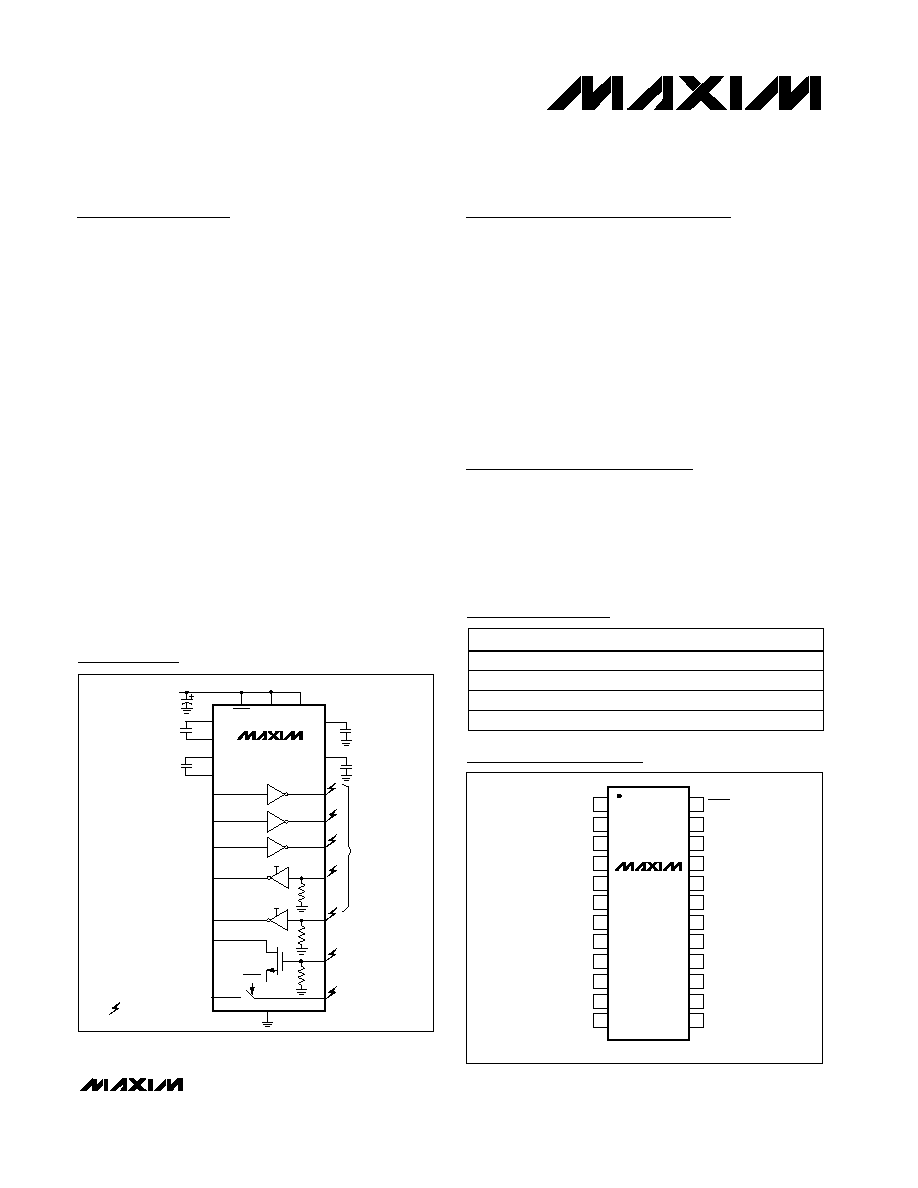
General Description
The MAX3388E/MAX3389E are 2.5V-powered EIA/TIA-
232 and V.28/V.24 communications interfaces with low
power requirements, high data-rate capabilities, and
enhanced electrostatic discharge (ESD) protection. The
MAX3388E/MAX3389E have two receivers and three
transmitters. All RS-232 inputs and outputs are protected
to ±15kV using the IEC 1000-4-2 Air-Gap Discharge
method, ±8kV using the IEC 1000-4-2 Contact Discharge
method, and ±15kV using the Human Body Model.
In addition to the traditional RS-232 I/O, these devices have
dedicated logic-level I/O pins for additional device-to-
device handshaking. During shutdown the logic-level I/O
pins are active for the MAX3389E. An internal 62
switch is
provided to switch power to external circuitry or modules.
A proprietary low-dropout transmitter output stage
enables RS-232 compatible performance from a +2.35V
to +3.0V supply with a dual charge pump. The charge
pump requires only four small 0.1µF capacitors for oper-
ation from a +2.5V supply. The MAX3388E/MAX3389E
are capable of running at data rates up to 460kbps while
maintaining RS-232-compatible output levels.
The MAX3388E/MAX3389E have a unique V
L
pin that
allows interoperation in mixed-logic voltage systems.
Both input and output logic levels are pin programma-
ble through the V
L
pin. The MAX3388E/MAX3389E are
available in a space-saving TSSOP package.
Features
o V
L
Pin for Compatibility with Mixed-Voltage
Systems
o Additional I/O for Hot-Sync Applications
o ±15kV ESD Protection on Rx Inputs, Tx Outputs,
LIN, and SWIN
o Low 300µA Supply Current
o Guaranteed 460kbps Data Rate
o 1µA Low-Power Shutdown
o Integrated Switch for Powering Remote Circuitry
o Flow-Through Pinout
o L
OUT
Active During Shutdown (MAX3389E)
Applications
Subnotebook/Palmtop Computers
PDAs and PDA Cradles
Cell Phone Data Cables
Battery-Powered Equipment
Hand-Held Equipment
Peripherals
MAX3388E/MAX3389E
2.5V, ±15kV ESD-Protected RS-232
Transceivers for PDAs and Cell Phones
________________________________________________________________ Maxim Integrated Products
1
24
23
22
21
20
19
18
17
1
2
3
4
5
6
7
8
SHDN
V
CC
GND
T1OUT
C2+
C1-
V+
C1+
TOP VIEW
T2OUT
T3OUT
R1IN
R2IN
T2IN
T1IN
V-
C2-
16
15
14
13
9
10
11
12
LIN
SWIN
V
L
R1OUT
R2OUT
SWOUT
LOUT
T3IN
TSSOP
MAX3388E
MAX3389E
Typical Operating Circuit
19-1845; Rev 1; 9/01
Pin Configuration
Ordering Information
PART
TEMP. RANGE
PIN-PACKAGE
MAX3388ECUG
0°C to +70°C
24 TSSOP
MAX3388EEUG
-40°C to +85°C
24 TSSOP
MAX3389ECUG
0°C to +70°C
24 TSSOP
MAX3389EEUG
-40°C to +85°C
24 TSSOP
MAX3388E
MAX3389E
R2OUT
12
R1OUT
V
L
13
R2IN
17
GND
22
RS-232
I/O
T2IN
8
T1IN
7
C2-
5
C2+
4
C1-
3
C1+
1
R1IN
18
T2OUT
20
T1OUT
21
V-
6
V+
2
V
CC
V
L
14
23
C1
0.1
µF
C2
0.1
µF
C
BYPASS
+2.5V
T3IN
9
T3OUT
19
5k
5k
C3
0.1
µF
C4
0.1
µF
V
L
24
SHDN
SWIN 15
16
LIN
30k
11
SWOUT
SHDN
10 LOUT
=
±15kV ESD PROTECTION
Covered by U.S Patent numbers 4,636,930; 4,679,134;
4,777,577; 4,797,899; 4,809,152; 4,897,774; 4,999,761.
For pricing, delivery, and ordering information, please contact Maxim/Dallas Direct! at
1-888-629-4642, or visit Maxim's website at www.maxim-ic.com.
MAX3388E/MAX3389E
2.5V, ±15kV ESD-Protected RS-232
Transceivers for PDAs and Cell Phones
2
_______________________________________________________________________________________
ABSOLUTE MAXIMUM RATINGS
DC ELECTRICAL CHARACTERISTICS
(V
CC
= V
L
= +2.35V to +3.0V, C1C4 = 0.1µF, T
A
= T
MIN
to T
MAX
, unless otherwise noted. Typical values are at V
CC
= V
L
= +2.5V,
T
A
= +25°C.)
Stresses beyond those listed under "Absolute Maximum Ratings" may cause permanent damage to the device. These are stress ratings only, and functional
operation of the device at these or any other conditions beyond those indicated in the operational sections of the specifications is not implied. Exposure to
absolute maximum rating conditions for extended periods may affect device reliability.
Note 1: V+ and V- can have maximum magnitudes of 7V, but their absolute difference cannot exceed 13V.
V
CC
to GND ..............................................................-0.3V to +6V
V
L
to GND...................................................-0.3V to (V
CC
+ 0.3V)
V+ to GND ................................................................-0.3V to +7V
V- to GND .................................................................+0.3V to -7V
V+ +
V-(Note 1) ............................................................... +13V
Input Voltages
T_IN, SHDN, LIN to GND.......................................-0.3V to +6V
R_IN to GND .....................................................................±25V
SWIN to GND...........................................-0.3V to (V
CC
+ 0.3V)
Output Voltages
T_OUT to GND...............................................................±13.2V
R_OUT, SWOUT, LOUT to GND ................-0.3V to (V
L
+ 0.3V)
Short-Circuit Duration T_OUT to GND........................Continuous
Continuous Power Dissipation (T
A
= +70°C)
24-Pin TSSOP (derate 12.2mW/°C above +70°C) ........975mW
Operating Temperature Ranges
MAX338_ECUG ...................................................0°C to +70°C
MAX338_EEUG.................................................-40°C to +85°C
Junction Temperature ......................................................+150°C
Storage Temperature Range .............................-65°C to +150°C
Lead Temperature (soldering, 10s) .................................+300°C
PARAMETER
SYMBOL
Shutdown Supply Current
Supply Current
Input Logic Low
Input Logic High
Transmitter Input Hysteresis
Input Leakage Current
Output Leakage Current
Output Voltage Low
Output Voltage High
Input Voltage Range
Input Threshold Low
Input Threshold High
Input Hysteresis
Input Resistance
T
A
= +25°C
I
OUT
= -1mA
I
OUT
= 1.6mA
R_OUT, SHDN = 0
V
L
= +2.5V
V
L
= +2.5V
SHDN = V
CC
, no load
SHDN = GND, all inputs at GND
CONDITIONS
MIN
TYP
MAX
1
10
0.3
1
UNITS
µA
mA
0.6
V
1.5
V
0.4
V
µA
±0.01
±1
µA
±0.05
±10
0.4
V
V
L
- V
L
-
0.6
0.13
V
-25
+25
V
0.6
1.1
V
V
1.8
2.4
V
k
0.7
3
5
7
All transmitter outputs loaded with 3k
to
ground
Output Voltage Swing
±3.7
±4.2
Output Resistance
V
CC
= 0, transmitter output = ±2V
300
10M
Output Short-Circuit Current
V
T_OUT
= 0
mA
±60
DC CHARACTERISTICS (V
CC
= +2.5V, T
A
= +25°C)
LOGIC INPUTS (T_IN, SHDN)
RECEIVER OUTPUTS
RECEIVER INPUTS
TRANSMITTER OUTPUTS
V
T
A
= +25°C, V
L
= +2.5V
T
A
= +25°C, V
L
= +2.5V
MAX3388E/MAX3389E
2.5V, ±15kV ESD-Protected RS-232
Transceivers for PDAs and Cell Phones
_______________________________________________________________________________________
3
TIMING CHARACTERISTICS
(V
CC
= V
L
= +2.35V to +3.0V, C1C4 = 0.1µF, T
A
= T
MIN
to T
MAX
, unless otherwise noted. Typical values are at V
CC
= V
L
= +2.5V,
T
A
= +25°C.)
t
PHL
- t
PLH
Note 2: Guaranteed by correlation.
Note 3: Transmitter skew is measured at the transmitter zero crosspoint.
DC ELECTRICAL CHARACTERISTICS (continued)
(V
CC
= V
L
= +2.35V to +3.0V, C1C4 = 0.1µF, T
A
= T
MIN
to T
MAX
, unless otherwise noted. Typical values are at V
CC
= V
L
= +2.5V,
T
A
= +25°C.)
PARAMETER
Maximum Data Rate
Receiver Propagation Delay
Receiver Output Enable Time
Receiver Output Disable Time
Time to Exit Shutdown
Transmitter Skew
Receiver Skew
Transition-Region Slew
Rate
t
PHL
- t
PLH
t
PLH
t
PHL
SYMBOL
CONDITIONS
R
L
= 3k
, C
L
= 1000pF,
one transmitter switching
Receiver input to receiver output,
C
L
= 150pF
V
T_OUT
> 3.7V
R
L
= 3k
, C
L
= 1000pF (Note 3)
V
CC
= +2.5V, T
A
= +25°C,
R
L
= 3k
to 7k,
measured from +3V
to -3V or -3V to +3V,
one transmitter switching
C
L
= 150pF to
1000pF
C
L
= 150pF to
2500pF
4
30
6
30
50
100
30
200
200
0.15
0.15
250
MIN
TYP
MAX
UNITS
kbps
µs
ns
ns
µs
ns
ns
V/µs
PARAMETER
SYMBOL
CONDITIONS
MIN
TYP
MAX
UNITS
Output Leakage Current
V
T_OUT
= ±12V, transmitters disabled,
V
CC
= 0 or +2.5V
±25
µA
HANDSHAKING I/O (LIN, LOUT)
Input Voltage Range
0
V
CC
V
Input Threshold Low
LIN, V
L
= +2.5V, T
A
= +25°C
0.6
1.1
V
Input Threshold High
LIN, V
L
= +2.5V, T
A
= +25°C
1.7
2
V
Input Hysteresis
0.6
V
Input Resistance
T
A
= +25
o
C
20
40
k
Output Voltage Low
LOUT, I
SINK
= 1.6mA
0.4
V
Output Leakage Current
LOUT = V
L
, LIN = low or float
±10
µA
SWITCH (SWIN, SWOUT)
Input Voltage Range
0
V
CC
V
On-Resistance
62
100
Off-Leakage Current
SHDN = 0
±1
µA
Turn-On Time
0.18
µs
Turn-Off Time
0.7
µs
ESD PROTECTION
Human Body Model
±15
IEC 1000-4-2 Air-Gap Discharge method
±15
R_IN, T_OUT, LIN, SWIN
ESD Protection
IEC 1000-4-2 Contact Discharge method
±8
kV
R
L
= 3k
, C
L
= 150pF,
one transmitter switching (Note 2)
460
t
PHL
- t
PLH

MAX3388E/MAX3389E
2.5V, ±15kV ESD-Protected RS-232
Transceivers for PDAs and Cell Phones
4
_______________________________________________________________________________________
Typical Operating Characteristics
(V
CC
= V
L
= +2.5V, T
A
= +25°C, unless otherwise noted.)
-5.0
-2.5
2.5
0
5.0
0
2000
1000
3000
4000
5000
TRANSMITTER OUTPUT VOLTAGE
vs. LOAD CAPACITANCE
MAX3388E toc01
LOAD CAPACITANCE (pF)
OUTPUT VOLTAGE (V)
DATA RATE = 460kbps
LOAD = 3k
IN PARALLEL
0
2
4
6
8
10
12
14
16
0
1000
2000
3000
4000
5000
SLEW RATE vs. LOAD CAPACITANCE
MAX3386E toc02
LOAD CAPACITANCE (pF)
SLEW RATE (V/
µ
s)
SLEW RATE +
SLEW RATE -
-5.0
-2.5
2.5
0
5.0
0
100 150 200 250
50
300 350 400 450
TRANSMITTER OUTPUT VOLTAGE
vs. DATA RATE
MAX3388E toc03
DATA RATE (kbps)
OUTPUT VOLTAGE (V)
LOAD = 3k
, 1000pF
ONE TRANSMITTER SWITCHING
AT DATA RATE, OTHER
TRANSMITTERS AT 1/8
DATA RATE
0
20
10
40
30
50
60
0
2000
1000
3000
4000
5000
SUPPLY CURRENT
vs. LOAD CAPACITANCE
MAX3388E toc04
LOAD CAPACITANCE (pF)
SUPPLY CURRENT (mA)
LOAD = 3k
ONE TRANSMITTER SWITCHING
AT DATA RATE, OTHER
TRANSMITTERS AT 1/8
DATA RATE
460kbps
240kbps
20kbps
LIN TO LOUT t
PD
MAX3388E toc05
200ns/div
R
PULLUP
= 1k
LOUT
1V/div
LIN
45
50
60
55
65
70
0
1.0
0.5
1.5
2.0
2.5
ON-RESISTANCE
vs. SWIN VOLTAGE
MAX3388E toc06
V
SWIN
(V)
R
ON
(
)
T
A
= +85
°C
T
A
= +25
°C
T
A
= -40
°C
MAX3388E/MAX3389E
2.5V, ±15kV ESD-Protected RS-232
Transceivers for PDAs and Cell Phones
_______________________________________________________________________________________
5
Pin Description
PIN
NAME
FUNCTION
1
C1+
Positive Terminal of the Voltage-Doubler Charge-Pump Capacitor
2
V+
+4.2V Supply Generated by the Charge Pump
3
C1-
Negative Terminal of the Voltage-Doubler Charge-Pump Capacitor
4
C2+
Positive Terminal of the Inverting Charge-Pump Capacitor
5
C2-
Negative Terminal of the Inverting Charge-Pump Capacitor
6
V-
-4.2V Supply Generated by the Charge Pump
7, 8, 9
T1IN,
T2IN, T3IN
CMOS Transmitter Inputs
10
LOUT
Handshaking Output. This output is active during shutdown for the MAX3389E.
11
SWOUT
Switch Output
12, 13
R2OUT,
R1OUT
CMOS Receiver Outputs. Swing between 0 and V
L
.
14
V
L
Logic-Level Supply. All CMOS inputs and outputs are referred to this supply. V
L
= +1.8V to +3.0V.
15
SWIN
Switch Input.
16
LIN
Handshaking Input. This input is active during shutdown for the MAX3389E.
17, 18
R2IN,
R1IN
RS-232 Receiver Inputs
19, 20, 21
T3OUT,
T2OUT,
T1OUT
RS-232 Transmitter Outputs
22
GND
Ground
23
V
CC
+2.35V to +3V Supply Voltage
24
SHDN
Shutdown Input. 0 = shutdown, switch open; 1 = normal operation, switch closed.