
General Description
The MAX3301E fully integrated USB On-the-Go (OTG)
transceiver and charge pump allows mobile devices
such as PDAs, cellular phones, and digital cameras to
interface directly with USB peripherals and each other
without the need of a host PC. Use the MAX3301E with
an embedded USB host to directly connect to peripher-
als such as printers or external hard drives.
The MAX3301E integrates a USB OTG transceiver, a
V
BUS
charge pump, a linear regulator, and an I
2
CTM-
compatible, 2-wire serial interface. An internal level
shifter allows the MAX3301E to interface with logic sup-
ply voltages from +1.65V to +3.6V. The MAX3301E's
OTG-compliant charge pump operates with +3V to
+4.5V input supply voltages, and supplies an OTG-com-
patible output on V
BUS
while sourcing more than 8mA of
output current.
The MAX3301E enables USB OTG communication from
highly integrated digital devices that cannot supply or tol-
erate the +5V V
BUS
levels that USB OTG requires. The
device supports USB OTG session-request protocol
(SRP) and host-negotiation protocol (HNP) by controlling
and measuring V
BUS
using internal comparators.
The MAX3301E provides built-in ±15kV electrostatic-
discharge (ESD) protection for the V
BUS
, ID_IN, D+,
and D- terminals. The MAX3301E is available in 5 x 5
chip-scale (UCSPTM) and 32-pin (5mm x 5mm x 0.8mm)
thin QFN packages and operates over the extended
-40
°C to +85°C temperature range.
Applications
Mobile Phones
PDAs
Digital Cameras
MP3 Players
Photo Printers
Features
USB 2.0-Compliant Full-/Low-Speed OTG
Transceivers
Ideal for USB On-the-Go, Embedded Host, or
Peripheral Devices
±15kV ESD Protection on ID_IN, V
BUS
, D+, and D-
Terminals
Charge Pumps for V
BUS
Signaling and Operation
Down to 3V
Internal V
BUS
and ID Comparators
Internal Switchable Pullup and Pulldown
Resistors for Host/Peripheral Functionality
I
2
C Bus Interface with Command and Status
Registers
Linear Regulator Powers Internal Circuitry and
D+/D- Pullup Resistors
Supports Car Kit Interrupts and Audio-Mode
Operation
Supports SRP and HNP
Low-Power Shutdown Mode
Available in 32-Pin Thin QFN and 5 x 5 UCSP
Packages
MAX3301E
USB On-the-Go Transceiver and Charge Pump
________________________________________________________________ Maxim Integrated Products
1
Ordering Information
19-3275; Rev 0; 5/04
For pricing, delivery, and ordering information, please contact Maxim/Dallas Direct! at
1-888-629-4642, or visit Maxim's website at www.maxim-ic.com.
PART
TEMP
RANGE
PIN-
PACKAGE
PKG.
CODE
MAX3301EETJ
-40°C to +85°C
32 Thin
QFN-EP*
T3255-4
MAX3301EEBA-T
-40°C to +85°C
5 x 5 UCSP
B25-1
I
2
C is a trademark of Philips Corp.
Purchase of I
2
C components from Maxim Integrated Products,
Inc. or one of its sublicensed Associated Companies, conveys a
license under the Philips I
2
C Patent Rights to use these compo-
nents in an I
2
C system, provided that the system conforms to the
I
2
C Standard Specification as defined by Philips.
UCSP is a trademark of Maxim Integrated Products, Inc.
Typical Operating Circuit and Pin Configurations appear at
end of data sheet.
*EP = Exposed paddle.
**Requires solder temperature profile described in the Absolute
Maximum Ratings section. UCSP reliability is integrally linked to
the user's assembly methods, circuit board material, and environ-
ment. See the UCSP Reliability Notice in the UCSP Applications
Information section of this data sheet for more information.

MAX3301E
USB On-the-Go Transceiver and Charge Pump
2
_______________________________________________________________________________________
ABSOLUTE MAXIMUM RATINGS
DC ELECTRICAL CHARACTERISTICS
(V
CC
= +3V to +4.5V, V
L
= +1.65V to +3.6V, C
FLYING
= 100nF, C
VBUS
= 1µF, ESR
CVBUS
= 0.1
(max), T
A
= T
MIN
to T
MAX
, unless
otherwise noted. Typical values are at V
CC
= +3.7V, V
L
= +2.5V, T
A
= +25°C.) (Note 2)
Note 1: The UCSP package is constructed using a unique set of packaging techniques that impose a limit on the thermal profile the
device can be exposed to during board-level solder attach and rework. This limit permits only the use of the solder profiles recom-
mended in the industry-standard specification, JEDEC 020A, paragraph 7.6, Table 3 for IR/VPR and convection reflow. Preheating is
required. Hand or wave soldering is not allowed.
Stresses beyond those listed under "Absolute Maximum Ratings" may cause permanent damage to the device. These are stress ratings only, and functional
operation of the device at these or any other conditions beyond those indicated in the operational sections of the specifications is not implied. Exposure to
absolute maximum rating conditions for extended periods may affect device reliability.
All voltages are referenced to GND.
V
CC
, V
L
.....................................................................-0.3V to +6V
TRM (regulator off or supplied by V
BUS
) ..-0.3V to (V
BUS
+ 0.3V)
TRM (regulator supplied by V
CC
)...............-0.3V to (V
CC
+ 0.3V)
D+, D- (transmitter tri-stated) ...................................-0.3V to +6V
D+, D- (transmitter functional)....................-0.3V to (V
CC
+ 0.3V)
V
BUS
.........................................................................-0.3V to +6V
ID_IN, SCL, SDA.......................................................-0.3V to +6V
INT, SPD, RESET, ADD, OE/INT, RCV, VP,
VM, SUS, DAT_VP, SE0_VM ......................-0.3V to (V
L
+ 0.3V)
C+.............................................................-0.3V to (V
BUS
+ 0.3V)
C-................................................................-0.3V to (V
CC
+ 0.3V)
Short-Circuit Duration, V
BUS
to GND .........................Continuous
Continuous Power Dissipation (T
A
= +70°C)
5 x 5 UCSP (derate 12.2mW/°C above +70°C) ...........976mW
32-Pin Thin QFN (5mm x 5mm x 0.8mm) (derate 21.3mW/°C
above +70°C).............................................................1702mW
Operating Temperature Range ...........................-40°C to +85°C
Junction Temperature ......................................................+150°C
Storage Temperature Range .............................-65°C to +150°C
Lead Temperature (soldering, 10s) .................................+300°C
Bump Reflow Temperature (Note 1)
Infrared (15s) ...............................................................+200°C
Vapor Phase (20s) .......................................................+215°C
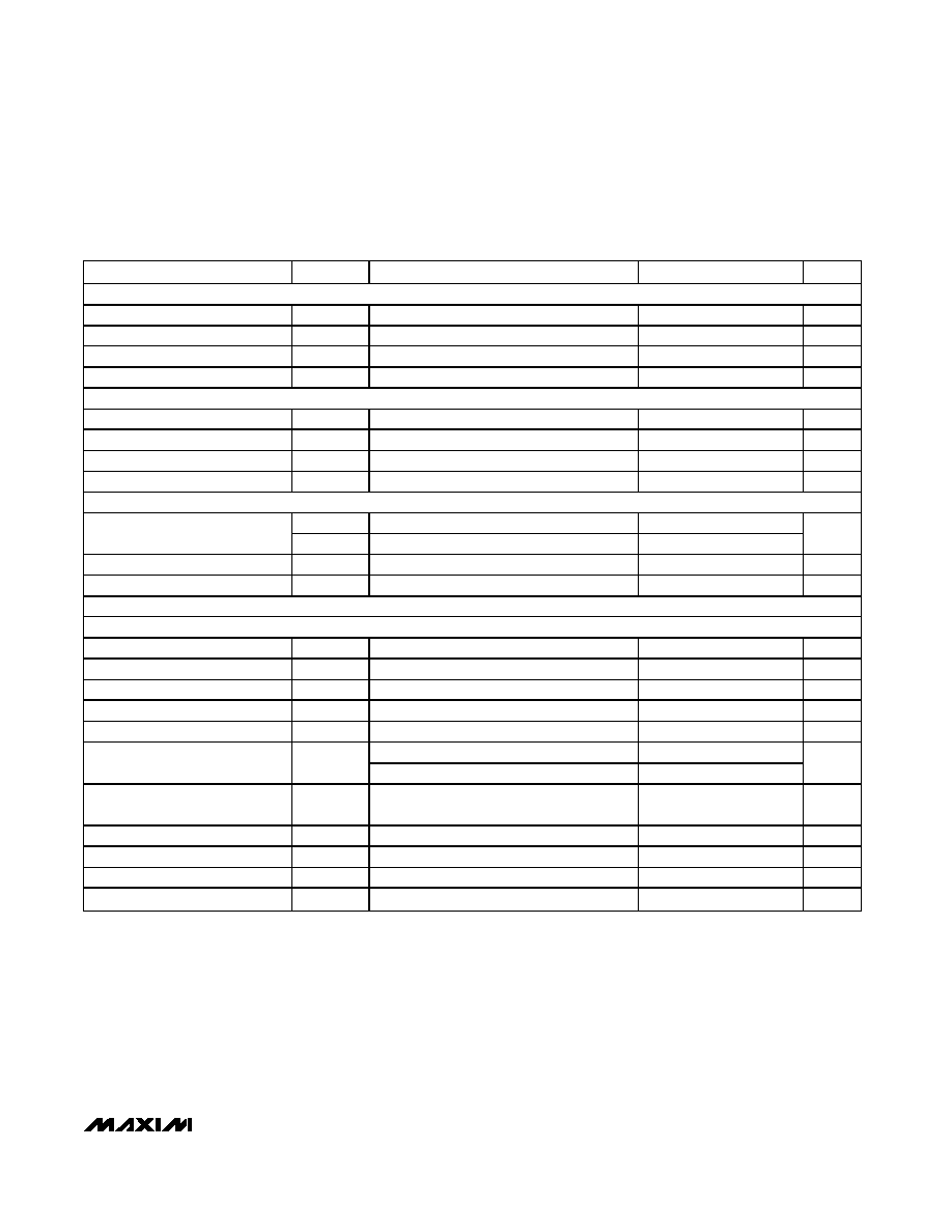
PARAMETER
SYM B O L
CONDITIONS
MIN
TYP
MAX
UNITS
Supply Voltage
V
CC
3.0
4.5
V
TRM Output Voltage
V
TRM
3.0
3.6
V
Logic Supply Voltage
V
L
1.65
3.60
V
V
L
Supply Current
I
VL
I
2
C interface in steady state
5
µA
V
CC
Operating Supply Current
I
CC
USB normal mode, C
L
= 50pF, device
switching at full speed
10
mA
vbus_drv = 1, I
VBUS
= 0
1.4
2
V
CC
Supply Current During Full-
Speed Idle
vbus_drv = 0, D+ = high, D- = low
0.5
0.8
mA
V
CC
Shutdown Supply Current
I
CC(SHDN)
3.5
10
µA
V
CC
Interrupt Shutdown Supply
Current
I
CC(ISHDN)
ID_IN floating or high
20
30
µA
V
CC
Suspend Supply Current
USB suspend mode, ID_IN floating or high
170
500
µA
LOGIC I/O
RC V , D AT_V P , S E 0_V M , INT,
OE/INT, V P , V M Outp ut H i g h
V ol tag e
V
OH
I
OUT
= 1mA (sourcing)
V
L
- 0.4
V
RCV, DAT_VP, SE0_VM, INT,
OE/INT, VP, VM Output Low
Voltage
V
OL
I
OUT
= 1mA (sinking)
0.4
V
OE/INT, SPD, SUS, RESET,
DAT_VP, SE0_VM Input High
Voltage
V
IH
2/3 x V
L
V

MAX3301E
USB On-the-Go Transceiver and Charge Pump
_______________________________________________________________________________________
3
DC ELECTRICAL CHARACTERISTICS (continued)
(V
CC
= +3V to +4.5V, V
L
= +1.65V to +3.6V, C
FLYING
= 100nF, C
VBUS
= 1µF, ESR
CVBUS
= 0.1
(max), T
A
= T
MIN
to T
MAX
, unless
otherwise noted. Typical values are at V
CC
= +3.7V, V
L
= +2.5V, T
A
= +25°C.) (Note 2)
PARAMETER
SYM B O L
CONDITIONS
MIN
TYP
MAX
UNITS
OE/INT, SPD, SUS, RESET
DAT_VP, SE0_VM Input Low
Voltage
V
IL
0.4
V
ADD Input High Voltage
V
IHA
2/3 x V
L
V
ADD Input Low Voltage
V
ILA
1/3 x V
L
V
Input Leakage Current
±1
µA
TRANSCEIVER SPECIFICATIONS
Differential Receiver Input
Sensitivity
|V
D+
- V
D-
|
0.2
V
Differential Receiver Common-
Mode Voltage
0.8
2.5
V
Single-Ended Receiver Input Low
Voltage
V
ILD
D+, D-
0.8
V
Single-Ended Receiver Input
High Voltage
V
IHD
D+, D-
2.0
V
S i ng l e- E nd ed Recei ver H yster esi s
0.2
V
S i ng l e- E nd ed Outp ut Low V ol tag e
V
OLD
D+, D-, R
L
= 1.5k
from D+ or D- to 3.6V
0.3
V
S i ng l e- E nd ed Outp ut H i g h V ol tag e
V
OHD
D+, D-, R
L
= 15k
from D+ or D- to GND
2.8
3.6
V
Off-State Leakage Current
D+, D-
±1
µA
Low steady-state drive
2
13
Driver Output Impedance
D+, D-, not
including R
EXT
High steady-state drive
2
13
ESD PROTECTION (V
BUS
, ID_IN, D+, D-)
Human Body Model
±15
kV
IEC 61000-4-2 Air-Gap Discharge
±10
kV
IEC 61000-4-2 Contact Discharge
±6
kV
THERMAL SHUTDOWN
Thermal Shutdown Low-to-High
+160
o
C
Thermal Shutdown High-to-Low
+150
o
C
CHARGE-PUMP SPECIFICATIONS (vbus_drv = 1)
V
BUS
Output Voltage
V
BUS
3V < V
C C
< 4.5V, C
V BUS
= 10µF, I
V BUS
= 8m A
4.80
5.25
V
V
BUS
Output Current
I
VBUS
8
mA
V
BUS
Output Ripple
I
VBUS
= 8mA, C
VBUS
= 10µF
100
mV

MAX3301E
USB On-the-Go Transceiver and Charge Pump
4
_______________________________________________________________________________________
DC ELECTRICAL CHARACTERISTICS (continued)
(V
CC
= +3V to +4.5V, V
L
= +1.65V to +3.6V, C
FLYING
= 100nF, C
VBUS
= 1µF, ESR
CVBUS
= 0.1
(max), T
A
= T
MIN
to T
MAX
, unless
otherwise noted. Typical values are at V
CC
= +3.7V, V
L
= +2.5V, T
A
= +25°C.) (Note 2)
PARAMETER
SYM B O L
CONDITIONS
MIN
TYP
MAX
UNITS
Switching Frequency
f
SW
390
kHz
V
BUS
Leakage Voltage
vbus_drv = 0
0.2
V
V
BUS
Rise Time
C
VBUS
= 10µF, I
VBUS
= 8mA, measured
from 0 to +4.4V
100
ms
V
BUS
Pulldown Resistance
vb us_d ischrg = 1, vb us_d r v = 0, vb us_chr g = 0
3.8
5
6.5
k
V
BUS
Pullup Resistance
vb us_chr g = 1, vb us_d r v = 0, vbus_di schr g = 0
650
930
1250
V
BUS
Input Impedance
Z
INVBUS
vb us_d ischrg = 0, vb us_d r v = 0, vb us_chr g = 0
40
70
100
k
COMPARATOR SPECIFICATIONS
V
B U S
V al i d C om p ar ator Thr eshol d
V
TH-VBUS
4.4
4.6
4.8
V
V
B U S
V al i d C om p ar ator H yster esi s
V
HYS-VBUS
50
mV
Session-Valid Comparator
Threshold
V
TH-
SESS_VLD
0.8
1.4
2.0
V
Session-End Comparator
Threshold
V
TH-
SESS_END
0.2
0.5
0.8
V
dp_hi Comparator Threshold
0.8
1.3
2.0
V
dm_hi Comparator Threshold
0.8
1.3
2.0
V
cr_int Pulse Width
750
ns
cr_int Comparator Threshold
0.4
0.5
0.6
V
ID_IN SPECIFICATIONS
ID_IN Input Voltage for Car Kit
0.2 x
V
CC
0.8 x
V
CC
V
ID_IN Input Voltage for A Device
0.1 x
V
CC
V
ID_IN Input Voltage for B Device
0.9 x
V
CC
V
ID_IN Input Impedance
Z
ID_IN
70
100
130
k
ID_IN Input Leakage Current
ID_IN = V
CC
-1
+1
µA
ID_IN Pulldown Resistance
id_pulldown = 1
150
300
TERMINATING RESISTOR SPECIFICATIONS (D+, D-)
D+ Pulldown Resistor
dp_pulldown = 1
14.25
15
15.75
k
D- Pulldown Resistor
dm_pulldown = 1
14.25
15
15.75
k
D+ Pullup Resistor
dp_pullup = 1
1.425
1.5
1.575
k
D- Pullup Resistor
dm_pullup = 1
1.425
1.5
1.575
k
MAX3301E
USB On-the-Go Transceiver and Charge Pump
_______________________________________________________________________________________
5
TIMING CHARACTERISTICS
(V
CC
= +3V to +4.5V, V
L
= +1.65V to +3.6V, C
FLYING
= 100nF, C
VBUS
= 1µF, ESR
CVBUS
= 0.1
(max), T
A
= T
MIN
to T
MAX
, unless
otherwise noted. Typical values are at V
CC
= +3.7V, V
L
= +2.5V, T
A
= +25°C.) (Note 2)
PARAMETER
SYM B O L
CONDITIONS
MIN
TYP
MAX
UNITS
TRANSMITTER CHARACTERISTICS (FULL-SPEED MODE)
D+, D- Rise Time
t
R
Figures 2 and 5
4
20
ns
D+, D- Fall Time
t
F
Figures 2 and 5
4
20
ns
Rise-/Fall-Time Matching
Figures 2 and 5 (Note 3)
90
110
%
Output-Signal Crossover Voltage
V
CRS_F
Figures 2, 6, and 7 (Note 3)
1.3
2.0
V
TRANSCEIVER CHARACTERISTICS (LOW-SPEED MODE)
D+, D- Rise Time
t
R
Figures 2 and 5
75
300
ns
D+, D- Fall Time
t
F
Figures 2 and 5
75
300
ns
Rise-/Fall-Time Matching
Figures 2 and 5
80
125
%
Output-Signal Crossover Voltage
V
CRS_L
Figures 2, 6, and 7
1.3
2.0
V
TRANSMITTER TIMING (FULL-SPEED MODE)
t
PLH
Low-to-high, Figures 2 and 6
25
Driver Propagation Delay
(DAT_VP, SE0_VM to D+, D-)
t
PHL
High-to-low, Figures 2 and 6
25
ns
Driver Disable Delay
t
PDZ
Figures 1 and 8
25
ns
Driver Enable Delay
t
PZD
Figures 2 and 8
25
ns
TRANSMITTER TIMING (LOW-SPEED MODE) (Low-speed delay timing is dominated by the slow rise and fall times.)
SPEED-INDEPENDENT TIMING CHARACTERISTICS
Receiver Disable Delay
t
PVZ
Figure 4
30
ns
Receiver Enable Delay
t
PZV
Figure 4
30
ns
D+ Pullup Assertion Time
During HNP
3
µs
RCV Rise Time
t
R
Figures 3 and 5, C
L
= 15pF
4
ns
RCV Fall Time
t
F
Figures 3 and 5, C
L
= 15pF
4
ns
Figures 3 and 10, |D+ - D-| to DAT_VP
30
Differential-Receiver Propagation
Delay
t
PHL
, t
PLH
Figures 3 and 9, |D+ - D-| to RCV
30
ns
Single-Ended-Receiver
Propagation Delay
t
PHL
, t
PLH
Figures 3 and 9, D+, D- to DAT_VP,
SE0_VM
30
ns
Interrupt Propagation Delay
100
µs
V
BUS_CHRG
Propagation Delay
Dominated by the V
BUS
rise time
0.2
µs
Time to Exit Shutdown
1
µs
Shutdown Delay
10
µs