General Description
The MAX3250 is a 3.0V to 5.5V powered, ±50V isolated
EIA/TIA-232 and V.28/V.24 communications interface
with high data-rate capabilities. The MAX3250 is a dual
die part that operates with up to ±50V difference
between the RS-232 side and the logic side (ISOCOM
to GND). This makes the device ideal for operation in
noisy conditions with high common-mode voltages.
This feature prevents damage to the device if RS-232
lines are inadvertently short-circuited to a +24V or ±48V
power bus.
The MAX3250 is powered by a single 3V to 5.5V supply
on the logic side. Power is transferred from the logic
side to the isolated side by ±100V external capacitors.
The MAX3250 has two receivers (Rx) and two drivers
(Tx) and is guaranteed to run at data rates of 250kbps
while maintaining RS-232 output levels. The trans-
ceivers have a proprietary low-dropout transmitter out-
put stage, delivering true RS-232 performance from a
3V to 5.5V supply with a dual charge pump. The device
features a FAULT open-drain output to signal an exces-
sive isolated-side voltage condition on any of the RS-
232 inputs. This output can drive an alarm LED or can
be monitored by the processor to prevent operation
under these conditions. The receiver outputs are high
impedance in shutdown, allowing multiple interfaces
(IrDA, RS-232, RS-485) to be connected to the same
UART.
The MAX3250 is available in a space-saving 28-pin
SSOP package.
Applications
Industrial Control
Programmable Logic Controller
Point-of-Sale Equipment
PC-to-Router Connections
Diagnostic Ports
Telecom Equipment
Features
o ±50V Isolation
o 20µA Supply Current in Shutdown
o 250kbps Guaranteed Data Rate
o FAULT Output
o High-Impedance Transmitter and Receiver
Outputs in Shutdown
o Space-Saving SSOP Package
o Inductorless/Transformerless Design Simplifies
EMI Compliance
o Low-Cost Replacement for Opto-Isolated
Transceivers
o Meets EIA/TIA-232 Specifications Down to 3.0V
MAX3250
±50V Isolated, 3.0V to 5.5V,
250kbps, 2 Tx/2 Rx, RS-232 Transceiver
________________________________________________________________ Maxim Integrated Products
1
Ordering Information
19-2443; Rev 1; 2/03
For pricing, delivery, and ordering information, please contact Maxim/Dallas Direct! at
1-888-629-4642, or visit Maxim's website at www.maxim-ic.com.
Typical Operating Circuit appears at end of data sheet.
PART
TEMP RANGE
PIN-PACKAGE
MAX3250CAI
0
°C to +70°C
28 SSOP
MAX3250EAI
-40
°C to +85°C
28 SSOP
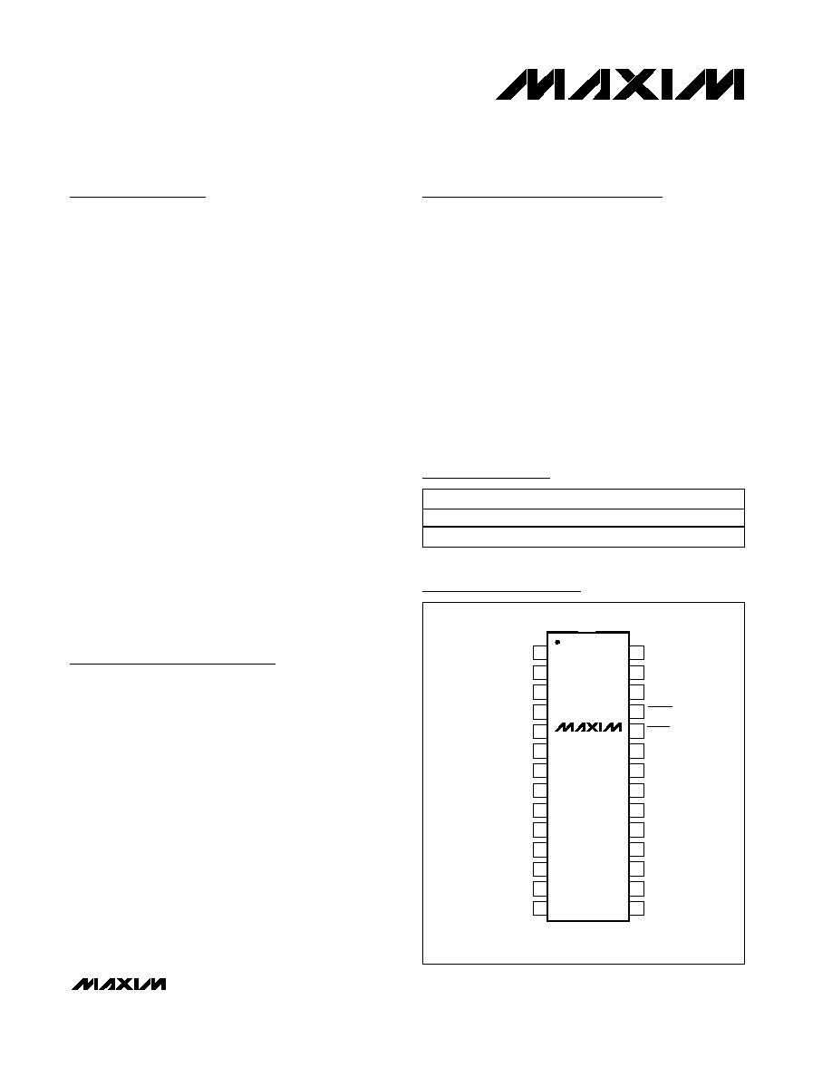
28
27
26
25
24
23
22
21
20
19
18
17
16
15
1
2
3
4
5
6
7
8
9
10
11
12
13
14
V
CC
C2-
GND
FAULT
SHDN
N.C.
ISOCOM
N.C.
C2+
ISOV
CC
R1IN
R2IN
T1OUT
T2OUT
V-
C4-
C4+
C3-
V+
C3+
C1+
N.C.
N.C.
T2IN
T1IN
R2OUT
R1OUT
C1-
SSOP
TOP VIEW
MAX3250
Pin Configuration
MAX3250
±50V Isolated, 3.0V to 5.5V,
250kbps, 2 TX/2 RX, RS-232 Transceiver
2
_______________________________________________________________________________________
ABSOLUTE MAXIMUM RATINGS
Stresses beyond those listed under "Absolute Maximum Ratings" may cause permanent damage to the device. These are stress ratings only, and functional
operation of the device at these or any other conditions beyond those indicated in the operational sections of the specifications is not implied. Exposure to
absolute maximum rating conditions for extended periods may affect device reliability.
All Voltages Referenced to GND, Unless Otherwise Noted.
V
CC
...........................................................................-0.3V to +6V
ISOCOM...............................................................................±80V
ISOV
CC
to ISOCOM..................................................-0.3V to +6V
V+ to ISOCOM (Note 1)............................................-0.3V to +7V
V- to ISOCOM (Note 1)............................................+0.3V to -7V
V+ + |V-| (Note 1) ...................................................................13V
Input Voltages
T_IN, SHDN ...........................................................-0.3V to +6V
R_IN to ISOCOM...............................................................±25V
Output Voltages
T_OUT to ISOCOM ........................................................±13.2V
R_OUT .....................................................-0.3V to (V
CC
+ 0.3V)
FAULT....................................................................-0.3V to +6V
C1-, C2- ......................................................-0.3V to (V
CC
+ 0.3V)
C1+, C2+, C3+, C3-, C4+, C4-
to ISOCOM ......................................-0.3V to (ISOV
CC
+ 0.3V)
T_OUT Current ..............30mA (continuous), 50mA (peak, 10µs)
R_IN Current..................30mA (continuous), 50mA (peak, 10µs)
ISOCOM Current ...........30mA (continuous), 50mA (peak, 10µs)
Short-Circuit Duration T_OUT to ISOCOM .................Continuous
Continuous Power Dissipation (T
A
= +70°C)
28-Pin SSOP (derate 9.5mW/°C above +70°C) ...........762mW
Operating Temperature Ranges
MAX3250CAI .....................................................0°C to +70°C
MAX3250EAI...................................................-40°C to +85°C
Storage Temperature Range .............................-65°C to +150°C
Lead Temperature (soldering, 10s) .................................+300°C
ELECTRICAL CHARACTERISTICS
(V
CC
= 3.0V to 5.5V, see Typical Operating Circuit and Table 1 for capacitor values, ISOCOM = GND, T
A
= T
MIN
to T
MAX
, unless oth-
erwise noted. Typical values are at V
CC
= 3.3V and T
A
= +25°C.) (Note 2)
PARAMETER
CONDITIONS
MIN
TYP
MAX
UNITS
DC CHARACTERISTICS
Supply Current
SHDN = V
CC
, no load
15
35
mA
SHDN = GND, V
ISOCOM
= GND
20
45
Supply Current Shutdown
SHDN = GND, V
ISOCOM
=
±50V
±350
µA
Maximum Ground Differential
|V
GND
- V
ISOCOM
|
50
V
Isolation Resistance
Between GND and ISOCOM
60
k
LOGIC INPUTS
Input Logic Low
T_IN, SHDN
0.8
V
V
CC
= 3.3V
2.0
Input Logic High
T_IN, SHDN
V
CC
= 5.0V
2.4
V
Transmitter Input Hysteresis
0.5
V
Input Leakage Current
T_IN, SHDN
-1
±0.01
+1
µA
RECEIVER OUTPUTS
Output Leakage Current
SHDN = GND
-10
±0.05
+10
µA
Output Voltage Low
I
OUT
= 1.6mA
0.4
V
Output Voltage High
I
OUT
= -1.0mA
V
CC
- 0.6 V
CC
- 0.1
V
FAULT OUTPUT
Output Voltage Low
(Open Drain)
I
OUT
= 5mA
0.4
V
Output Leakage Current
FAULT not asserted
1
µA
FAULT Trip Level
|V
GND
- V
ISOCOM
|
55
V
Note 1: V+ and V- can have a maximum magnitude of 7V, but their absolute difference cannot exceed 13V.
MAX3250
±50V Isolated, 3.0V to 5.5V,
250kbps, 2 TX/2 RX, RS-232 Transceiver
_______________________________________________________________________________________
3
ELECTRICAL CHARACTERISTICS (continued)
(V
CC
= 3.0V to 5.5V, see Typical Operating Circuit and Table 1 for capacitor values, ISOCOM = GND, T
A
= T
MIN
to T
MAX
, unless oth-
erwise noted. Typical values are at V
CC
= 3.3V and T
A
= +25°C.) (Note 2)
PARAMETER
CONDITIONS
MIN
TYP
MAX
UNITS
RECEIVER INPUTS (relative to ISOCOM)
Input Voltage Range
-25
+25
V
V
CC
= 3.3V
1.2
0.6
Input Threshold Low
T
A
= +25°C
V
CC
= 5.0V
1.3
0.8
V
V
CC
= 3.3V
2.4
1.6
Input Threshold High
T
A
= +25°C
V
CC
= 5.0V
2.4
1.7
V
Input Hysteresis
0.5
V
Input Resistance
T
A
= +25°C
3
5
7
k
TRANSMITTER OUTPUTS (relative to ISOCOM)
Output Voltage Swing
All transmitter outputs loaded with 3k
to ISOCOM
±5.0
±5.4
V
Output Resistance
ISOV
CC
= V+ = V- = 0V, T_OUT =
±2V
300
10M
Output Short-Circuit Current
-60
+60
mA
Output Leakage Current
V
CC
= 0 or 3V to 5.5V, T_OUT =
±12V, SHDN = GND
-25
+25
µA
TIMING CHARACTERISTICS
(V
CC
= 3.0V to 5.5V, see Typical Operating Circuit and Table 1 for capacitor values, ISOCOM = GND, T
A
= T
MIN
to T
MAX
, unless oth-
erwise noted. Typical values are at V
CC
= 3.3V and T
A
= +25°C.)
PARAMETER
CONDITIONS
MIN
TYP
MAX
UNITS
Maximum Data Rate
R
L
= 3k
, C
L
= 1000pF to ISOCOM, one transmitter
250
kbps
Receiver Propagation Delay
R_IN to R_OUT, C
L
= 150pF to GND
0.4
µs
Receiver Skew
|t
PHL
- t
PLH
|
100
ns
Transmitter Skew
|t
PHL
- t
PLH
| (Note 3)
120
ns
C
L
= 150pF to 1000pF
to ISOCOM
6
30
Transition-Region Slew Rate
V
CC
= 3.3V, T
A
= +25°C,
R
L
= 3k
to 7k to ISOCOM,
measured from +3V to -3V or
-3V to +3V
C
L
= 150pF to 2500pF
to ISOCOM
4
30
V/µs
FAULT Propagation Delay
0.3
µs
Time to Shutdown
0.5
µs
V
ISOCOM
= GND
300
Time to Exit Shutdown
V
ISOCOM
=
±50V
350
µs
Note 2: All currents into the device are positive; all currents out of the device are negative. All voltages are referenced to device
ground, unless otherwise noted.
Note 3: Transmitter skew is measured at the transmitter zero crosspoints.

MAX3250
±50V Isolated, 3.0V to 5.5V,
250kbps, 2 TX/2 RX, RS-232 Transceiver
4
_______________________________________________________________________________________
Typical Operating Characteristics
(V
CC
= 3.3V, 250kbps data rate, see Typical Operating Circuit and Table 1 for capacitor values, all transmitters loaded with 3k
and
C
L
to ISOCOM, T
A
= +25°C, unless otherwise noted.)
MAX3250 toc05
TEMPERATURE (
°C)
SUPPLY CURRENT (
µ
A)
60
35
10
-15
-200
-100
0
100
200
300
400
-300
-40
85
SHUTDOWN CURRENT
vs. TEMPERATURE
ISOCOM = -50V
ISOCOM = 0V
ISOCOM = +50V
TIME TO EXIT SHUTDOWN
V
ISOCOM
= 0V
TOUT
5V/div
MAX3250 toc04
100
µs/div
SHDN
5V/div
MAX3250 toc03
LOAD CAPACITANCE (pF)
SUPPLY CURRENT (mA)
4000
3000
2000
1000
10
20
30
40
50
60
70
80
90
0
0
5000
T1 TRANSMITTING AT 250kbps
T2 TRANSMITTING AT 20kbps
OPERATING SUPPLY CURRENT
vs. LOAD CAPACITANCE
250kbps
120kbps
20kbps
MAX3250 toc02
LOAD CAPACITANCE (pF)
SLEW RATE (V/
µ
s)
4000
3000
2000
1000
5
10
15
20
25
30
0
0
5000
SLEW RATE
vs. LOAD CAPACITANCE
-SLEW
+SLEW
FOR DATA RATES UP TO 250kbps
MAX3250 toc01
LOAD CAPACITANCE (pF)
TRANSMITTER OUTPUT VOLTAGE (V)
4000
3000
2000
1000
-4
-2
0
2
4
6
8
-6
0
5000
TRANSMITTER OUTPUT VOLTAGE
vs. LOAD CAPACITANCE
V
OUT+
V
OUT-
T1 TRANSMITTING AT 250kbps
T2 TRANSMITTING AT 20kbps
COMMON-MODE FAULT RESPONSE
ISOCOM
50V/div
MAX3250 toc07
FAULT
5V/div
4ms/div
PEAK GROUND OFFSET VOLTAGE
vs. FREQUENCY
MAX3250 toc06
FREQUENCY (Hz)
PEAK GROUND OFFSET (
±
V)
300
100
200
400
500
10
20
30
40
50
60
0
0
600
V
CC
= 3.3V
V
CC
= 5V

MAX3250
±50V Isolated, 3.0V to 5.5V,
250kbps, 2 TX/2 RX, RS-232 Transceiver
_______________________________________________________________________________________
5
Pin Description
PIN
NAME
FUNCTION
1
C1-
Negative Terminal of the Power Isolation Capacitor. Connect a 100V capacitor from C1- to C1+.
See Table 1 for values.
2
R1OUT
TTL/CMOS Receiver Output
3
R2OUT
TTL/CMOS Receiver Output
4
T1IN
TTL/CMOS Transmitter Input
5
T2IN
TTL/CMOS Transmitter Input
6, 22, 23
N.C.
No Connection. Not internally connected.
7
N.C.
No Connection. Leave unconnected or connect to ISOCOM.
8
C1+
Positive Terminal of the Power Isolation Capacitor. Connect a 100V capacitor from C1+ to C1-.
See Table 1 for values.
9
C3+
Positive Terminal of the Voltage-Doubler Charge-Pump Capacitor. Connect a 0.1µF capacitor from
C3+ to C3-.
10
V+
+5.5V Generated by the Charge Pump, Referenced to ISOCOM. Bypass V+ to ISOCOM with a
0.47µF capacitor.
11
C3-
Negative Terminal of the Voltage-Doubler Charge-Pump Capacitor. Connect a 0.1µF capacitor from
C3- to C3+.
12
C4+
Positive Terminal of the Inverting Charge-Pump Capacitor. Connect a 0.47µF capacitor from
C4+ to C4-.
13
C4-
Negative Terminal of the Inverting Charge-Pump Capacitor. Connect a 0.47µF capacitor from
C4- to C4+.
14
V-
-5.5V Generated by the Charge Pump, Referenced to ISOCOM. Bypass V- to ISOCOM with a 0.47µF
capacitor.
15
ISOCOM
Isolated Ground
16
T2OUT
RS-232 Transmitter Output
17
T1OUT
RS-232 Transmitter Output
18
R2IN
RS-232 Receiver Input
19
R1IN
RS-232 Receiver Input
20
ISOV
CC
Internally Generated Isolated Power-Supply Voltage, Referenced to ISOCOM. Bypass ISOV
CC
to
ISOCOM with a 1µF capacitor.
21
C2+
Positive Terminal of the Power Isolation Capacitor. Connect a 100V capacitor from C2+ to C2-.
See Table 1 for values.
24
SHDN
Shutdown Control. Drive SHDN low to enter low-power shutdown mode. Drive SHDN high or connect
to V
CC
for normal operation.
25
FAULT
Overvoltage Indicator. Active low, open drain.
26
GND
Ground
27
C2-
Negative Terminal of the Power Isolation Capacitor. Connect a 100V capacitor from C2- to C2+.
See Table 1 for values.
28
V
CC
3.0V to 5.5V Supply Voltage. Bypass V
CC
to GND with a 1µF capacitor.